
 Open Access Article
 This Open Access Article is licensed under a Creative Commons Attribution-Non Commercial 3.0 Unported Licence
A type-II blue phosphorus/MoSe2 van der Waals heterostructure: improved electronic and optical properties via vertical electric field†
Huabing
Shu

School of Science, Jiangsu University of Science and Technology, Zhenjiang 212001, China. E-mail: shuhuabing@just.edu.cn
First published on 25th July 2020
Abstract
Building novel van der Waals (vdW) heterostructures is of great interest and is important to improve the performance of individual two-dimensional materials. Using first-principles calculations, we demonstrate that the constructed blue phosphorus/MoSe2 (P2/MoSe2) vdW heterostructure has a unique type-II band alignment and a suitable bandgap (about 1.63 eV) for optoelectronic applications. Its electronic and optical properties depend strongly on the applied vertical electric field. The quasi-particle bandgap of the P2/MoSe2 can be linearly modulated by about 1.11 eV under the applied electric field and the type-II band alignment persists in a broad range. Meanwhile, the negative electric field induces a significant red-shift of the optical absorption edge of P2/MoSe2, greatly enhancing its absorption for the visible and near-infrared lights, which is desirable for optoelectronic applications. More importantly, the observed interlayer excitons with large binding energy (more than 600 meV) can be preserved under the applied electric field, being very much beneficial for the real separation of photoexcited carriers. These results indicate that the P2/MoSe2 vdW heterostructure can become a good candidate for optoelectronic devices.
1 Introduction
In recent years, the precise transfer of the produced two-dimensional (2D) materials has led to an emerging new class of materials, van der Waals (vdW) heterostructures.1–8 vdW heterostructures, formed by vertically stacking two dissimilar 2D materials, can exhibit more desirable properties than their components due to interlayer coupling. For example, the interlayer coupling induced by vdW interactions can cause an ultrafast separation of photoexcited carriers9–11 and long lifetimes of indirect excitons in the vdW heterostructure.12,13 Such novel properties in vdW heterostructures can be utilized to explore their applications for photovoltaics and optoelectronics. Previously, an efficient flexible photovoltaic device based on graphene/MoS2 was reported, achieving an external quantum efficiency of above 30%.14 A p–n diode based on black phosphorene/MoS2 obtains broad-band photodetection and sunlight harvesting.15 The vdW heterostructures for other versatile applications also have been reported, including electrocatalysts,16,17 Li+/Na+ ion batteries,18,19 and supercapacitors.20,21 In addition, the external electric field has also been considered as an effective way to further optimize the properties of vdW heterostructures. The electric-field tunable semiconductor-to-metal transition is observed in black phosphorene/MoS2,22 MoS2/MX2 (M: Mo, W, and Cr; X = Se, and S),23 and black phosphorene (MoSSe)/blue phosphorene heterostructures,24,25 suggesting a new application of these systems in semiconductor devices. More importantly, the external electric field can significantly manipulate the optical properties of the vdW heterostructure by changing the band alignment and interlayer coupling.26,27 For example, in the WSe2/graphene vdW heterostructure, the external electric field enhances photoluminescence (PL) intensity of excitons by more than 40 times and induces a maximum blue-shift of 50 meV of exciton peaks.28Among 2D materials, the hexagonal MoSe2 monolayer has desirable properties, such as a direct bandgap of 1.60 eV,29,30 optical absorbance of 5–10% for the incident sunlight, and a photo flux of 4.6 mA cm−2.31 Monolayer MoSe2-based field effect transistors can also obtain an on/off current ratio as high as 106 and an intrinsic carrier mobility of up to 500 cm2 V−1 s−1 at 100 K.32 In 2016 the blue phosphorus (P2) monolayer with in-plane hexagonal structure was firstly synthesized on Au(111) by a molecular beam epitaxial growth approach.33 Furthermore, theoretical studies have demonstrated that it has intriguing structural and electronic properties, such as its stability at room temperature,34,35 moderate bandgap of approximately 2.0 eV,35,36 and room-temperature carrier mobility of over 103 cm2 V−1 s−1.37 These good properties in MoSe2 and P2 monolayers can draw enormous interest, suggesting great potential in optoelectronic devices. Besides, the MoSe2 and P2 monolayers with similar hexagonal structure35,38 have distinct differences in constituents and chemical bonding, which may form a large potential difference and band offsets between the two layers. Meanwhile, it suggests that the hybrid band structure, band alignment at the heterointerface, and even interlayer coupling in the vdW heterostructure based on MoSe2 and P2 monolayers, can be manipulated by an external electric field. Previously, MoSe2-based vdW heterostructures, such as WS2/MoSe239,40 and WSe2/MoSe2,41 have been achieved by transfer methods. Therefore, the fabrication of a P2/MoSe2 vdW heterostructure is anticipated and their properties are of great interest.
In this work, we construct five P2/MoSe2 vdW heterostructures by stacking the P2 and MoSe2 monolayers. Using density-functional theory (DFT) connected with the G0W0 + Bethe–Salpeter equation (BSE) method, we investigated the P2/MoSe2 vdW heterostructure, focusing on the structure, electronic and optical properties, and the effect of vertical electric field. Our calculations show that its electronic band structure and optical response are very sensitive to the size and orientation of the applied electric field.
2 Computational method
The electronic and optical properties of the systems were attained via a three-step procedure. First, we used a plane-wave basis set and a norm-conserving pseudopotential42 to achieve the ground states, which was performed by the Quantum Espresso code.43 Electron exchange and correlation were treated by generalized gradient approximation (GGA) along with the Perder–Burke–Ernzerhof (PBE) functional.44 The 4s24p64d55s1 of Mo, 4s24p6 of Se, and 3s23p3 of P were used as valence electrons. The cutoff energy for wave function was set to be 70 Ry. To eliminate the interaction between spurious replicate images, a vacuum region of 20 Å along the c-axial direction was inserted for the systems. The Brillouin zone integrations adopted a k-point grid of 18 × 18 × 1. The weak interaction between two layers was considered via a vdW-DF approach.45,46 When structures were fully relaxed, the force applied on each atom and the total energy of the system were converged within the 0.01 eV Å−1 and 10−4 eV, respectively. To avoid the errors induced by the periodic boundary condition, dipole correction was considered in the systems. Furthermore, an external sawtooth potential along the c-axial direction was also used to simulate the effect of an applied electric field.47 The phonon dispersion relations of the systems were obtained by performing phonon calculations from density functional perturbation theory.48Then, the G0W0 approximation49 was used to obtain quasi-particle (QP) band structures. The convergence of quasi-particle bandgap with respect to the number of unoccupied bands, the size of dielectric matrix and the k-point grid was carefully checked and a convergence of 100 meV was assured in the systems. Finally, the coupled electron–hole excitation energies and exciton wave functions were obtained by solving the Bethe–Salpeter equation (BSE).50,51 The 1218 bands (unoccupied bands: 1200, and occupied bands: 18) and random phase approximation were involved to attain the converged dielectric function. A fine k-point grid (54 × 54 × 1), 38 bands (20 unoccupied bands), was utilized to obtain the converged optical spectra. The G0W0 and BSE calculations were performed via the YAMBO code.52
3 Results and discussion
3.1 Geometric structure and stability
Before investigating the P2/MoSe2 vdW heterostructure, it is necessary to understand the geometries and electronic properties of P2 and MoSe2 monolayers. Their optimized geometric structures are provided in Fig. S1 of the ESI,† in which the lattice constants are aP2 = bP2 = 3.322 Å for the P2 monolayer and aMoSe2 = bMoSe2 = 3.269 Å for the MoSe2 monolayer. The bond lengths of P–P and Mo–Se are 2.271 Å and 2.549 Å, respectively. The obtained structural parameters are in good accordance with previous studies.35,53,54 To examine the electronic properties of the P2 and MoSe2 monolayers, the quasi-particle band structures with many-body interaction included, are calculated by the single-shot G0W0 method and the results are exhibited in Fig. S2 (ESI†). It can be found that the P2 monolayer is an indirect semiconductor with a wide quasi-particle gap of 3.350 eV, while the MoSe2 monolayer has a direct bandgap of 2.300 eV at K-point. Interestingly, the gap of the MoSe2 monolayer is fixed at the visible-light region, suggesting its potential for visible-light-driven optoelectronics. The predicted quasi-particle bandgaps agree well with previous reports (3.530 eV for P2 monolayer; 2.260 eV for MoSe2 monolayer).54–56Due to small lattice mismatch (approximately 1.6%) between the P2 and MoSe2 monolayers, five P2/MoSe2 vdW heterostructures are constructed by the 1 × 1 primitive cells of the P2 and MoSe2 monolayers, as shown in Fig. 1. The lattice mismatch is calculated by 2(aP2 − aMoSe2)/(aP2 + aMoSe2). To verify the thermal stability of the five possible stacking configurations, the formation energies (Ef) are firstly calculated to assess them using the equation Ef = E1 − E2 − E3, where E1, E2, and E3 are the total energies of the P2/MoSe2, P2 monolayer, and MoSe2 monolayer, respectively. The estimated formation energies are all negative for these designed configurations (as seen in Table S1, ESI†), suggesting that the fabrications of P2/MoSe2 vdW heterostructures should be feasible from a thermodynamic point of view. Among these constructed vdW heterostructures, the AA-I stacking shows the most stable structure by the lowest formation energy of −0.212 eV per unit cell. We further verify the dynamical stability of these heterostructures by calculating their phonon spectra, which are shown in Fig. 2(b)–(f). The observed phonon spectra of AA-I and AB-III stacking structures have no negative frequencies, while the other three stacking configurations (AA-II, AB-I, and AB-II) have negligible imaginary frequencies around the Γ-point. The calculation results of phonon dispersion indicate that the AA-I and AB-III configurations have more dynamical stability than the other three configurations. In addition, as a comparison, the structural parameters of the five configurations are also listed in Table S1 (ESI†). There is little difference in the lattice constant, bond length, and interlayer distance for the five stacking configurations, which will result in similar band dispersion, as seen in Fig. S3 (ESI†). In the following sections, we only investigate the most stable AA-I configuration among five stacking configurations.
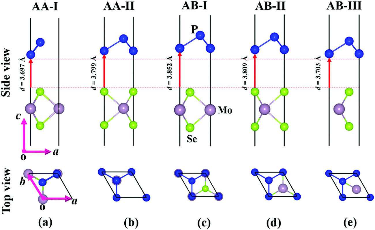 | ||
| Fig. 1 Optimized structures of P2/MoSe2 vdW heterostructures with different stacking configurations: (a) AA-I, (b) AA-II, (c) AB-I, (d) AB-II, and (e) AB-III. | ||
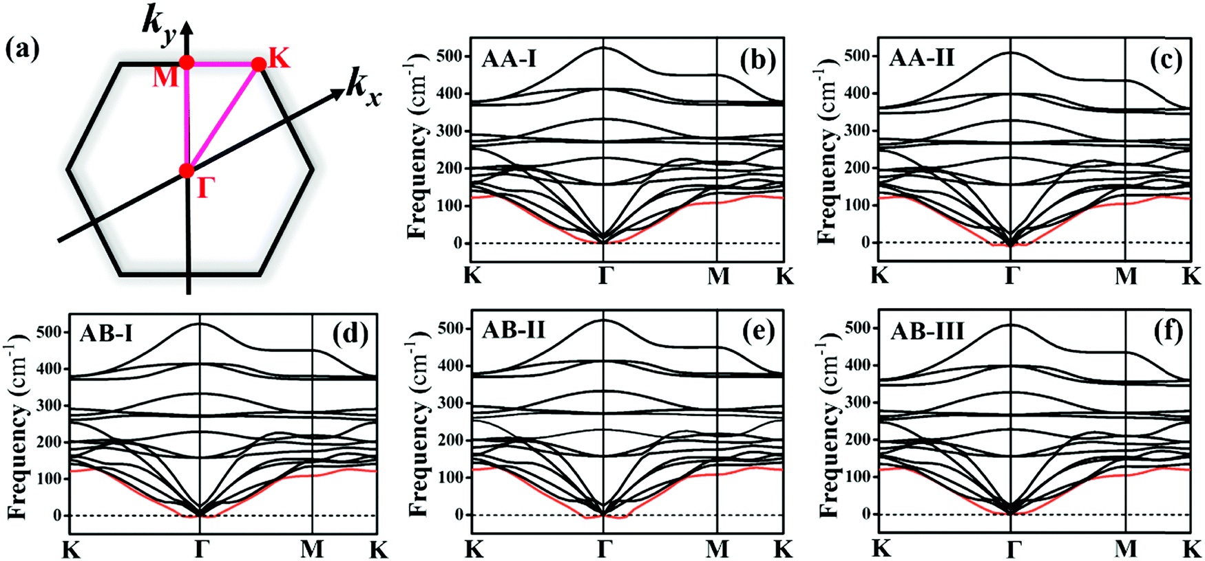 | ||
| Fig. 2 (a) High-symmetric path (K–Γ–M–K) of the first Brillouin zone of hexagonal lattice, K (1/3, 1/3, 0), Γ (0, 0, 0), and M (0, 1/2, 0). Phonon spectra of P2/MoSe2 vdW heterostructures with different stacking configurations: (b) AA-I, (c) AA-II, (d) AB-I, (e) AB-II, and (f) AB-III. | ||
3.2 Electronic and optical properties
Fig. 3(a) shows the quasi-particle band structure of the AA-I stacking P2/MoSe2 vdW heterostructure at the single-shot G0W0 level. Compared with the isolated P2 and MoSe2 monolayers, the P2/MoSe2 vdW heterostructure has a relatively narrow indirect gap of 1.630 eV due to the preserved band structures of the two monolayers. This phenomenon has also been observed in other semiconducting vdW heterostructures, such as WS2/MoS2, blue phosphorene/BSe, and blue phosphorus/Mg(OH)2.58–60 To understand the layer contributions to the highest occupied state (VBM) and the lowest unoccupied state (CBM) of the P2/MoSe2, the partial charge distributions of the CBM and VBM are calculated and the results are exhibited in Fig. 3(a) right. It is found the CBM and VBM of the P2/MoSe2 are contributed by the P2 and MoSe2 layers, respectively, suggesting it has a type-II characteristic of band alignment and good charge separation. To check the charge transfer between the P2 and MoSe2 layers, it is necessary to obtain the work functions (Φ) of the isolated P2 and MoSe2 monolayers. The Φ can be calculated by the definition: Φ = EVAC − EVBM, in which EVAC and EVBM are the vacuum potential and VBM energy, respectively.61 The obtained work functions are 6.96 eV for the P2 monolayer and 5.46 eV for the MoSe2 monolayer, respectively. Owing to a relatively large difference (1.50 eV) in the work functions between the P2 and MoSe2 monolayers, electrons can easily migrate from the MoSe2 layer into the P2 layer after forming the P2/MoSe2 vdW heterostructure. The work function of P2/MoSe2 is also estimated to be 4.95 eV, being less than those of the isolated monolayers due to the interlayer coupling. Also, the calculated two band edges of the heterostructure relative to the vacuum level are located at −3.32 eV (CBM) and −4.95 eV (VBM), which cannot wholly straddle water redox potentials (reduction potential: −4.44 eV; oxidation potential: −5.67 eV) at pH = 0. However, the P2/MoSe2 vdW heterostructure satisfies the reduction level in water splitting. Upon illuminating the P2/MoSe2, the photoexcited electrons collected in the P2 layer due to the type-II band alignment will drive the hydrogen reduction reaction generating hydrogen (2H+ + 2e− → H2), as shown in Fig. S4 (ESI†), suggesting it could be a potential hydrogen production material.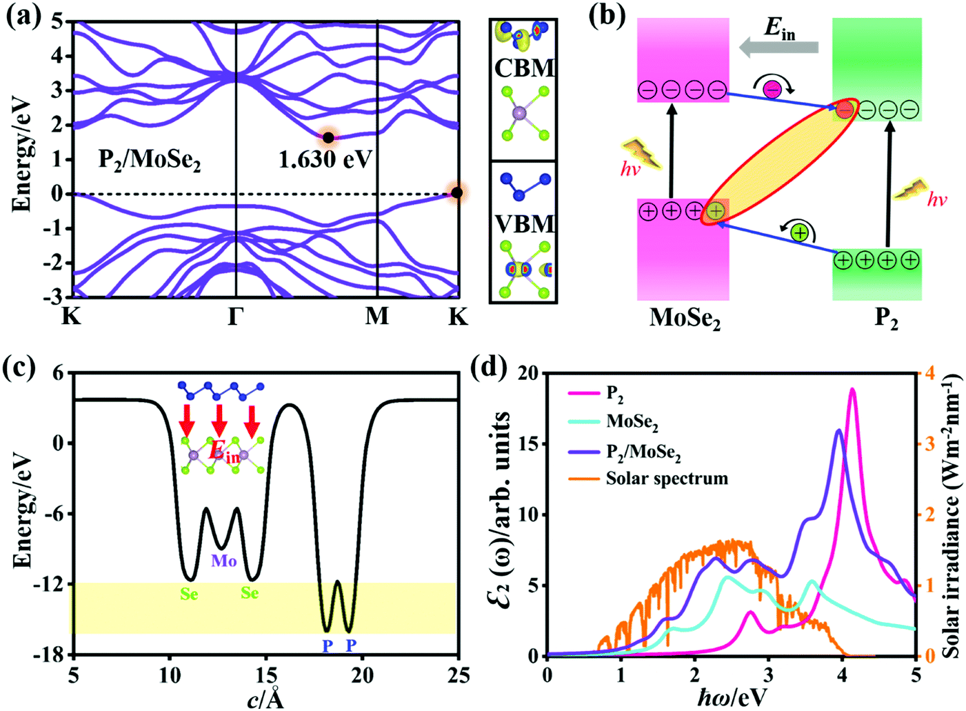 | ||
| Fig. 3 (a) Quasi-particle band structure and decomposed charge density (CBM and VBM) of the P2/MoSe2 vdW heterostructure (isosurface: 3.0 × 10⁻³ e Å−3). (b) Schematic diagram of the band alignment between the two layers in P2/MoSe2 and charge separation at the P2–MoSe2 interface. (c) Planar average electrostatic potential of the P2/MoSe2 along the c-axial direction. The direction of built-in electric field (Ein) is inset. (d) Optical absorption spectra of the P2 and MoSe2 monolayers, and P2/MoSe2 including the interaction between photoexcited electrons and holes, in comparison with the incident AM 1.5G solar irradiance.57 Polarized light along the a-axial direction and Lorentzian broadening (0.15 eV) are used in these spectra. | ||
Fig. 3(b) shows the charge separation at the P2–MoSe2 interface and the formation of indirect excitons when illuminating the P2/MoSe2 vdW heterostructure. The photoexcited electrons and holes are inclined to spontaneously separate into the opposite layers by the potential offsets. The formed indirect excitons will prolong the lifetime of photoexcited carriers, being very useful for optoelectronic devices. In fact, the indirect charge-transfer exciton has been observed experimentally in other vdW heterostructures (like MoS2/WS2, MoS2/MoSe2, and MoS2/WSe2) by time resolved measurements9,62 and photoluminescence quenching.58,63,64 In addition, the planar average electrostatic potential is also computed and presented in Fig. 3(c). The depth of potential of the MoSe2 layer is smaller than that of the P2 layer by about 4 eV, indicating that the built-in electric field (Ein) has been formed in the MoSe2–P2 interface. The direction of the Ein is pointed from the P2 layer to the MoSe2 layer (as seen in the inset of Fig. 3(c)), which will play an important role in further facilitating charge separation, i.e. the photoexcited electron (hole) is accelerated to flow from the MoSe2 (P2) layer to the P2 (MoSe2) layer under the Ein (as in Fig. 3(b)). As a result, the Ein can promote the separation of photoexcited electron–hole pairs in the P2/MoSe2 vdW heterostructure.
On the other hand, the excitonic behavior of the P2/MoSe2 vdW heterostructure should have a striking difference with those of the isolated P2 and MoSe2 monolayers owing to the existence of a potential gradient across the P2–MoSe2 interface. In order to obtain their exact optical properties, we solved the BSE equation based on the G0W0 calculations, which has fully included the many-body interactions (electron–electron and electron–hole interactions) in real systems. Fig. 3(d) shows the imaginary parts ε2(ω) of the dielectric functions of the P2 monolayer, MoSe2 monolayer, and the P2/MoSe2 heterostructure, i.e. the optical absorption spectra. It can be found that the P2/MoSe2 heterostructure has a wide absorption range from the near-infrared to the near-ultraviolet. The optical spectrum of the P2/MoSe2 is dominated by the MoSe2 layer in the energy of 0–2 eV, while the absorption ranging from 2 eV to 5 eV is contributed by both the MoSe2 and P2 layers. Compared with the isolated P2 and MoSe2 monolayers, the P2/MoSe2 vdW heterostructure has a marked enhancement of optical absorption in a broad light-harvesting range, spanning from 1.64 eV (visible light) to 4.15 eV (near-ultraviolet light). The enhanced optical absorption in the P2/MoSe2 vdW heterostructure should originate from the interlayer coupling and charge transfer between the two single layers as well as the overlap of the electronic states. In addition, for the incident AM 1.5G solar irradiance, the P2/MoSe2 vdW heterostructure can also absorb a considerable part, as shown in Fig. 3(d), which could be used in optoelectronic devices based on the solar irradiance.
3.3 Effects of vertical electric fields on electronic and optical properties
To explore the effect of electric field on the electronic properties of the P2/MoSe2 vdW heterostructure, an electric field (Eef) perpendicular to the stacking layers is applied on the heterostructure, ranging from −0.4 V Å−1 to 0.4 V Å−1 with the step of 0.1 V Å−1. The phonon spectrum of P2/MoSe2 at the electric field of 0.4 V Å−1 is also calculated to check its dynamical stability, as presented in Fig. S5 (ESI†). Only a small imaginary frequency of −1.8 cm−1 close to the Γ point is observed in the P2/MoSe2, suggesting it has dynamic stability under the observed electric field. The positive direction of vertical electric field is pointed from the MoSe2 layer to the P2 layer along the c-axial direction. Experimentally, a controlled vertical electric field can be realized by a double-gated configuration without changing the charge carrier concentration in the P2/MoSe2 vdW heterostructure, as shown in Fig. 4(a). Fig. 4(b) shows the various bandgaps under different electric-field strengths from the PBE and G0W0 methods. The G0W0 method can correct the band structure of the semiconductor at the PBE level to obtain a credible quasi-particle bandgap by shifting the conduction (valence) band up (down). It can be seen that the quasi-particle bandgap of the P2/MoSe2 heterostructure can be significantly tuned in a wide range from 0.94 eV (Eef = −0.4 V Å−1) to 2.05 eV (Eef = 0.4 V Å−1). Although the PBE method underestimates the bandgap of the semiconducting material, the trend of bandgap variation in the two methods is roughly the same in the observed electric field range, in which the bandgap linearly increases with Eef from −0.4 V Å−1 to 0.24 V Å−1 and shows little change from 0.24 V Å−1 to 0.4 V Å−1. To shed more light on the variable bandgap, the projected band structures of P2/MoSe2 under variable electric fields is calculated and presented in Fig. 5(a)–(e). It is found that the CBM (A point) belonging to the P2 layer is very sensitive to Eef, in which the A point is slowly elevated in the range of −0.4 to 0.2 V Å−1, leading to the increasing bandgap of the P2/MoSe2. In fact, the CBM has been shifted to the B point located at the MoSe2 layer at Eef = 0.24 V Å−1, shown in Fig. 5(f), suggesting that the type-II band alignment in the P2/MoSe2 heterostructure is converted to type-I at Eef = 0.24 V Å−1. When the Eef is larger than 0.24 V Å−1, the invariable bandgap of the P2/MoSe2 should be attributed to the insensitive B point to the applied electric field. Interestingly, for the P2/MoSe2 vdW heterostructure, the retained type-II heterointerface in a wide range from −0.4 to 0.24 V Å−1, together with broadly tunable bandgap, will endow it with potential applications in the optoeletronics and solar energy conversion.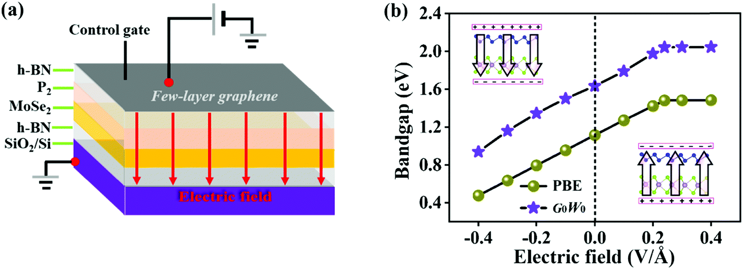 | ||
| Fig. 4 (a) Schematic of double-gated P2/MoSe2 device. (b)Evolution of bandgap as a function of the vertical electric field in the P2/MoSe2 vdW heterostructure. Two insets show the positive and negative directions of the vertical electric field, respectively. | ||
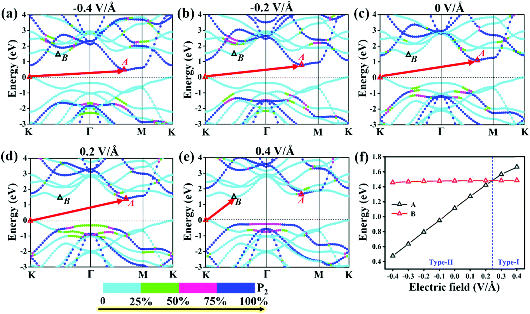 | ||
| Fig. 5 (a)–(e) Projected band structures of the P2/MoSe2 vdW heterostructure and (f) relative positions of “A” and “B” to the VBM at PBE level under a variable electric field. | ||
To obtain more physical insight into the P2/MoSe2 heterostructure, the planar-averaged electron density difference is also calculated along the c-axial direction under the Eef, as shown in Fig. 6. When applying an enhanced positive Eef, more electrons (Δq) flow from the P2 layer to the MoSe2 layer, which will generate an interlayer dipole moment P, causing the electric polarized field Eepf across the interlayer region of the P2/MoSe2. The direction of the Eepf points from the P2 layer to the MoSe2 layer, being opposite with the positive direction of the Eef. Such an Eepf across the P2–MoSe2 interface is beneficial to the separation of photoexcited carriers on the interface, shown in Fig. S6 (ESI†). On the contrary, more electrons tend to transfer from the MoSe2 layer to the P2 layer under an increased reverse Eef. Bader charge analysis further verifies that Δq = 1.15 × 10⁻²e, 4.9 × 10⁻³e, and −1.2 × 10⁻³e are transferred from the P2 layer to MoSe2 layer at Eef = 0.4 V Å−1, 0 V Å−1, and −0.4 V Å−1, respectively. Furthermore, the magnitude of electric polarized field (Eepf) can be estimated by Eepf = P/ε0·εr·S0·d. P is the size of the dipole moment and P = |Δq|·d, ε0 and εr are the permittivity of free space and relative dielectric constant (ε0 = 8.850 × 10⁻¹² F m−1, εr = 1.0), respectively, S0 is the interface area of the P2/MoSe2 (S0 = 9.380 × 10⁻²⁰ m2), and d is the interlayer equivalent distance (d = 3.697 × 10⁻¹⁰ m). The calculated Eepf under different Eef values can be found in Table S2 (ESI†). When Eef is strengthened to 0.40 V Å−1, the induced Eepf with opposite direction can be as large as 0.22 V Å−1, which is comparable to the applied vertical electric field. Thus, the vertical electric field may not only effectively tailor the carrier concentrations of the MoSe2 and P2 layers, but also change the interlayer coupling at the P2–MoSe2 heterointerface.
 | ||
| Fig. 6 Planar-averaged electron density difference across the P2/MoSe2 vdW heterostructure under various electric fields of −0.4 V Å−1, −0.2 V Å−1, 0 V Å−1, 0.2 V Å−1, and 0.4 V Å−1. The orange (blue) region corresponds the the MoSe2 (P2) layer. | ||
As mentioned before, there is a significant difference in the band structure of the P2/MoSe2 vdW heterostructure under different vertical electric fields. To further investigate the variation in the optical properties of the P2/MoSe2 at different electric field strengths, we calculated the ε2(ω) of the P2/MoSe2 at electric fields of −0.4 V Å−1, 0 V Å−1, and 0.4 V Å−1 and the results are plotted in Fig. 7, in which two polarized lights along the zigzag (a-axial) and armchair directions are adopted, respectively. From Fig. 7(a)–(c), strong isotropy is observed between ε2 (zigzag) and ε2 (armchair), suggesting that the isotropic nature of optical absorption in the P2/MoSe2 vdW heterostructure can be retained under the observed electric fields. When the negative electric field is applied on the P2/MoSe2, its absorption edge moves toward low energy (as seen in Fig. 7(d)), enhancing the optical absorption for the near-infrared and visible lights. The red-shift of the optical spectrum originates from the decrease of the bandgap of the P2/MoSe2 under the negative electric field, while the positive electric field pushes the absorption edge to a high-energy region due to the increase of bandgap. The blue-shift of the absorption edge results in the blue-shift of the highest absorption peak, positioned at 3.535 eV, 3.944 eV, and 4.135 eV for −0.4 V Å−1, 0 V Å−1, and 0.4 V Å−1, respectively. Meanwhile, the intensity of the highest peak is strengthened from −0.4 V Å−1 to 0.4 V Å−1, suggesting that the absorption of the P2/MoSe2 for the near-ultraviolet light becomes more active under the positive electric field.
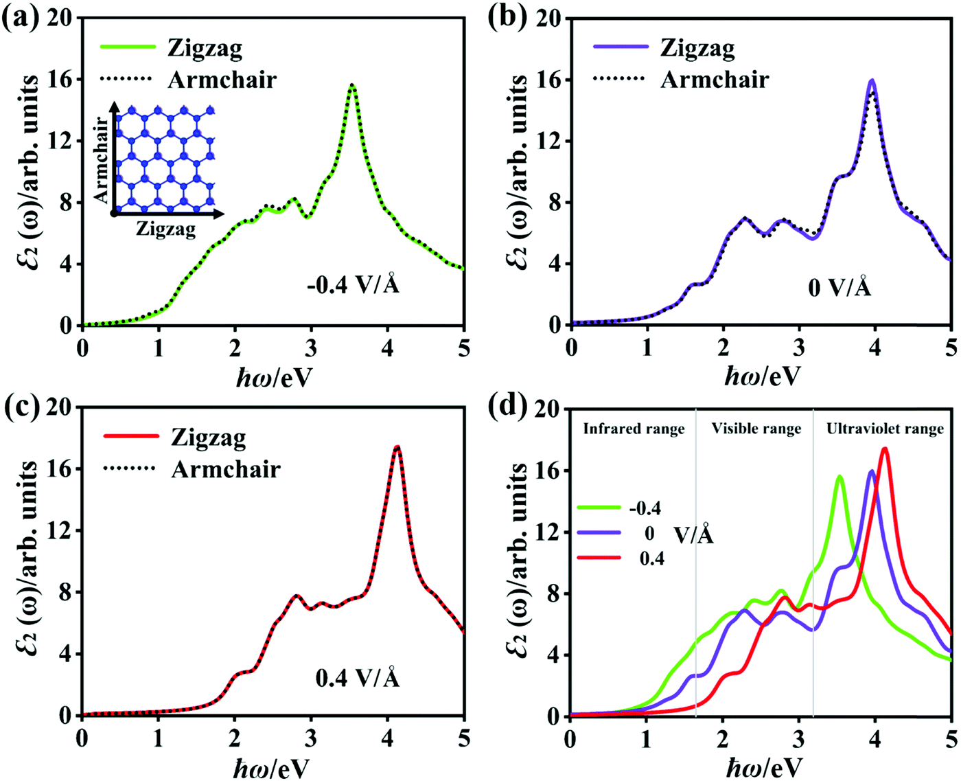 | ||
| Fig. 7 (a)–(c) The optical absorption spectra of the P2/MoSe2 vdW herterostructure along the two polarized-light directions (Zigzag and Armchair) at the vertical electric fields of −0.4 V Å−1, 0 V Å−1, and 0.4 V Å−1. The Zigzag and Armchair directions are inset. These calculated spectra have included the electron–hole interaction. (d) The comparable optical absorption spectra along the zigzag polarized-light direction (i.e. the a-axial direction) under different electric fields. A Lorentzian broadening of 0.15 eV is applied in the calculations of the optical spectra. | ||
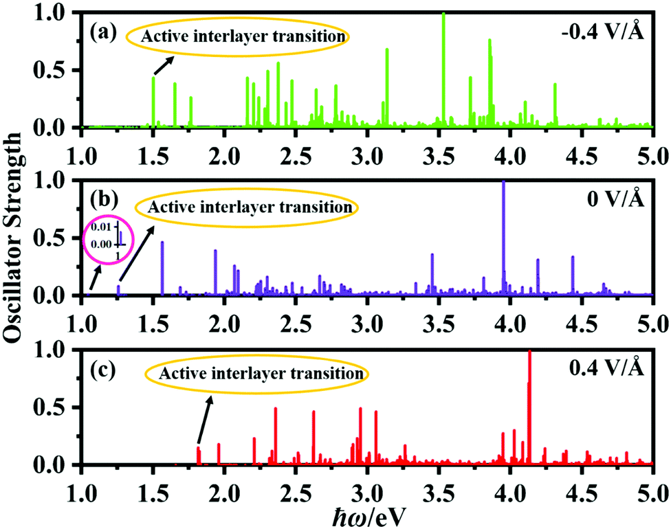
Fig. 8 shows the calculated oscillator strengths of the excited states of the P2/MoSe2 vdW herterostructure under the electric field of −0.4 V Å−1, 0 V Å−1, and 0.4 V Å−1, suggesting that the vertical electric field can significantly influence the photoexcited behavior of P2/MoSe2. Based on the oscillator strength selection rules, we analyze the transition of P2/MoSe2 under the three electric fields. For the primitive P2/MoSe2 vdW heterostructure, the low-energy spectrum of 0–2 eV is mainly contributed by the MoSe2 layer (as seen in Fig. 3(d)), which means that the intralayer excitons of the MoSe2 layer dominate the low-energy spectrum. However, an active interlayer transition is also found at the energy position of about 1.26 eV, which comes from the vertical transition between the VBM and CBM at certain non-high-symmetric point T(5/18, 1/3, 0) near high-symmetric K point. The partial charge distributions of VBM and CBM at the T point can be found in Fig. S7 (ESI†), in which the VBM (CBM) is mainly contributed by the MoSe2 (P2) layer. Another inactive interlayer transition is also observed at about 1.05 eV although its oscillator strength is very small (as seen in the inset of Fig. 8(b)), which is mainly between the VBM and CBM at the K point. The active interlayer transition can induce the formation of an interlayer exciton (i.e. indirect exciton), whose binding energy is estimated to be 670 meV by the method of the energy difference between the quasi-particle energy and excitation energy. For the cases of −0.4 V Å−1 and 0.4 V Å−1, active interlayer transitions occur at 1.50 eV and 1.82 eV, respectively (marked in Fig. 8(a) and (c)), which generate two corresponding interlayer excitons. For the −0.4 V Å−1, the active interlayer transition comes from the vertical transition between the VBM (MoSe2 layer) and CBM (P2 layer) at the K point, which is different to that of the primitive P2/MoSe2, while the active interlayer transition under the electric field of 0.4 V Å−1 is from the VBM (MoSe2 layer) to the second conduction band (P2 layer) at the K point. The two observed interlayer excitons also possess considerable binding energies of 614 meV for −0.4 V Å−1 and 628 meV for 0.4 V Å−1, which is comparable with that of the primitive P2/MoSe2. These interlayer excitons found in the P2/MoSe2 heterostructure are beneficial to facilitate the separation of photoexcited carriers, which is very important for applications in photovoltaics and photocatalytic water splitting. On the basis of the above results, we can draw a conclusion that the bandgap of the P2/MoSe2 vdW heterostructure can be modulated in a broad range and its optical properties can also be tuned effectively by applying the vertical electric field.
 | ||
| Fig. 8 (a)–(c) Calculated oscillator strengths of excited states of the P2/MoSe2 vdW herterostructure in the energy range of 1–5 eV for vertical electric fields of −0.4 V Å−1, 0 V Å−1, and 0.4 V Å−1. The polarized light is along the zigzag direction. | ||
4 Conclusions
In summary, we performed first-principles calculations to investigate the effect of vertical electric field on the electronic and optical properties of the constructed P2/MoSe2 vdW heterostructure. We found that the AA-stacking P2/MoSe2 with more stability has an intrinsic type-II band alignment, in which photoexcited electrons (holes) migrate from the MoSe2 (P2) to the P2 (MoSe2) layer. The estimated quasi-particle bandgap can be tuned effectively from 0.94 eV (−0.4 V Å−1) to 2.05 eV (0.4 V Å−1) by the vertical electric field. A transition from type-II to type-I can be observed under a moderate electric field of 0.24 V Å−1. More interestingly, P2/MoSe2 possesses a strong and broad optical absorption ranging from the near-infrared to near-ultraviolet. Under the negative electric field, the optical absorption of the P2/MoSe2 heterostructure for the visible and near-infrared light can be enhanced significantly. The active interlayer excitons with binding energy more than 600 meV are observed under the applied vertical electric field, being favorable to effectively separate the photoexcited electron–hole pairs. The electric field-tunable electronic and optical properties of the P2/MoSe2 vdW heterostructure make it a potential candidate for optoelectronic devices.Conflicts of interest
There are no conflicts to declare.Acknowledgements
This work is supported by the Research Fund (No. 1052931610) of Jiangsu University of Science and Technology.References
- C. V. Nguyen, M. Idrees, H. V. Phuc, N. N. Hieu, N. T. T. Binh, B. Amin and T. V. Vu, Phys. Rev. B, 2020, 101, 235419 CrossRef CAS.
- T. V. Vu, N. V. Hieu, H. V. Phuc, N. N. Hieu, H. D. Bui, M. Idrees, B. Amin and C. V. Nguyen, Appl. Surf. Sci., 2020, 507, 145036 CrossRef CAS.
- I. Shahid, S. Ahmad, N. Shehzad, S. Yao, C. V. Nguyen, L. Zhang and Z. Zhou, Appl. Surf. Sci., 2020, 523, 146483 CrossRef CAS.
- S. Fan, Q. A. Vu, M. D. Tran, S. Adhikari and Y. H. Lee, 2D Mater., 2020, 7, 022005 CrossRef.
- Q. Lv and R. Lv, Carbon, 2019, 145, 240–250 CrossRef CAS.
- K. S. Novoselov, A. Mishchenko, A. Carvalho and A. H. Castro Neto, Science, 2016, 353, aac9439 CrossRef CAS PubMed.
- H. Lim, S. I. Yoon, G. Kim, A.-R. Jang and H. S. Shin, Chem. Mater., 2014, 26, 4891–4903 CrossRef CAS.
- A. K. Geim and I. V. Grigorieva, Nature, 2013, 499, 419 CrossRef CAS PubMed.
- X. Hong, J. Kim, S.-F. Shi, Y. Zhang, C. Jin, Y. Sun, S. Tongay, J. Wu, Y. Zhang and F. Wang, Nat. Nanotechnol., 2014, 9, 682 CrossRef CAS PubMed.
- Q. Zheng, W. A. Saidi, Y. Xie, Z. Lan, O. V. Prezhdo, H. Petek and J. Zhao, Nano Lett., 2017, 17, 6435–6442 CrossRef CAS PubMed.
- X. Niu, Y. Li, Y. Zhang, Q. Zheng, J. Zhao and J. Wang, J. Mater. Chem. C, 2019, 7, 1864–1870 RSC.
- P. Rivera, J. R. Schaibley, A. M. Jones, J. S. Ross, S. Wu, G. Aivazian, P. Klement, K. Seyler, G. Clark, N. J. Ghimire, J. Yan, D. G. Mandrus, W. Yao and X. Xu, Nat. Commun., 2015, 6, 6242 CrossRef CAS PubMed.
- B. Miller, A. Steinhoff, B. Pano, J. Klein, F. Jahnke, A. Holleitner and U. Wurstbauer, Nano Lett., 2017, 17, 5229–5237 CrossRef CAS PubMed.
- L. Britnell, R. M. Ribeiro, A. Eckmann, R. Jalil, B. D. Belle, A. Mishchenko, Y.-J. Kim, R. V. Gorbachev, T. Georgiou, S. V. Morozov, A. N. Grigorenko, A. K. Geim, C. Casiraghi, A. H. C. Neto and K. S. Novoselov, Science, 2013, 340, 1311–1314 CrossRef CAS PubMed.
- Y. Deng, Z. Luo, N. J. Conrad, H. Liu, Y. Gong, S. Najmaei, P. M. Ajayan, J. Lou, X. Xu and P. D. Ye, ACS Nano, 2014, 8, 8292–8299 CrossRef CAS PubMed.
- P. Xiong, X. Zhang, H. Wan, S. Wang, Y. Zhao, J. Zhang, D. Zhou, W. Gao, R. Ma, T. Sasaki and G. Wang, Nano Lett., 2019, 19, 4518–4526 CrossRef CAS PubMed.
- Z. Yuan, J. Li, M. Yang, Z. Fang, J. Jian, D. Yu, X. Chen and L. Dai, J. Am. Chem. Soc., 2019, 141, 4972–4979 CrossRef CAS PubMed.
- Y.-T. Du, X. Kan, F. Yang, L.-Y. Gan and U. Schwingenschlögl, ACS Appl. Mater. Interfaces, 2018, 10, 32867–32873 CrossRef CAS PubMed.
- C. Zhao, C. Yu, B. Qiu, S. Zhou, M. Zhang, H. Huang, B. Wang, J. Zhao, X. Sun and J. Qiu, Adv. Mater., 2018, 30, 1702486 CrossRef PubMed.
- X. Wang, H. Li, H. Li, S. Lin, J. Bai, J. Dai, C. Liang, X. Zhu, Y. Sun and S. Dou, J. Mater. Chem. A, 2019, 7, 2291–2300 RSC.
- W. Liu, Z. Wang, Y. Su, Q. Li, Z. Zhao and F. Geng, Adv. Energy Mater., 2017, 7, 1602834 CrossRef.
- L. Huang, N. Huo, Y. Li, H. Chen, J. Yang, Z. Wei, J. Li and S.-S. Li, J. Phys. Chem. Lett., 2015, 6, 2483–2488 CrossRef CAS PubMed.
- N. Lu, H. Guo, L. Li, J. Dai, L. Wang, W.-N. Mei, X. Wu and X. C. Zeng, Nanoscale, 2014, 6, 2879 RSC.
- L. Huang and J. Li, Appl. Phys. Lett., 2016, 108, 083101 CrossRef.
- D. Chen, X. Lei, Y. Wang, S. Zhong, G. Liu, B. Xu and C. Ouyang, Appl. Surf. Sci., 2019, 497, 143809 CrossRef.
- K. Rahimi, Phys. Chem. Chem. Phys., 2020, 22, 7412–7420 RSC.
- S. Gao, L. Yang and C. D. Spataru, Nano Lett., 2017, 17, 7809–7813 CrossRef CAS PubMed.
- Y. Li, J.-K. Qin, C.-Y. Xu, J. Cao, Z.-Y. Sun, L.-P. Ma, P. A. Hu, W. Ren and L. Zhen, Adv. Funct. Mater., 2016, 26, 4319–4328 CrossRef CAS.
- S. Tongay, J. Zhou, C. Ataca, K. Lo, T. S. Matthews, J. Li, J. C. Grossman and J. Wu, Nano Lett., 2012, 12, 5576–5580 CrossRef CAS PubMed.
- J. S. Ross, S. Wu, H. Yu, N. J. Ghimire, A. M. Jones, G. Aivazian, J. Yan, D. G. Mandrus, D. Xiao, W. Yao and X. Xu, Nat. Commun., 2013, 4, 1474 CrossRef.
- M. Bernardi, M. Palummo and J. C. Grossman, Nano Lett., 2013, 13, 3664–3670 CrossRef CAS PubMed.
- B. Chamlagain, Q. Li, N. J. Ghimire, H.-J. Chuang, M. M. Perera, H. Tu, Y. Xu, M. Pan, D. Xaio, J. Yan, D. Mandrus and Z. Zhou, ACS Nano, 2014, 8, 5079–5088 CrossRef CAS PubMed.
- J. L. Zhang, S. Zhao, C. Han, Z. Wang, S. Zhong, S. Sun, R. Guo, X. Zhou, C. D. Gu, K. D. Yuan, Z. Li and W. Chen, Nano Lett., 2016, 16, 4903–4908 CrossRef CAS PubMed.
- J. Guan, Z. Zhu and D. Tománek, Phys. Rev. Lett., 2014, 113, 046804 CrossRef PubMed.
- Z. Zhu and D. Tománek, Phys. Rev. Lett., 2014, 112, 176802 CrossRef PubMed.
- B. Ghosh, S. Nahas, S. Bhowmick and A. Agarwal, Phys. Rev. B: Condens. Matter Mater. Phys., 2015, 91, 115433 CrossRef.
- J. Xiao, M. Long, X. Zhang, J. Ouyang, H. Xu and Y. Gao, Sci. Rep., 2015, 5, 9961 CrossRef CAS PubMed.
- A. Ramasubramaniam, Phys. Rev. B: Condens. Matter Mater. Phys., 2012, 86, 115409 CrossRef.
- D. Kozawa, A. Carvalho, I. Verzhbitskiy, F. Giustiniano, Y. Miyauchi, S. Mouri, A. H. Castro Neto, K. Matsuda and G. Eda, Nano Lett., 2016, 16, 4087–4093 CrossRef CAS PubMed.
- E. M. Alexeev, D. A. Ruiz-Tijerina, M. Danovich, M. J. Hamer, D. J. Terry, P. K. Nayak, S. Ahn, S. Pak, J. Lee, J. I. Sohn, M. R. Molas, M. Koperski, K. Watanabe, T. Taniguchi, K. S. Novoselov, R. V. Gorbachev, H. S. Shin, V. I. Fal’ko and A. I. Tartakovskii, Nature, 2019, 567, 81–86 CrossRef CAS PubMed.
- P. K. Nayak, Y. Horbatenko, S. Ahn, G. Kim, J.-U. Lee, K. Y. Ma, A.-R. Jang, H. Lim, D. Kim, S. Ryu, H. Cheong, N. Park and H. S. Shin, ACS Nano, 2017, 11, 4041–4050 CrossRef CAS PubMed.
- S. Goedecker, M. Teter and J. Hutter, Phys. Rev. B: Condens. Matter Mater. Phys., 1996, 54, 1703–1710 CrossRef CAS PubMed.
- P. Giannozzi, S. Baroni, N. Bonini, M. Calandra, R. Car, C. Cavazzoni, D. Ceresoli, G. L. Chiarotti, M. Cococcioni, I. Dabo, A. Dal Corso, S. de Gironcoli, S. Fabris, G. Fratesi, R. Gebauer, U. Gerstmann, C. Gougoussis, A. Kokalj, M. Lazzeri, L. Martin-Samos, N. Marzari, F. Mauri, R. Mazzarello, S. Paolini, A. Pasquarello, L. Paulatto, C. Sbraccia, S. Scandolo, G. Sclauzero, A. P. Seitsonen, A. Smogunov, P. Umari and R. M. Wentzcovitch, J. Phys.: Condens. Matter, 2009, 21, 395502 CrossRef PubMed.
- J. P. Perdew, K. Burke and M. Ernzerhof, Phys. Rev. Lett., 1996, 77, 3865–3868 CrossRef CAS PubMed.
- M. Dion, H. Rydberg, E. Schröder, D. C. Langreth and B. I. Lundqvist, Phys. Rev. Lett., 2004, 92, 246401 CrossRef CAS PubMed.
- M. Dion, H. Rydberg, E. Schröder, D. C. Langreth and B. I. Lundqvist, Phys. Rev. Lett., 2005, 95, 109902 CrossRef.
- L. Bengtsson, Phys. Rev. B: Condens. Matter Mater. Phys., 1999, 59, 12301–12304 CrossRef CAS.
- S. Baroni, S. de Gironcoli, A. Dal Corso and P. Giannozzi, Rev. Mod. Phys., 2001, 73, 515–562 CrossRef CAS.
- L. Hedin, Phys. Rev., 1965, 139, A796–A823 CrossRef.
- E. E. Salpeter and H. A. Bethe, Phys. Rev., 1951, 84, 1232 CrossRef.
- M. Rohlfing and S. G. Louie, Phys. Rev. B: Condens. Matter Mater. Phys., 2000, 62, 4927–4944 CrossRef CAS.
- A. Marini, C. Hogan, M. Grüning and D. Varsano, Comput. Phys. Commun., 2009, 180, 1392–1403 CrossRef CAS.
- T. Böker, R. Severin, A. Müller, C. Janowitz, R. Manzke, D. Voß, P. Krüger, A. Mazur and J. Pollmann, Phys. Rev. B: Condens. Matter Mater. Phys., 2001, 64, 235305 CrossRef.
- M. M. Ugeda, A. J. Bradley, S.-F. Shi, F. H. da Jornada, Y. Zhang, D. Y. Qiu, W. Ruan, S.-K. Mo, Z. Hussain, Z.-X. Shen, F. Wang, S. G. Louie and M. F. Crommie, Nat. Mater., 2014, 13, 1091–1095 CrossRef CAS PubMed.
- A. J. Bradley, M. M. Ugeda, F. H. da Jornada, D. Y. Qiu, W. Ruan, Y. Zhang, S. Wickenburg, A. Riss, J. Lu, S.-K. Mo, Z. Hussain, Z.-X. Shen, S. G. Louie and M. F. Crommie, Nano Lett., 2015, 15, 2594–2599 CrossRef CAS PubMed.
- C. E. P. Villegas, A. S. Rodin, A. Carvalho and A. R. Rocha, Phys. Chem. Chem. Phys., 2016, 18, 27829–27836 RSC.
- The AM 1.5G Spectrum Was Taken from the NREL Website: http://Rredc.Nrel.Gov/Solar/Spectra/Am1.5 and Integrated with the Trapezoid Rule.
- Y. Gong, J. Lin, X. Wang, G. Shi, S. Lei, Z. Lin, X. Zou, G. Ye, R. Vajtai, B. I. Yakobson, H. Terrones, M. Terrones, B. K. Tay, J. Lou, S. T. Pantelides, Z. Liu, W. Zhou and P. M. Ajayan, Nat. Mater., 2014, 13, 1135–1142 CrossRef CAS PubMed.
- B.-J. Wang, X.-H. Li, R. Zhao, X.-L. Cai, W.-Y. Yu, W.-B. Li, Z.-S. Liu, L.-W. Zhang and S.-H. Ke, J. Mater. Chem. A, 2018, 6, 8923–8929 RSC.
- B.-J. Wang, X.-H. Li, X.-L. Cai, W.-Y. Yu, L.-W. Zhang, R.-Q. Zhao and S.-H. Ke, J. Phys. Chem. C, 2018, 122, 7075–7080 CrossRef CAS.
- N. A. Lanzillo, A. J. Simbeck and S. K. Nayak, J. Phys.: Condens. Matter, 2015, 27, 175501 CrossRef PubMed.
- F. Ceballos, M. Z. Bellus, H.-Y. Chiu and H. Zhao, ACS Nano, 2014, 8, 12717–12724 CrossRef CAS PubMed.
- S. Tongay, W. Fan, J. Kang, J. Park, U. Koldemir, J. Suh, D. S. Narang, K. Liu, J. Ji, J. Li, R. Sinclair and J. Wu, Nano Lett., 2014, 14, 3185–3190 CrossRef CAS PubMed.
- M.-H. Chiu, M.-Y. Li, W. Zhang, W.-T. Hsu, W.-H. Chang, M. Terrones, H. Terrones and L.-J. Li, ACS Nano, 2014, 8, 9649–9656 CrossRef CAS PubMed.
Footnote |
| † Electronic supplementary information (ESI) available. See DOI: 10.1039/d0ma00413h |
| This journal is © The Royal Society of Chemistry 2020 |