
 Open Access Article
 This Open Access Article is licensed under a
 Creative Commons Attribution 3.0 Unported Licence
Room-temperature application of VO2 microstructures on rigid and flexible substrates based on synthesis of crystalline VO2 solution†
Mohammad
Taha
 *ab,
Edwin L. H.
Mayes
c,
Matthew R.
Field
c,
Miao
Sun
a,
Mandeep
Singh
d and
Wenyue
Zou
d
*ab,
Edwin L. H.
Mayes
c,
Matthew R.
Field
c,
Miao
Sun
a,
Mandeep
Singh
d and
Wenyue
Zou
d
aDepartment of Electrical and Electronic Engineering, School of Engineering, The University of Melbourne, Parkville, VIC 3010, Australia. E-mail: mohammad.taha@unimelb.edu.au
bRMIT University, Melbourne, VIC 3000, Australia
cRMIT Microscopy & Microanalysis Facility, College of Science, Engineering and Health, RMIT University, Melbourne, VIC 3000, Australia
dIan Potter NanoBioSensing Facility, NanoBiotechnology Research Laboratory, School of Science, RMIT University, Melbourne, VIC 3000, Australia
First published on 9th September 2020
Abstract
The insulator-to-metal transition (IMT) in vanadium dioxide (VO2) offers temperature-dependent infrared wavelength attenuation, rendering it a great contender for bolometers, optoelectronics, memory devices, smart-windows adaptive thermal camouflage applications. However, the required high temperature processing (up to 600 °C) of VO2 inhibits its widespread utilization, particularly in applications with low fabrication temperature limits – such as devices on flexible polymer substrates. This study provides a new method that relies on van der Waals substrates with inert basal planes and hydrophilic surfaces to overcome the hurdle of high processing temperatures. Using this method, highly-oriented, optically active crystalline VO2 was deposited on both glass and flexible polyethylene terephthalate (PET) substrates. We observe VO2 crystals during IMT using transmission electron microscopy (TEM), X-ray photoelectron spectroscopy (XPS) and report >60% change in transmission on both glass and flexible PET, as well as demonstrating IR modulation.
Introduction
With ever-increasing global energy demands and continuously worsening climate conditions, it is paramount to develop more sophisticated energy solutions, and to not only rely on renewable energy but to also mitigate excessive energy losses and minimize redundancy. Windows are considered to be a significant source of energy loss in buildings and other structures. Heating and cooling of buildings accounts for ∼14% of the total energy use in the US.1 Therefore, reducing unnecessary energy loss from buildings is a vital part of the roadmap towards a sustainable future economy. Minimizing energy loss through windows may be achieved through thermally responsive glazing and coatings, which are an emerging and vital parts of glass technology.2 Dynamic windows, or smart-windows, change their optical properties by utilizing materials that feature photochromism, electrochromism or thermochromism to overcome the traditionally wasteful nature of windows.3Monoclinic vanadium dioxide (VO2) is both electrochromic and thermochromic, and is thus suitable to be applied in smart dynamic coatings,4–6 since it simultaneously blocks ultraviolet (UV) radiation and modulates infrared (IR) light.7–11 Crystalline VO2 experiences thermochromism at ∼68 °C, when the material switches from a semiconducting monoclinic to a conductive tetragonal configuration. As the material changes crystal configuration, it experiences an increase in free charge carriers, leading to a metallic state. Metallic VO2 exhibits a dramatically reduced transmission in the IR, microwave and terahertz wavelengths range when compared to the semiconducting phase.12–18 The insulator-to-metal transition (IMT) of vanadium oxides depends on the microstructure, morphology and stoichiometry of the oxide. The transition generally occurs within pico/femtoseconds,19 making vanadium oxide a promising candidate for electronic switch components in integrated circuits,20 smart window coatings,21–23 tunable antennas24,25 and metamaterials.26
However, the development of commercially viable synthesis methods for VO2 is hindered, due to inherent difficulties associated with the existence of vanadium oxides of different stoichiometry and pronounced polymorphism. With 15–20 other stable vanadium oxide phases, the formation of VO2 occurs only over specific ranges of oxygen partial pressures and temperatures.27,28 Therefore, vapor phase VO2 synthesis methods such as sputtering29–34 and chemical-vapor deposition (CVD)35–38 are widely employed, since they offer a high degree of control over the partial oxygen pressure and can be operated at high temperatures.
Solution-based methods such as sol–gel10,39,40 and polymer assisted deposition (PAD)40,41 have also been reported. These methods utilize chemical precursors dissolved in a liquid medium. Such synthesis techniques result in colloidal suspensions, which are excellent for coating large areas using solution processing; however, they still pose limitations on the application of VO2 solution to temperature-sensitive surfaces and fabrics, since solutions do not undergo IMT without a subsequent annealing step. As a result, they are not suitable for application in a large number of thermally unstable existing window technologies (i.e. acrylic windows) or the retrofitting of existing windows or integration with flexible substrates with low melting points, or fabrics. Importantly, even though hydrothermal processes are widely used in VO2 synthesis, they do not benefit from the level of morphological and crystallographic control available when using physical or chemical vapor deposition techniques.
Herein, we report a two-step fabrication method that allows the synthesis of fully-functional VO2 using physical vapor deposition (PVD) techniques. The VO2 can then be suspended to create a functional colloidal ink that can be applied to any surface, without the need for further post-application annealing. We use highly hydrophilic mica growth substrates to develop this technology, enabling the highly-oriented growth of crystalline VO2 films through pulsed-DC magnetron sputtering,42–44 while allowing the lift-off into solution post-synthesis. We characterize the VO2 suspension and observe IMT using in situ transmission electron microscopy (TEM), selected area electron diffraction (SAED) and X-ray photoelectron spectroscopy (XPS), before introducing VO2 to standard glass and a flexible substrate with low thermal stability (PET) for optical characterization.
Experimental section
VO2 solution synthesis
The VO2 thin films are deposited onto mica using pulsed DC magnetron sputtering technique. A vanadium target (99.98% purity) was set up at ∼120 mm from the substrates with base pressure of ∼4 × 10⁻⁷ and working pressure of ∼3 × 10⁻³. The Ar![[thin space (1/6-em)]](https://www.rsc.org/images/entities/char_2009.gif) :O2 flow rate of the gas mixture in the sputtering chamber was 13.25:6.25 sccm. Sputtering was conducted at 200 W with pulse frequency and reverse time at 25 kHz and 5 μs respectively. VO2 films were then annealed in a furnace, and evacuated to low vacuum to achieve a pressure of ∼50–150 mTorr, at 550°C for 90min. Mica coated with crystalline VO2 was immersed in water to allow for delamination (sonication was not essential, but it expediates the delamination of VO2 crystals). The resultant solution was placed in an oven to undergo slow evaporation overnight at 90 °C, before being allowed to cool down to room temperature. IPA was added to the crystals, forming a VO2 solution that can be evaporated at room temperature.
:O2 flow rate of the gas mixture in the sputtering chamber was 13.25:6.25 sccm. Sputtering was conducted at 200 W with pulse frequency and reverse time at 25 kHz and 5 μs respectively. VO2 films were then annealed in a furnace, and evacuated to low vacuum to achieve a pressure of ∼50–150 mTorr, at 550°C for 90min. Mica coated with crystalline VO2 was immersed in water to allow for delamination (sonication was not essential, but it expediates the delamination of VO2 crystals). The resultant solution was placed in an oven to undergo slow evaporation overnight at 90 °C, before being allowed to cool down to room temperature. IPA was added to the crystals, forming a VO2 solution that can be evaporated at room temperature.
X-ray photoelectron spectroscopy (XPS) and X-ray diffraction (XRD)
XPS analysis was conducted using a Thermo Scientific K-Alpha instrument under ultrahigh vacuum (base pressure <1 × 10⁻⁷Pa). An aluminum Kα X-ray radiation source with energy of 1486.6eV was used. All core-level spectra of the elements were collected at pass energy of 50eV and analyzed with Advantage software. The binding energies of all principal elements were referenced to the adventitious carbon (C 1s) of binding energy 284.6eV. XRD diffractograms are produced using X-ray diffraction powder analyser (D2 Phaser, Bruker).
UV-Vis and bandgap measurements
The UV-Vis absorbance measurements of the aqueous suspension of VO2 were carried out using an Agilent Cary 7000 UV-Vis-NIR spectrophotometer equipped with an integrating sphere.Raman spectroscopy
Raman spectra were acquired on a Horiba LabRAM HR Evolution Raman spectrometer using a 532nm laser with 0.5 mW power and Magnification during the experiment was set to ×100. In this experiment, pure Si was used as substrates.
Scanning electron microscopy (SEM)
The FEI Verios 460L was used to collect scanning electron micrographs. Samples were coated with 5 nm of Pt before being placed in the chamber to prevent surface discharge. FEI Helios Nanolab 600 Dual Beam FIB-SEM was used to collect micrographs of cross sections of VO2 microstructures on glass.In situ transmission electron microscopy (TEM) and electron energy-loss spectroscopy (EELS)
TEM and EELS measurements were collected by drop-casting VO2 crystals onto a Protochips heating chip and mounting it in a Fusion heating/biasing sample holder. TEM in situ analysis for diffraction and imaging were then performed on a JEOL 2100F TEM operating at 200 kV. The following parameters were used (Spot size = 1, alpha = 3, condenser aperture number 3 (CA3), selected area aperture number 2 (SA2)) and the flake was fully covered during the experiment. EELS analysis was performed using the same sample and holder combination in a JEOL F200 TEM operating at 200 kV in STEM mode. A Gatan Continuum S spectrometer was used to collect core loss V L2,3 edge spectra.Data was collected at initially conditions (∼22 °C) and again at elevated temperature (120 °C) to ensure the transition from the M1 monoclinic phase to the tetragonal phase had completed. As the transition is fully reversible, several temperature sweeps were collected for each data type and for video of the transition process.
In situ X-ray photoelectron spectroscopy (XPS)
XPS with in situ heating was performed using a Kratos Axis Supra with monochromated Al Kα X-ray source (1486.6 eV) operated at 30 mA emission. The samples were pre-cleaned using 5 s of 2 keV Ar1000 gas cluster ion sputtering.Optical measurements
UV-Vis-IR transmission spectra were collected using a CRAIC 20/30 microspectrophotometer. A custom-made stage was used to conduct in situ measuring transmission through the samples. Optical transmission values were collected and recorded at different temperature to observe thermochromic behaviour of the microstructures.Infrared imaging
Temperature was measured by placing the samples and the control on a hot plate and taking infrared images using the FLIR C2 education kit.VO2 optical transmission simulation
VO2 crystal drop-cast on a quartz substrate was carried out using the finite element method implemented in COMSOL Multiphysics. The simulation model consists of 1 μm thick layer of a semi-infinite glass substrate with the refractive index value, 1.5. The refractive indices of quartz for different wavelengths were taken from COMSOL embedded material library. A VO2 crystal layer with different size of flakes was added on the top of the quartz substrate. The thickness of VO2 was set to 80 nm due to the average measurement under FIB to study its effect on transmission and switching on the semiconductor phase and metallic phase. A 1.5 μm air superstrate was constructed on the top of VO2 section. To simulate a large area of VO2 drop, periodic boundary condition was applied on four sides of the model. The incident light was set to propagate along the perpendicular to the substrate surface with TE polarization using port boundary condition. A 300 nm Perfect match layer (PML) was added to the top boundary and the bottom boundary to absorb the outgoing wave and to ensure that no reflection was present in the interior region.Results and discussion
Synthesis of crystalline VO2 solution
VO2 are deposited directly on mica substrates using pulsed-DC magnetron sputtering at room-temperature for 45 minutes in (O2:Ar) ratio of 30%, leading to films with a thickness of ∼150 nm. The amorphous films undergo crystallization as the films are annealed in partial air at 550 °C for 90 minutes in a vacuum furnace with a pressure between 50–150 mTorr. Subsequently, the grown films are immersed and sonicated in water to separate the functional VO2 crystals from the mica substrates. Mica is a naturally stratified van der Waals material that features chemically inert basal planes, leading to the grown VO2 being primarily attached to the surface via weak van der Waals forces. During the delamination process, water intercalates the VO2–mica interface, while the mica basal plane experiences H-bonding with H2O, donating H+ to the interface, leading to the delamination of PVD-grown VO2 crystals.45 As an increasing number of crystals are released from the surface, more H-bonding occurs, which in turn leads to more rapid separation and ultimately the effective delamination of the grown VO2 from the mica surface. Delaminated VO2 is introduced into isopropyl alcohol (IPA) to enable rapid room-temperature drying before being drop-cast on glass and polyethylene terephthalate (PET) substrates for characterization. Fig. 1a–f visualizes the synthesis process leading to highly oriented crystalline VO2, and the mechanism of separation from the mica substrate. An image of the VO2 suspension is shown in the ESI,† in Fig. S1.
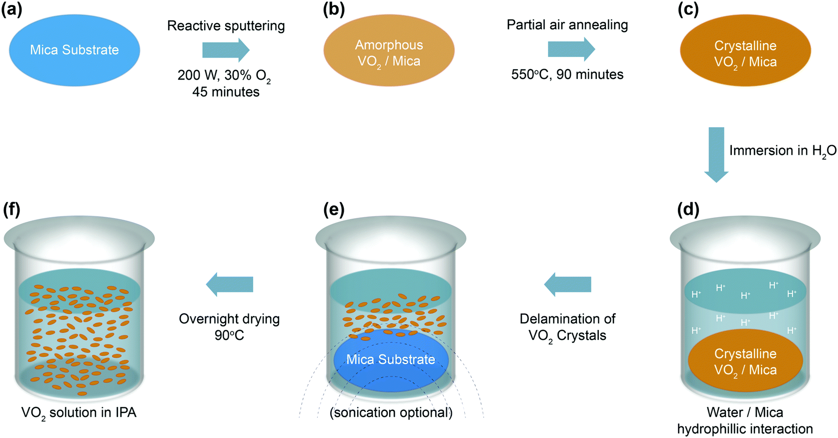 | ||
| Fig. 1 Synthesis of VO2 in isopropyl alcohol (IPA). (a) Preparing clean mica substrates by removing the top sheet of the mica substrate to avoid impurities before film synthesis. (b) Amorphous VO2 thin film deposition using pulsed-DC magnetron sputtering for 45 minutes at ambient temperature using 200 W power and 30% oxygen. (c) Post-deposition annealing and crystallization in partial air with working pressure of ∼50–150 mTorr for 90 minutes. (d) Immersion of VO2/mica in water. (e) Delamination of VO2 crystals due to mica basal plane experiencing H-bonding with H2O, separating VO2 crystals from the substrate. After delamination is complete the mica substrate is removed from water. (f) Slow water evaporation overnight at 90 °C to ensure minimal changes to crystallinity and composition, and solvent (IPA) addition to assist in rapid drying of the solvent at room temperature. | ||
Composition, optical bandgap, Raman spectra and surface morphology of VO2 crystals
The two-step process reported here includes suspending VO2 microstructures first in water, then in isopropyl alcohol (IPA). Consequently, it is of great importance to verify that the synthesized VO2 crystals maintain their stoichiometry and functionality, and do not undergo chemical reactions while being suspended. X-ray photoelectron spectroscopy (XPS) was used to detect any possible changes to the stoichiometry and bonding of the oxygen and vanadium atoms. Fig. S2 (ESI†) shows the XPS survey scan of the VO2 microstructures synthesised for elemental analysis. The presence V 2p, O 1s peaks and high energy core level peaks OKLL confirms the presence of all the composing elements. Fig. 2a and b show the vanadium and oxygen core-level XPS before and after the separation from the mica substrate. The samples exhibit a V 2p3/2 peak at ∼516.4 eV, which is associated with vanadium in the V4+ oxidation state.46–53 The O 1s peaks at ∼530 eV corresponds to V–O bonding, as indicated in the literature,46,50,54 while 532 eV corresponds to oxygen atoms in the Si–O in the substrate.55 These findings confirm that the grown crystals as well as the delaminated samples that have been drop-cast on glass substrates for analysis are indeed VO2. Overall, aside from the Si–O peak in the drop-cast VO2, binding energies and oxidation states correlate well, indicating that the composition of VO2 crystals withstands the delamination process.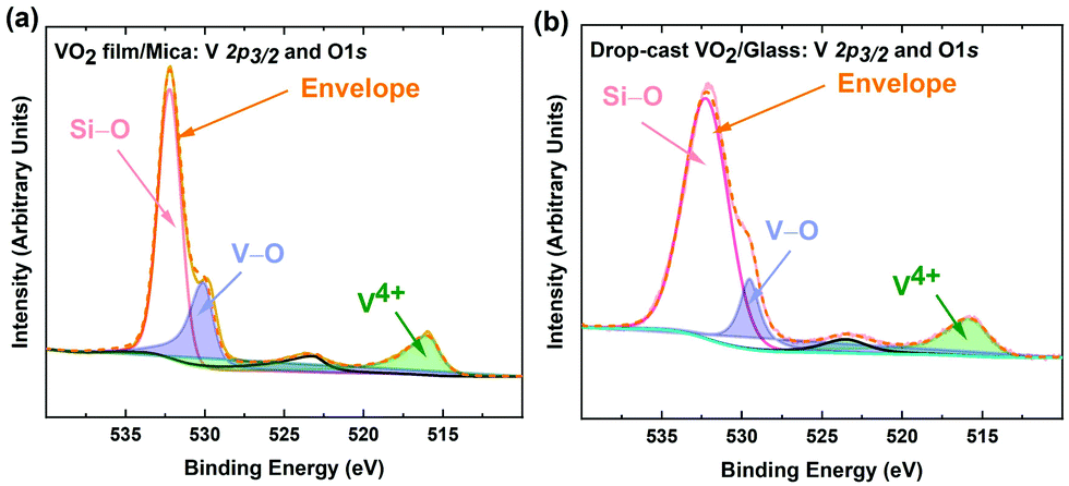 | ||
| Fig. 2 XPS spectra of vanadium (V 2p3/2) and oxygen (O 1s) for (a) VO2 films on mica and (b) drop-cast VO2 on glass, showing peaks at ∼530 and 532 eV (which indicate the V–O bonding and Si–O peak), and a peak at ∼516.4 eV (associated with vanadium in the V4+ oxidation). | ||
The optical properties of the synthesized VO2 solution were investigated utilizing solution-based UV-Vis spectroscopy. Fig. 3a inset shows the optical absorption spectrum of drop-cast VO2. Tauc plot analysis was performed to determine the optical bandgap of the synthesized material. Considering composition, oxidation state of vanadium and bulk crystallinity of VO2 in Fig. 3 a Tauc plot is a beneficial correlation in bandgap between VO2 synthesized here and reported pristine VO2 structures. The spectrum indicates that the crystals in solution are VO2, since the determined bandgap between V 3d‖ and 3π* of ∼0.72 eV is characteristic for pristine VO2,56–62 while other possible vanadium oxides such as V2O5 feature wider gaps of ∼2.35 eV.62,63 These measurements confirm that there are no other vanadium oxides present since the bandgap measures is characteristic to VO2. In Fig. 3a, a ∼1.95 eV bandgap is present between O 2pπ and V 3d‖, similar to literature reports.62 This bandgap is born to the admixture of vanadium and oxygen bands in VO2, however, this second bandgap is only slightly affected by IMT in VO2, since it remains intact while the V 3d‖ and 3π* bandgap collapses. The Raman spectrum of the synthesized VO2 crystals is shown in Fig. 3b. The observed vibrational modes at 285 and 407 cm−1 are associated with the V–O bending mode. The peak at ∼143 cm−1 corresponds to the Bg symmetry,64–66 while the peak at ∼97 cm−1 is indicative of a two dimensional (2D) layered architecture, since this mode arises from the translated neighboring layers.67–75 The peak at ∼520 cm−1 can be attributed to the silicon substrate that was used during the measurement.76 Other phonon modes at 195 (Ag), 225 (Ag), 304 (Ag), 439 (Bg), 615 (Ag) and 700 cm−1 wavenumbers are reported VO2 phonon vibrations.70–75
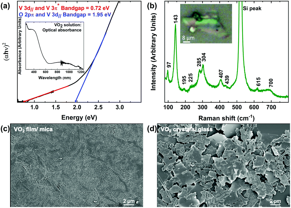 | ||
| Fig. 3 (a) A plot of (αhν)2versus photon energy for VO2 solution. Red line shows extrapolation to the (αhν)2 = 0, indicating the optical energy gap EOptg and optical absorbance. The blue line shows a second bandgap, which is born to the admixture of vanadium and oxygen bands in VO2. (b) Raman spectra for VO2 crystals on glass with an optical microscope image of a VO2 crystal. SEM image (15000× magnification) are shown for (c) VO2 film on mica, and (d) VO2 crystals on glass, highlighting the difference in morphology and crystal structure between VO2 thin film on mica before delamination and VO2 microstructures after the delamination process. | ||
Fig. S3a and b (ESI†) show the X-ray diffraction (XRD) diffractograms for the microstructures before and after the delamination process. Fig. S3a (ESI†) is dominated by the peaks of the mica crystal77 and due to the potential overlap with the diffraction features of the substrate mica crystals and VO278–80 XRD could not be used to unambiguously analyse the crystal microstructure of the VO2 crystals structure. Without further steps to remove all mica, some is unavoidably transferred into solution alongside the VO2; however, it is unlikely to affect the optical properties of the solution processed VO2 due to the wide bandgap and the absence of IMT in mica. Henceforth, in depth analysis to in situ transmission electron microscopy (TEM), selected area electron diffraction (SAED), electron energy loss spectroscopy (EELS) and X-ray photoelectron microscopy (XPS) are relied upon to both examine and verify the monoclinic to tetragonal transition characteristic to VO2.
The scanning electron microscopy (SEM) image in Fig. 3c shows the VO2 thin film before the delamination process. The films show some uniformity, while the VO2 microstructures shown in Fig. 3d are non-uniform and have a different and varying morphology. As parts of the films break during delamination, comparisons in surface roughness using atomic force microscopy (AFM) are not effective, especially in the context of the development of crystalline VO2 solution. Fig. 3d confirms the layered nature of the VO2 crystals, revealing sheet sizes in the range of 0.5 to 10 μm. Particle morphology is observed to be not uniform, with substantial size and shape variation, while pinholes are prevalent. Cracking of the VO2 potentially originates during the manual handling of the mica substrate and diffusion-based delamination process that occurs when samples are immersed in water. Further SEM images displaying similar morphology are shown in the ESI† in Fig. S4a–f. The observed overall consistency in morphology between samples attests to the reproducible nature of the process.
In situ characterization of VO2 crystals
In situ transmission electron microscopy (TEM), selected area electron diffraction (SAED) and electron energy loss spectroscopy (EELS)
The microcrystalline and electronic structure of VO2 crystals during the temperature-induced transition were studied using high resolution transmission electron microscopy (HRTEM), selected area electron diffraction (SAED) and electron energy loss spectroscopy (EELS). HRTEM and SAED patterns were analyzed and interpreted utilizing Java Electron Microscopy Software (JEMS) simulations and SingleCrystal 4 software. The data used for analysis is shown in Fig. S5 (ESI†). Fig. 4a–c show HRTEM images of VO2 drop-cast on a heating chip during different stages of the IMT. The calculated lattice spacing of the VO2 crystal at room temperature (Fig. 4a) is ∼3.3 Å along the 〈110〉 axis, which is consistent with the monoclinic phase of VO2.81 The VO2 lattice was found to be highly oriented, and the SAED pattern shows a single crystal over the selected area, which attests to the high crystal quality of the synthesized VO2. As the temperature of the sample is increased (Fig. 4a–c), the morphological change of the VO2 crystals can be observed, leading to images (a) before, (c) during, and (b) after IMT. The dashed red circles in Fig. 4a–c highlight the edge of the crystal, where the change of the crystal phase from monoclinic to tetragonal coordination is particularly apparent through reversible change in contrast, which can be ascribed to change in phase (see ESI,† S5 Video Image 1). | ||
| Fig. 4 Transmission electron microscopy (TEM), high-resolution transmission electron microscopy (HRTEM) and selected area electron diffraction (SAED) pattern at: (a) room temperature (monoclinic VO2 phase [−2, 2, −3] zone) and (b) 120 °C (tetragonal VO2 phase [2, 3, 1] zone). (c) TEM at 100 °C. (d) Electron energy-loss spectroscopy (EELS) at room temperature (cyan) and 120 °C (purple). | ||
It is observed that both the surfaces and edges of the crystal It is observed that both the surfaces and edges of the crystal transition move through three distinct steps. The monoclinic state is observed at room temperature. During transition, the crystal is in a transient state, which is indicated by the dramatic difference in contrast between Fig. 4c and the structures in Fig. 4a and b. The low contrast observed in the transient state can arise from factors such as thermal fluctuation and boundary movement. Furthermore, it can indicate higher electron transmission through VO2 microstructures. With the contrast being the result of a higher degree of scattering caused by microstructures in motion in the less stable transient state during IMT. It is noteworthy that the crystal transition is possible to observe, even though it is reported that IMT in VO2 occurs in the order of pico/femtoseconds82 due to microstructures undergoing phase transition independently.83
The microstructural change in Fig. 4a–c is reversible, and this can be seen in Video Image 1 of the VO2 crystal transformation in the ESI.† It is also noted that the TEM heating chip is heated to 120 °C, even though VO2 IMT temperature is 68 °C. This ensured the entire heated area of the chip was at above the IMT transition temperature and would remain so for the duration of the required measurements. In the monoclinic states, diffraction patters at VO2 (−1, −1, 0), (1, 1, 0), (−3, 0, 2), (3, 0, −2), (−2, 1, 2), (2, −1, −2), (−1, 2, 2) and (1, −2, −2) are observed in addition to high-order Lau zone (HOLZ) reflection characteristic to monoclinic VO2. IMT as observed by electron diffraction is characterized by the disappearance of the reflection along the 〈011〉 axis in the tetragonal state in Fig. 4b and the emergence of diffraction patterns at VO2 (−1, 1, −1), (1, −1, 1), (−3, 2, 0), (3, −2, 0), (2, −1, −1), and (−2, 1, 1). This observation results from the rearrangement of VO2 microstructures into linear chains as the microstructures moves between the monoclinic and the tetragonal states. The insets in Fig. 4a and b show selected area electron diffraction (SAED) pattern before and after the transition. As expected, the patterns correspond to the monoclinic and tetragonal phases of VO2.53,84–86 The high switching speed of VO2 is more apparent in SAED video imaging as well as the in situ collection of SAED patterns, which are provided in the ESI,† S5 Video Image 2. Since microstructures undergo IMT independently, SAED patterns reflect a single microstructure during this process, and SAED patterns for the transient state are not possible to observe. The high switching speed of VO2 is distinguished in Video Image 2 (ESI†) through the unchanged timestamp (2:29:214) in the video image before and after IMT, which emphasizes that IMT switching is faster than the resolution the clock provides. The electronic structure of the VO2 crystal was investigated through in situ EELS measurements before and after IMT. Fig. 4d shows a typical VO2 EELS spectrum featuring the V-L3, V-L2 and O-K edge onset at 513, 521, 532 eV respectively, and atomic ratio of vanadium to oxygen of ∼2.0.87,88 The overall V-L3, V-L2 and O-K edge onset and atomic ratios in the insulating and the metallic states in Fig. 4d remains unchanged, since IMT in VO2 is a reversible change in electronic, structural and inter/intra band interactions. A subtle change in the electronic structure is observed, indicated by the broadening of the O-K onset in the insulating state. IMT impact on band interactions can be recognized since the O-K edge measures dipole-allowed core-hole interactions between the O 1s to unoccupied O 2p and the V 3d‖, due to the organization of O 2p in symmetries that allow the mixture of O 2p and V 3d states.89,90Fig. 4d highlights the differences in the O-K edge between insulating and metallic VO2. In the insulating state, V 3d‖* is unoccupied, displaying a lower electron energy loss that leads to a higher full width half maximum (FWHM) of 2.56. In contrast, V 3d‖* is merged with V 3d‖ and is occupied in the metallic state of VO2, causing it to generate a greater electron energy loss and a lower FWHM of 1.72. This change in the O-K edge indicates changes in the V 3d‖* band during IMT, and is congruent with similar literature reports.91In situ EELS measurements indicates the changes in the electronic structure to the V 3d‖* band in VO2 during IMT and in situ TEM and SAED observations conclusively verify that VO2 crystals undergo IMT with changes in morphology. Therefore, we can determine that VO2 crystals change in both electronic structure and morphology during phase change. However, more accurate in-depth analysis of band transitions and interactions requires the utilization of in situ X-ray photoelectron spectroscopy (XPS).
In situ X-ray photoelectron microscopy (XPS)
In a monoclinic VO2 crystal system, the V 3d‖ splits into two energy bands, V 3d‖ and V 3d‖*, and the insulating forbidden band of ∼0.7 eV between V 3dπ* and V 3d‖ is formed. When VO2 undergoes IMT, the forbidden band collapses and the V 3d‖ band extends into the conduction band, forming the metallic tetragonal VO2 crystal system.60,92Consequently, valence band XPS can be used to observe the shift in the V 3d band to the Fermi level when the IMT occurs and the band gap is collapsed. Fig. 5a shows XPS spectra of core-levels at 20 °C (room temperature) and after heating in situ to 120 °C. Symmetric broadening of the V 2p peaks by ∼1.5 eV is observed above the IMT temperature, which is in agreement with previous reports.47,93 The broadening is explained by the Coloumb attractive force between the V 2p core-hole and the localized electrons in the V 3d band at the Fermi level, which has been estimated to be 1.5 eV for VO2.94 The instantaneous interactions between the core-hole level and the valence band electrons lead to this artifact in the V 2p3/2 peak in the core-level spectrum. Fig. 5b shows the valence band spectra of the VO2 sample at 20 °C and 120 °C. A ∼0.7 eV prominent shift of the V 3d band towards the Fermi level can be observed (see inset Fig. 5b) after the collapse of the forbidden band.
 | ||
| Fig. 5 (a) X-ray photoelectron spectroscopy (XPS) of core-levels of VO2 microstructures at 20 °C (cyan) and 120 °C (red) showing broadening of the V 2p by 1.5 eV. (b) Valence band spectra of VO2 microstructures at 20 °C (cyan) and 120 °C (red). The enlarged inset shows shift in the V 3d band by 0.66 eV. | ||
IMT in VO2 microstructures on glass, flexible substrates and thermal attenuation
After verifying IMT behavior using in situ characterizations of VO2 crystals, the functionality of the synthesized VO2 crystals for thermal camouflage and thermal management was examined. The colloidal VO2 is drop-cast on glass to collect in situ UV-Vis-IR spectra, in order to ensure that the drop-cast microstructures are optically active. The temperature dependent transmittance data in Fig. 6a and b reveal optical switching of the drop-cast crystals on the glass surface. In Fig. 6b, narrow hysteresis can be observed, which is an artefact of the hysteresis loop for each VO2 crystal in the drop-cast system. VO2 microstructures undergo IMT independently, and therefore have an independent hysteresis loop. The difference in the hysteresis loops in bulk VO2 crystals arises from the presence of a large number of crystals of various size in VO2 system.95 Overall, a change in transmission was observed at 2000 nm of over 60%, with complete switching occurring at roughly 70 °C, which is expected for VO2. | ||
| Fig. 6 Functional VO2 solution drop-cast on glass and PET. (a) UV-Vis-IR transmission spectra of VO2 solution drop-cast on glass. (b) Hysteresis cycle of VO2 crystals on glass measured at the 2000 nm wavelength during the heating (red) and cooling (blue) cycles. (c) UV-Vis-IR spectra of VO2 solution on PET and image of the VO2 microstructures realized on thermally unstable PET (inset). (d) Simulated insulator and metal states of VO2 based on change of refractive index observed in VO2 microstructures on glass. 3D module used based in SEM images collected of the VO2 crystals drop-cast on glass (inset). | ||
The colloidal VO2 system synthesized here can be deposited onto temperature-sensitive substrates such as PET and soda lime glass, which are otherwise incompatible with VO2 processing, due to their low melting temperatures. Fig. 6c shows a VO2 film on a flexible PET substrate, featuring the characteristic thermochromic behavior of VO2. The PET samples led to an infrared transmission drop of >60%, which is comparable to the results obtained for glass substrates, shown in Fig. 6a. The successful demonstration on PET substrates coated with functional VO2, offering temperature dependent transparency switching, serves to validate the versatility of the developed colloidal VO2. As shown in the inset of Fig. 6c, the VO2/PET remains the flexible feature of PET preserving the integrity and flexible properties of the PET substrate.
The IMT behavior and optical functionality of drop-cast VO2 microstructures in Fig. 6a and c correlate to the simulation result obtained in Fig. 6d with simulated 3D crystals (inset). Simulated crystals suggest that VO2 crystals can still undergo IMT, even though they form discontinuous plates. These simulated crystals only approximate SEM images and do not exactly represent the morphology of the VO2 microstructures measured, so a degree of mismatch between simulated crystals and measurements is to be expected. Moreover, variation in the refractive index between VO2 microstructures synthesized and values used for simulation leads to different magnitude of change between the insulator and the metal states.96 Fig. S2d–f in the ESI† examines a cross section of VO2 crystals drop-cast on glass. The cross section shows an overlap of multiple crystals with different thicknesses. However, this variation does not impact the IMT behavior observed or the optical performance measured for the bulk of the VO2 microstructures on both glass and PET.
Glass and PET samples were coated with a 50 nm gold layer, in order to conduct IR camera tests to demonstrate the characteristic infrared attenuation of VO2 microstructures. The metal layer is necessary to increase the accuracy of the thermal camera, since it measures opaque surfaces more accurately than transparent materials and microstructures. Fig. 7a–e show both the optical and infrared images of the VO2 coated glass and PET, and the control as marked. The control consists of gold-coated glass and PET, to confirm that the reduction in radiation is representative of VO2 behavior. Fig. 7b and c show the temperature measured on the surface of the glass and PET control at ∼30 °C and ∼100 °C. Fig. 7d and e establish that thermal camouflage is compatible and transferrable to PET. Infrared imaging indicates total reduction in radiation perception of approximately 10 °C when the set temperature is ∼30 °C and exceeding 50 °C at ∼100 °C. The infrared imaging in Fig. 7e and f confirms the efficient attenuation of infrared radiation across the entire surface of both glass and PET, and the suitability of VO2 for IR radiation attenuation even at temperatures as low as 30 °C. Fig. 7f contrasts both glass and PET substrate coated with VO2 and their application for thermal attenuation. Glass substrates show a greater thermal attenuation than its PET counterpart due to the differences in thermal properties and substrate thickness between the two substrates. Nevertheless, those differences do not contradict the general trends of the substrates thermally responsive properties at different temperatures recorded in Fig. 7f.
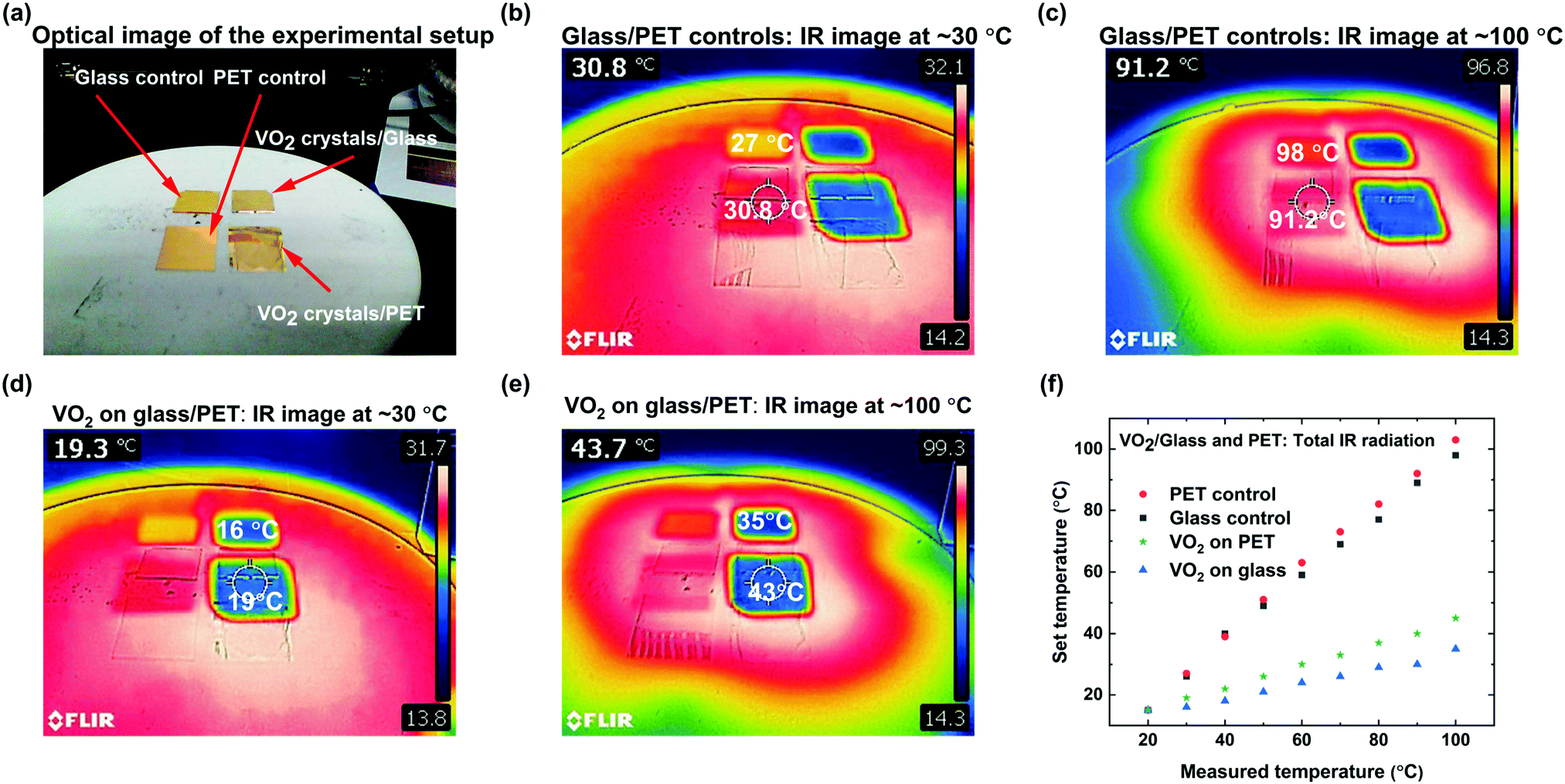 | ||
| Fig. 7 (a) Optical image of the experimental setup to measure total infrared radiation of gold coated glass and PET controls and VO2 on glass and PET (as marked). Infrared imaging of glass and PET controls at: (b) ∼30 °C and (c) ∼100 °C showing apparent temperatures of 30.8 °C and 91.2 °C respectively. Infrared imaging of gold coated VO2 microstructures on glass and PET at: (d) ∼30 °C and (e) ∼100 °C demonstrating thermal camouflage by showing apparent temperatures of 19.3 °C and 43.7 °C respectively. The colour contrast of the infrared images demonstrates the hot and cold surface with reference to one another. (f) Total radiation of VO2 microstructures drop-cast on glass and PET showing a total infrared radiation reduction capability of VO2 coated surfaces both rigid and flexible. Overall, the estimated temperature attenuation is ∼36% at 30 °C with ∼0.3%/°C reduction with rising temperatures. | ||
Conclusions
Herein a synthesis method is demonstrated that overcomes the high processing temperatures required for producing thermochromic VO2 films, and the associated limitations in the choice of substrates. Using a van der Waals substrate with inert basal planes and hydrophilic surfaces such as mica allows for the facile delamination of the synthesized oxide into aqueous colloidal suspension. The synthesis strategy allows to effectively separate the high temperature processing steps, enabling the deposition of high quality VO2 onto arbitrary substrates. TEM, EELS and XPS studies assert the high quality of the transferred VO2 crystals. The insulator-to-metal transition can be directly observed in operando during temperature-dependent high resolution TEM, leading to the observation of changes in the microcrystalline and electronic microstructures. In situ XPS findings highlighted the impact of forbidden bandgap collapse on both deep core-level spectra and valence band measurements. The optical properties of the deposited films featured excellent optical switching performance and infrared radiation attenuation. Similar optical performance was observed for flexible polyethylene terephthalate (PET) and glass substrates, featuring a change in transmission exceeding 60% at 2000 nm and adaptive thermal attenuation. This work offers the capability to readily synthesize VO2 and subsequently deposit it from solution at room temperature onto any desired substrates, including substrates that are incompatible with high temperature processing. This extends IMT applications to low-cost, flexible, but temperature sensitive platforms, expanding the scope of future VO2-based devices and applications. Furthermore, this method can likely be utilized for the synthesis of other materials that can be grown on mica to introduce colloidal heterostructures.Conflicts of interest
There are no conflicts to declare.Acknowledgements
The authors also acknowledge the facilities and technical assistance of the Micro Nano Research Facility (MNRF), the RMIT Microscopy and Microanalysis Research Facility (RMMF) and the Melbourne Centre for Nanofabrication (MCN). The authors would also like to acknowledge Billy J. Murdoch for XPS work undertaken in the RMMF.References
- N. DeForest, A. Shehabi, J. O'Donnell, G. Garcia, J. Greenblatt, E. S. Lee, S. Selkowitz and D. J. Milliron, Build. Environ., 2015, 89, 107–117 CrossRef.
- C. Sun, H. Giles and Z. Lian, Sol. Energy, 2014, 102, 1–13 CrossRef.
- R. Baetens, B. P. Jelle and A. Gustavsen, Sol. Energy Mater. Sol. Cells, 2010, 94, 87–105 CrossRef CAS.
- F. J. Morin, Phys. Rev. Lett., 1959, 3, 34 CrossRef CAS.
- In Materials Science for Solar Energy Conversion Systems, ed. C. G. Granqvist, 1991 Search PubMed.
- B. Harbecke, Appl. Phys. B, 1986, 39, 165 CrossRef.
- J. Zhou, Y. Gao, Z. Zhang, H. Luo, C. Cao, Z. Chen, L. Dai and X. Liu, Sci. Rep., 2013, 3, 3029 CrossRef.
- K. Kato, P. K. Song, H. Odaka and Y. Shigesato, Jpn. J. Appl. Phys., 2003, 42, 6523 CrossRef CAS.
- P. Jin, G. Xu, M. Tazawa and K. Yoshimura, Jpn. J. Appl. Phys., 2002, 41, L278 CrossRef CAS.
- Z. Chen, Y. Gao, L. Kang, J. Du, Z. Zhang, H. Luo, H. Miao and G. Tan, Sol. Energy Mater. Sol. Cells, 2011, 95, 2677–2684 CrossRef CAS.
- S. Wang, M. Liu, L. Kong, Y. Long, X. Jiang and A. Yu, Prog. Mater. Sci., 2016, 81, 1–54 CrossRef CAS.
- Y. Y. Luo, S. S. Pan, S. C. Xu, L. Zhong, H. Wang and G. H. Li, J. Alloys Compd., 2016, 664, 626–631 CrossRef CAS.
- R. Servin, P. Jin-Hyung, L. In-yeal, B. Jeong Min, Y. Kyung Soo and K. Gil-Ho, J. Phys. D: Appl. Phys., 2014, 47, 295101 CrossRef.
- Y. Guo, H. Xu, C. Zou, Z. Yang, B. Tong, J. Yu, Y. Zhang, L. Zhao and Y. Wang, J. Alloys Compd., 2015, 622, 913–917 CrossRef CAS.
- H. Zhang, X. Xiao, X. Lu, G. Chai, Y. Sun, Y. Zhan and G. Xu, J. Alloys Compd., 2015, 636, 106–112 CrossRef CAS.
- K. Nagashima, T. Yanagida, H. Tanaka and T. Kawai, J. Appl. Phys., 2006, 100, 063714 CrossRef.
- C. Wu, F. Feng and Y. Xie, Chem. Soc. Rev., 2013, 42, 5157–5183 RSC.
- F. Morin, Phys. Rev. Lett., 1959, 3, 34 CrossRef CAS.
- A. Cavalleri, C. Tóth, C. W. Siders, J. Squier, F. Ráksi, P. Forget and J. Kieffer, Phys. Rev. Lett., 2001, 87, 237401 CrossRef CAS.
- J. Lappalainen, S. Heinilehto, S. Saukko, V. Lantto and H. Jantunen, Sens. Actuators, A, 2008, 142, 250–255 CrossRef CAS.
- J. Zhou, Y. Gao, Z. Zhang, H. Luo, C. Cao, Z. Chen, L. Dai and X. Liu, Sci. Rep., 2013, 3, 3029 CrossRef.
- X. Chen, Q. Lv and X. Yi, Optik, 2012, 123, 1187–1189 CrossRef CAS.
- S. Babulanam, T. Eriksson, G. Niklasson and C. Granqvist, Sol. Energy Mater., 1987, 16, 347–363 CrossRef CAS.
- H. Kim, N. Charipar, E. Breckenfeld, A. Rosenberg and A. Piqué, Thin Solid Films, 2015, 596, 45–50 CrossRef CAS.
- S. K. Earl, T. D. James, T. J. Davis, J. C. McCallum, R. E. Marvel, R. F. Haglund and A. Roberts, Opt. Express, 2013, 21, 27503–27508 CrossRef.
- M. J. Dicken, K. Aydin, I. M. Pryce, L. A. Sweatlock, E. M. Boyd, S. Walavalkar, J. Ma and H. A. Atwater, Opt. Express, 2009, 17, 18330–18339 CrossRef CAS.
- J. Nag and R. Haglund Jr, J. Phys.: Condens. Matter, 2008, 20, 264016 CrossRef.
- R. Balu and P. Ashrit, Appl. Phys. Lett., 2008, 92, 021904 CrossRef.
- R. Dillon, K. Le and N. Ianno, Thin Solid Films, 2001, 398, 10–16 CrossRef.
- P. Jin, K. Yoshimura and S. Tanemura, J. Vac. Sci. Technol., A, 1997, 15, 1113–1117 CrossRef CAS.
- J. Montero, Y.-X. Ji, S.-Y. Li, G. A. Niklasson and C. G. Granqvist, J. Vac. Sci. Technol., B: Nanotechnol. Microelectron.: Mater., Process., Meas., Phenom., 2015, 33, 031805 Search PubMed.
- M. Yang, Y. Yang, B. Hong, L. Wang, K. Hu, Y. Dong, H. Xu, H. Huang, J. Zhao and H. Chen, Sci. Rep., 2016, 6, 23119 CrossRef CAS.
- Y. Nihei, Y. Sasakawa and K. Okimura, Thin Solid Films, 2008, 516, 3572–3576 CrossRef CAS.
- M. Taha, S. Walia, T. Ahmed, D. Headland, W. Withayachumnankul, S. Sriram and M. Bhaskaran, Sci. Rep., 2017, 7, 17899 CrossRef.
- T. D. Manning and I. P. Parkin, Polyhedron, 2004, 23, 3087–3095 CrossRef CAS.
- M. B. Sahana, G. N. Subbanna and S. A. Shivashankar, J. Appl. Phys., 2002, 92, 6495–6504 CrossRef CAS.
- D. Malarde, M. J. Powell, R. Quesada-Cabrera, R. L. Wilson, C. J. Carmalt, G. Sankar, I. P. Parkin and R. G. Palgrave, ACS Omega, 2017, 2, 1040–1046 CrossRef CAS.
- S. Mathur, T. Ruegamer and I. Grobelsek, Chem. Vap. Deposition, 2007, 13, 42–47 CrossRef CAS.
- X. Cao, N. Wang, J. Y. Law, S. C. J. Loo, S. Magdassi and Y. Long, Langmuir, 2014, 30, 1710–1715 CrossRef CAS.
- L. Kang, Y. Gao, Z. Zhang, J. Du, C. Cao, Z. Chen and H. Luo, J. Phys. Chem. C, 2010, 114, 1901–1911 CrossRef CAS.
- L. Kang, Y. Gao and H. Luo, ACS Appl. Mater. Interfaces, 2009, 1, 2211–2218 CrossRef CAS.
- Y. I. Tarasevich, I. G. Polyakova and V. E. Polyakov, Adsorpt. Sci. Technol., 2002, 20, 927–935 CrossRef CAS.
- U. B. Gunatilake and J. Bandara, J. Environ. Manage., 2017, 191, 96–104 CrossRef CAS.
- Y. Kanda, S. Iwasaki and K. Higashitani, J. Colloid Interface Sci., 1999, 216, 394–400 CrossRef CAS.
- J. Wang, A. G. Kalinichev and R. J. Kirkpatrick, J. Phys. Chem. C, 2009, 113, 11077–11085 CrossRef CAS.
- J. Mendialdua, R. Casanova and Y. Barbaux, J. Electron Spectrosc. Relat. Phenom., 1995, 71, 249–261 CrossRef CAS.
- T. Christmann, B. Felde, W. Niessner, D. Schalch and A. Scharmann, Thin Solid Films, 1996, 287, 134–138 CrossRef CAS.
- G. Silversmit, D. Depla, H. Poelman, G. B. Marin and R. De Gryse, J. Electron Spectrosc. Relat. Phenom., 2004, 135, 167–175 CrossRef CAS.
- J. A. Koza, Z. He, A. S. Miller and J. A. Switzer, Chem. Mater., 2011, 23, 4105–4108 CrossRef CAS.
- E. Hryha, E. Rutqvist and L. Nyborg, Surf. Interface Anal., 2012, 44, 1022–1025 CrossRef CAS.
- M. J. Powell, I. J. Godfrey, R. Quesada-Cabrera, D. Malarde, D. Teixeira, H. Emerich, R. G. Palgrave, C. J. Carmalt, I. P. Parkin and G. Sankar, J. Phys. Chem. C, 2017, 121, 20345–20352 CrossRef CAS.
- S. A. Bukhari, S. Kumar, P. Kumar, S. P. Gumfekar, H.-J. Chung, T. Thundat and A. Goswami, Appl. Surf. Sci., 2020, 146995, DOI:10.1016/j.apsusc.2020.146995.
- Q. Song, W. Gong, G. Ning, H. Mehdi, G. Zhang, J. Ye and Y. Lin, Phys. Chem. Chem. Phys., 2014, 16, 8783–8786 RSC.
- F. Gracia, F. Yubero, J. Espinos and A. Gonzalez-Elipe, Appl. Surf. Sci., 2005, 252, 189–195 CrossRef CAS.
- Y. Yang, H. Tu, A. Zhang, D. Du and Y. Lin, J. Mater. Chem., 2012, 22, 4977–4981 RSC.
- Y. Luo, L. Zhu, Y. Zhang, S. Pan, S. Xu, M. Liu and G. Li, J. Appl. Phys., 2013, 113, 183520 CrossRef.
- R. M. Öksüzoğlu, P. Bilgiç, M. Yıldırım and O. Deniz, Opt. Laser Technol., 2013, 48, 102–109 CrossRef.
- S. Beke, S. Giorgio, L. Kőrösi, L. Nanai and W. Marine, Thin Solid Films, 2008, 516, 4659–4664 CrossRef CAS.
- E. M. Heckman, L. P. Gonzalez, S. Guha, J. O. Barnes and A. Carpenter, Thin Solid Films, 2009, 518, 265–268 CrossRef CAS.
- A. Cavalleri, M. Rini, H. Chong, S. Fourmaux, T. Glover, P. Heimann, J. Kieffer and R. Schoenlein, Phys. Rev. Lett., 2005, 95, 067405 CrossRef CAS.
- Y. Goltvyanskyi, I. Khatsevych, A. Kuchuk, V. Kladko, V. Melnik, P. Lytvyn, V. Nikirin and B. Romanyuk, Thin Solid Films, 2014, 564, 179–185 CrossRef CAS.
- M. Wan, M. Xiong, N. Li, B. Liu, S. Wang, W.-Y. Ching and X. Zhao, Appl. Surf. Sci., 2017, 410, 363–372 CrossRef CAS.
- C. Ramana, O. Hussain, B. S. Naidu and P. Reddy, Thin Solid Films, 1997, 305, 219–226 CrossRef CAS.
- H. Wu, Q. Fu and X. Bao, J. Phys.: Condens. Matter, 2016, 28, 434003 CrossRef.
- P. Schilbe, Phys. B, 2002, 316, 600–602 CrossRef.
- D. Bhardwaj, A. Goswami and A. Umarji, J. Appl. Phys., 2018, 124, 135301 CrossRef.
- S. Xie, E. Iglesia and A. T. Bell, Langmuir, 2000, 16, 7162–7167 CrossRef CAS.
- A. Akande, Microwave synthesis of vanadium oxide (VOx) nanoparticles and their application in methane sensing, 2014.
- G. Bodurov, T. Ivanova, M. Abrashev, Z. Nenova and K. Gesheva, Phys. Procedia, 2013, 46, 127–136 CrossRef CAS.
- H.-T. Kim, B.-G. Chae, D.-H. Youn, G. Kim, K.-Y. Kang, S.-J. Lee, K. Kim and Y.-S. Lim, Appl. Phys. Lett., 2005, 86, 242101 CrossRef.
- X. Wang, H. Li, Y. Fei, X. Wang, Y. Xiong, Y. Nie and K. Feng, Appl. Surf. Sci., 2001, 177, 8–14 CrossRef CAS.
- K. Okimura, N. Hanis Azhan, T. Hajiri, S.-I. Kimura, M. Zaghrioui and J. Sakai, J. Appl. Phys., 2014, 115, 153501 CrossRef.
- M. Pan, J. Liu, H. Zhong, S. Wang, Z.-F. Li, X. Chen and W. Lu, J. Cryst. Growth, 2004, 268, 178–183 CrossRef CAS.
- F. Ureña-Begara, A. Crunteanu and J.-P. Raskin, Appl. Surf. Sci., 2017, 403, 717–727 CrossRef.
- B. Hu, Y. Ding, W. Chen, D. Kulkarni, Y. Shen, V. V. Tsukruk and Z. L. Wang, Adv. Mater., 2010, 22, 5134–5139 CrossRef CAS.
- Y. Zhang, H. Jia, R. Wang, C. Chen, X. Luo, D. Yu and C. Lee, Appl. Phys. Lett., 2003, 83, 4631–4633 CrossRef CAS.
- H. Mo, G. Wang, F. Liu and P. Jiang, RSC Adv., 2016, 6, 83163–83174 RSC.
- R. Lopez, L. Boatner, T. Haynes, L. C. Feldman and R. Haglund Jr, J. Appl. Phys., 2002, 92, 4031–4036 CrossRef CAS.
- D. Kim and H. Kwok, Appl. Phys. Lett., 1994, 65, 3188–3190 CrossRef CAS.
- X. Wu, Y. Tao, L. Dong, Z. Wang and Z. Hu, Mater. Res. Bull., 2005, 40, 315–321 CrossRef CAS.
- C. C. Kwan, C. Griffiths and H. Eastwood, Appl. Phys. Lett., 1972, 20, 93–95 CrossRef CAS.
- M. F. Jager, C. Ott, P. M. Kraus, C. J. Kaplan, W. Pouse, R. E. Marvel, R. F. Haglund, D. M. Neumark and S. R. Leone, Proc. Natl. Acad. Sci. U. S. A., 2017, 114, 9558–9563 CrossRef CAS.
- F. Béteille, L. Mazerolles and J. Livage, Mater. Res. Bull., 1999, 34, 2177–2184 CrossRef.
- Y. Jo, M. Kim and B. Kim, Nanotechnology, 2016, 27, 435704 CrossRef.
- M. R. Bayati, R. Molaei, F. Wu, J. D. Budai, Y. Liu, R. J. Narayan and J. Narayan, Acta Mater., 2013, 61, 7805–7815 CrossRef CAS.
- R. McGee, A. Goswami, S. Pal, K. Schofield, S. A. M. Bukhari and T. Thundat, Phys. Rev. Mater., 2018, 2, 034605 CrossRef CAS.
- Y. Wang, Z. Zhang, Y. Zhu, Z. Li, R. Vajtai, L. Ci and P. M. Ajayan, ACS Nano, 2008, 2, 1492–1496 CrossRef CAS.
- T. E. Alivio, D. G. Sellers, H. Asayesh-Ardakani, E. J. Braham, G. A. Horrocks, K. E. Pelcher, R. Villareal, L. Zuin, P. J. Shamberger and R. Arróyave, Chem. Mater., 2017, 29, 5401–5412 CrossRef CAS.
- N. F. Quackenbush, H. Paik, M. E. Holtz, M. J. Wahila, J. A. Moyer, S. Barthel, T. O. Wehling, D. A. Arena, J. C. Woicik and D. A. Muller, Phys. Rev. B, 2017, 96, 081103 CrossRef.
- R. Mossanek and M. Abbate, J. Phys.: Condens. Matter, 2007, 19, 346225 CrossRef.
- H. Abe, M. Terauchi, M. Tanaka, S. Shin and Y. Ueda, Jpn. J. Appl. Phys., 1997, 36, 165 CrossRef CAS.
- Z. Shao, X. Cao, H. Luo and P. Jin, NPG Asia Mater., 2018, 10, 581 CrossRef.
- C. Blaauw, F. Leenhouts, F. van der Woude and G. Sawatzky, J. Phys. C: Solid State Phys., 1975, 8, 459 CrossRef CAS.
- A. Bianconi, Phys. Rev. B: Condens. Matter Mater. Phys., 1982, 26, 2741 CrossRef CAS.
- V. Klimov, I. Timofeeva, S. Khanin, E. Shadrin, A. Ilinskii and F. Silva-Andrade, Tech. Phys., 2002, 47, 1134–1139 CrossRef CAS.
- G. Xu, P. Jin, M. Tazawa and K. Yoshimura, Jpn. J. Appl. Phys., 2004, 43, 186 CrossRef CAS.
Footnote |
| † Electronic supplementary information (ESI) available. See DOI: 10.1039/d0ma00338g |
| This journal is © The Royal Society of Chemistry 2020 |