
 Open Access Article
 This Open Access Article is licensed under a Creative Commons Attribution-Non Commercial 3.0 Unported Licence
Hierarchical core–shell heterostructure of H2O-oxidized ZnO nanorod@Mg-doped ZnO nanoparticle for solar cell applications
Christian Mark
Pelicano
 *a,
Itaru
Raifuku
a,
Yasuaki
Ishikawa
b,
Yukiharu
Uraoka
b and
Hisao
Yanagi
b
*a,
Itaru
Raifuku
a,
Yasuaki
Ishikawa
b,
Yukiharu
Uraoka
b and
Hisao
Yanagi
b
aGraduate School of Materials Science, Nara Institute of Science and Technology Takayama, 8916-5, Ikoma City, Nara 630-0192, Japan. E-mail: christian.pelicano.ce0@ms.naist.jp
bGraduate School of Science and Technology, Nara Institute of Science and Technology Takayama, 8916-5, Ikoma City, Nara 630-0192, Japan
First published on 1st July 2020
Abstract
Herein, a core–shell heterostructure of H2O-oxidized ZnO nanorod (NR)@Mg-doped ZnO (MZO) nanoparticles (NP) with superior charge transfer capabilities is presented for the first time. ZnO NRs were strategically designed using a low-temperature and sustainable H2O oxidation technique and followed by low-temperature annealing of a spin-coated MZO precursor to form a core–shell heterostructure. Surface morphological and nanobeam electron diffraction (NBD) analysis validated the high-quality crystalline nature of the core–shell heterostructure. The verification of Mg dopant inclusion in the ZnO lattice and uniform distribution were established from X-ray (XRD, XPS, EDX), Raman and electron energy-loss (EELS) spectroscopy analyses. The ZnO NR@MZO NP core–shell film preserved the excellent transparency of the original ZnO NRs and displayed the highest conductivity due to the increased carrier concentration in the MZO shell. Steady-state photoluminescence (PL) intensity of the perovskite film on top of the ZnO NR@MZO NP core–shell film showed the strongest quenching among the samples indicating the fastest electron transfer. This ZnO NR@MZO NP core–shell heterostructure could provide a more efficient transmission channel by supplying a larger electronic contact with the light absorber layer and a direct path for electron transport to the cathode. Ultimately, our results highlight the great potential of the ZnO NR@MZO NP core–shell structure as an electrode not only for photovoltaics but also in other future flexible optoelectronic devices.
1. Introduction
Zinc oxide (ZnO) is a multifunctional semiconductor that has attracted extensive interest over the past decades due to its unique chemical, optical and electrical properties.1 It is an n-type II–IV semiconductor possessing a wide band gap (3.37 eV) and large exciton binding energy (60 meV).2 These valuable properties make ZnO an excellent candidate for optoelectronic applications including solar cells,3–7 transparent conducting oxides (TCO),8–10 light emitting diodes (LEDs),11–13 ultraviolet (UV) lasers,14,15 and photodetectors.16,17 More specifically for solar cells, nanostructured ZnO can serve as an electron-transporting layer (ETL) or transparent conductive electrode (TCO) owing to its inherent high electron mobility and high conductivity.18–20 In fact, nanostructured ZnO has more flexibility in synthesis methods and morphologies compared with TiO2. Recently, various one-dimensional (1D) ZnO nanostructures (NSs) including nanowires (NWs), nanorods (NRs) and nanotubes (NTs) have been developed to drastically boost the charge transport and accelerate the collection of photogenerated electrons.21–24 This architecture provides a direct conduction pathway and is expected to lessen interparticle hops, which is the main issue for films based on nanoparticles (NPs). However, solar cell performance is usually restricted by inadequate surface area of these 1D NSs due to poor electronic contact with the absorber layer. Thus, the geometrical structure of the ETL films plays a significant role in enhancing charge transport.One of the approaches to increase electronic contact and at the same time improve charge transport is through the deposition of a wider band gap nanomaterial onto the 1D ZnO NS surface, creating a core–shell heterostructure.25,26 A more efficient electron extraction and limited charge recombination can be expected from this system due to the higher electron mobility and the additional surface area of the wider band gap nanostructured shell. A number of studies have reported heterostructures based on ZnO NRs. For example, Zhong et al. fabricated a ZnO@TiO2 NR core–shell arrays-based perovskite solar cell (PSC) with improved performance compared to ZnO NR-based PSC.27 The ZnO NRs were synthesized using a complex modified polymer soft template method followed by deposition of TiO2 NPs via hydrolysis and polycondensation reaction. Another study used the ZnO NWs@Al-doped ZnO (AZO) thin film core–shell structure as a photoanode to enhance the performance of CdS quantum dot sensitized solar cells.28 The core–shell structure was obtained using chemical bath deposition and subsequently, thermal oxidation of the AZO precursor at a high temperature of 450 °C. Hence, it is necessary to develop a simpler, faster and energy-efficient protocol for producing ZnO-based core–shell heterostructures.
Herein, we introduce a core–shell heterostructure of H2O-oxidized ZnO NRs@Mg-doped ZnO (MZO) NPs with enhanced charge transporting capabilities. The ZnO NRs were grown using our original H2O oxidation technique (T ≤ 100 °C), which uses only pure water to transform a vacuum-deposited Zn thin film into a NR-based ZnO film. H2O oxidation process avoids the use of toxic chemical reagents, elevated temperature and complex equipment for preparing ZnO nanomaterials.29,30 Subsequently, a facile spin-coating and low temperature annealing process is used to assemble MZO NPs onto the ZnO NR surface. The properties of the core–shell structure were examined through comprehensive structural, optical, chemical and electrical characterizations. A proposed electron transport mechanism was also given to clearly present the advantage of the heterostructure system. To the best of the authors’ knowledge, this study is the first to report a core–shell heterostructure composed of a ZnO NR core with doped ZnO NP as its shell. Based on our results, this low-temperature processed NR@MZO NP core–shell structure can pave the way for future flexible and highly efficient photovoltaics.
2. Experimental
2.1 Fabrication of H2O-oxidized ZnO NRs@Mg-doped ZnO NPs core–shell heterostructure
ITO-glass substrates (Luminescence Tech. Corp.) were etched with diluted hydrochloric acid and cleaned via sonication with detergent, ultrapure water, acetone and methanol for 15 min, separately. Then, the substrates were treated with UV/O3 for 10 min to remove organic impurities. Before depositing Zn thin films, a 0.50 M zinc acetate (Zn(CH3COO)2, Wako) in methanol![[thin space (1/6-em)]](https://www.rsc.org/images/entities/char_2009.gif) :water (10:1) solution was spin-coated onto the substrates at 5000 rpm for 30 s. The films were dried first at 100 °C for 15 min and then annealed at 200 °C for 1 h to form a compact ZnO seed layer. Zn thin films were then thermally evaporated on top of the ZnO seed layer at a base pressure of 4 × 10⁻⁴ Pa. The Zn thin films were subsequently immersed in ultrapure water at 90 °C for 8 h to obtain ZnO NRs. To assemble MZO NPs over the surface of ZnO NRs, a certain amount of Mg(CH3COO)2·4H2O was added in the Zn(CH3COO)2·2H2O in methanol:water (10:1) solution to prepare an MZO precursor solution with a nominal molar ratio (Mg/(Mg + Zn)) of 0 and 10%. Afterwards, the MZO precursor was spin-coated on top of H2O-oxidized ZnO NRs at 4000 rpm for 30 s and annealed at 200 °C for 1 h.
:water (10:1) solution was spin-coated onto the substrates at 5000 rpm for 30 s. The films were dried first at 100 °C for 15 min and then annealed at 200 °C for 1 h to form a compact ZnO seed layer. Zn thin films were then thermally evaporated on top of the ZnO seed layer at a base pressure of 4 × 10⁻⁴ Pa. The Zn thin films were subsequently immersed in ultrapure water at 90 °C for 8 h to obtain ZnO NRs. To assemble MZO NPs over the surface of ZnO NRs, a certain amount of Mg(CH3COO)2·4H2O was added in the Zn(CH3COO)2·2H2O in methanol:water (10:1) solution to prepare an MZO precursor solution with a nominal molar ratio (Mg/(Mg + Zn)) of 0 and 10%. Afterwards, the MZO precursor was spin-coated on top of H2O-oxidized ZnO NRs at 4000 rpm for 30 s and annealed at 200 °C for 1 h.
2.2 Materials characterization
A low vacuum scanning electron microscope (SEM, Hitachi SU6600) equipped with an energy-dispersive X-ray spectroscopy (EDX) system was used to observe the surface morphologies and acquire the EDX data of the samples. High-resolution transmission electron microscopy (TEM) images, nanobeam electron diffraction (NBD) pattern, and electron energy loss spectroscopy (EELS) elemental mappings were obtained using JEOL JEM-3100FEF operating at 300 kV. The sample for TEM measurement was prepared by dry adhesion of the nanostructures on a Cu grid. The crystallinity and phase composition of the samples were studied using a Rigaku X-ray diffractometer (XRD, RINT-TTR III) with CuKα radiation (λ = 1.5418 Å). Raman scattering measurement was performed at room temperature using a Raman spectrometer (JASCO NRS-4100). The optical transmission and absorption spectra of the films were measured using a UV-Vis spectrophotometer (JASCO V-530). PL spectra were obtained under ultraviolet excitation (λex = 365 nm) using a high-pressure mercury-vapour light source (Olympus BH2-RFL-T3) coupled with a microscope (Olympus BX51) and a CCD spectrometer (Hamamatsu PMA-12). The surface chemistry of the films was further investigated by X-ray photoelectron spectroscopy (XPS, PHI5000 VersaProbeII, ULVAC-PHI) at room temperature with Al-Kα radiation (1486.6 eV). Charging effects on the binding energies were calibrated with respect to the C 1s peak (284.6 eV). Current–voltage (I–V) curves for conductivity measurement were recorded using a Keithley 2611B System Source Meter unit (Bunko-keiki, CEP-2000RP). The perovskite films used for steady-state PL and absorbance measurements were deposited on top of the ETL films using fast deposition crystallization.29 The perovskite precursor solution (45 wt%) was prepared by mixing equal molar amounts of (1.2 mmol) PbI2 (99.999%, Wako) and of CH3NH3I (98.0%, Wako) in 1 mL of anhydrous N,N-dimethylformamide (DMF, Wako). 60 μL of perovskite precursor solution was then spin coated onto the substrates for 30 s. The substrates were spun at 5000 rpm and after 4–6 seconds, 150 μL of toluene was quickly dropped onto the center of the substrate, followed by thermal annealing at 70 °C for 10 min.3. Results and discussion
In general, surface engineering of a core structure with NP is a great strategy to provide additional surface area and improve the charge transfer between interfaces. For clarity, the undoped core–shell sample is denoted here as NR@NP whereas the doped counterpart is NR@MZO NP. The innovative route for preparing a hierarchical core–shell structure of H2O-oxidized ZnO NR@MZO NP involved two key steps, as shown in Fig. 1. | ||
| Fig. 1 Schematic illustration for preparing the hierarchical core–shell structure of ZnO NR@MZO NPs. | ||
Firstly, a 100 nm-thick Zn thin film was deposited onto a compact ZnO layer/ITO-glass substrate via thermal evaporation. Subsequently, the samples underwent H2O oxidation by immersing them inside a beaker filled with ultrapure H2O and heated at 90 °C for 8 h using a hotplate. Fig. 2 shows the SEM images and the corresponding EDX measurements of the H2O-oxdized ZnO NRs and NR@MZO NP core–shell array. Clustered ZnO NRs are seen to evolve from the Zn thin film, as shown in Fig. 2(a). More specifically, the ZnO NRs are tilted from the vertical direction. The shape of the NRs is cuboid with rounded tips and smooth outer surface. The overall nanostructured ZnO film generated has an average thickness of ∼250 nm and each individual NR has a diameter ranging from 70–90 nm. The oxidation of the Zn thin film to create ZnO can be described by the following electrochemical reactions:
 | ||
| Fig. 2 SEM images of (a) ZnO NRs formed after H2O oxidation at 90 °C for 8 h, (b) NR@NP, and (c) NR@MZO NP core–shell samples. | ||
(A) Dissolution of Zn (redox reaction):
| (Anode) Zn(S) → Zn(aq)2+ + 2e− | (1) |
| (cathode) 2H2O(l) + 2e− → H2(g) + 2OH− | (2) |
 | (3) |
(B) Formation of ZnO:
| Zn(aq)2+ + 2OH(aq)− → ZnO + H2O | (4) |
Initially, the anodic corrosion of Zn triggers the release of 2 electrons (eqn (1)) in H2O. Simultaneously, these electrons will be consumed in the reduction of H2O and dissolved oxygen to produce OH− ions (eqn (2) and (3)). These OH− ions then react with Zn2+ ions to generate ZnO crystals through hydrolysis (eqn (4)). The evolution of gas bubbles during the early stage of Zn thin film oxidation verifies the production of H2 gas. Additionally, the growth mechanism of ZnO crystals into NRs could be linked to the well-established reconstruction of high-surface energy polar planes of wurtzite ZnO. The negatively charged O2− terminated (00![[1 with combining macron]](https://www.rsc.org/images/entities/char_0031_0304.gif) ) planes of the existing ZnO molecules in H2O strategically adsorb onto the Zn2+ terminated (001) planes of the preformed ZnO layers, steering the development of one-dimensional (1D) ZnO NRs.29
) planes of the existing ZnO molecules in H2O strategically adsorb onto the Zn2+ terminated (001) planes of the preformed ZnO layers, steering the development of one-dimensional (1D) ZnO NRs.29
The resulting ZnO NRs are then modified via a facile spin-coating of a methanolic solution of Mg(CH3COO)2·4H2O and Zn(CH3COO)2·2H2O with a nominal molar ratio of 0% and 10% (Mg/(Mg + Zn)). After that, the resulting films were annealed at 200 °C for 1 h in ambient air to finally form the NR@NP core–shell structure. It can be seen that the NR morphology has no considerable change when NRs were covered with NPs, as shown in Fig. 2(b). The ZnO NPs having an average diameter of 5–10 nm developed uniformly and filled the interstices of the NRs. Fig. 2(c) shows that the NRs decorated with MZO NPs have a very similar hierarchical core–shell structure as with the undoped counterpart. Meanwhile, the MZO NPs now have a better coverage of NRs by filling up the spaces in between the NRs. The chemical compositions of all the samples were examined using EDX analyses, as illustrated in Fig. 2. The undoped samples only revealed Zn and O elements implying the high-purity of the samples. The EDX spectrum of the NR@MZO NP sample demonstrates the presence of Zn, O and Mg elements (1.23 at%), suggesting that the NPs were successfully doped with Mg.
The influence of interfacial modification on the phase composition and crystallinity of ZnO NRs is investigated through X-ray diffraction (XRD) analysis, as shown in Fig. 3(a). It is found that all diffraction peaks can be indexed to the hexagonal wurtzite ZnO crystal structure (JCPDS No. 36-1451), except for the peaks (marked with a circle) from the ITO/glass substrate. All the patterns exhibited sharp and strong ZnO peaks confirming that all the samples are highly crystalline. It should be noted that the intensity of the (101) peak of the NR sample is stronger than its (002) peak verifying the tilted nature of H2O-oxidized ZnO NRs. The NR@MZO NP sample displayed identical diffraction peaks to those of pure NR@NP signifying the absence of second phase formation, such as MgO or other impurities, after annealing at 200 °C. This finding is in agreement with the study reported by Bian et al., wherein a higher calcination temperature of 400 °C is needed for the complete conversion of anhydrous Mg acetate to MgO.31 Moreover, the (002) peak for the NR@MZO NP shifted slightly towards higher θ values in comparison to the NR@NP, as shown in the inset of Fig. 3(a). This is possibly due to lattice disorder and strain induced by the introduction of Mg dopants into the Zn2+ sites.32 The calculated lattice constant “a” for all the samples did not show any significant change, whereas the lattice constant “c” decreased from 5.1126 Å in NR@NP to 5.1056 Å in the NR@MZO NP core–shell sample. Based on Vegard's law, this observed c-axis shrinkage is highly probable for a Mg-substituted ZnO solid solution due to the smaller ionic radius of Mg2+ (0.57 Å) than that of Zn2+ (0.60 Å).33
 | ||
| Fig. 3 (a) XRD patterns and (b) Raman spectra of ZnO NR, NR@NP, and NR@MZO NP. | ||
In order to explore in detail the hierarchical structure at the nanoscale, TEM and EELS elemental mapping analyses were carried out, as shown in Fig. 4. The TEM and HRTEM images show an individual ZnO NR uniformly decorated with MZO NPs across its outer surface confirming the formation of a core–shell NR structure and supporting the SEM results. Furthermore, the HRTEM image of a single MZO NP visibly attached on the NR surface shows a lattice spacing of 0.255 nm corresponding to the distance between the (002) plane of wurtzite ZnO. As expected, the corresponding nanobeam electron diffraction (NBD) pattern presents a concentric ring pattern which implies the polycrystalline nature of the NR@MZO NP core–shell structure. The EELS elemental mapping images of Mg, Zn, and O elements based on the TEM image, are shown in Fig. 4(d)–(f), respectively. Other than the dense Zn and O elements, a relatively lower density of Mg element can be seen throughout the entire surface area of the NR, signifying the uniform distribution of Mg dopant atoms.
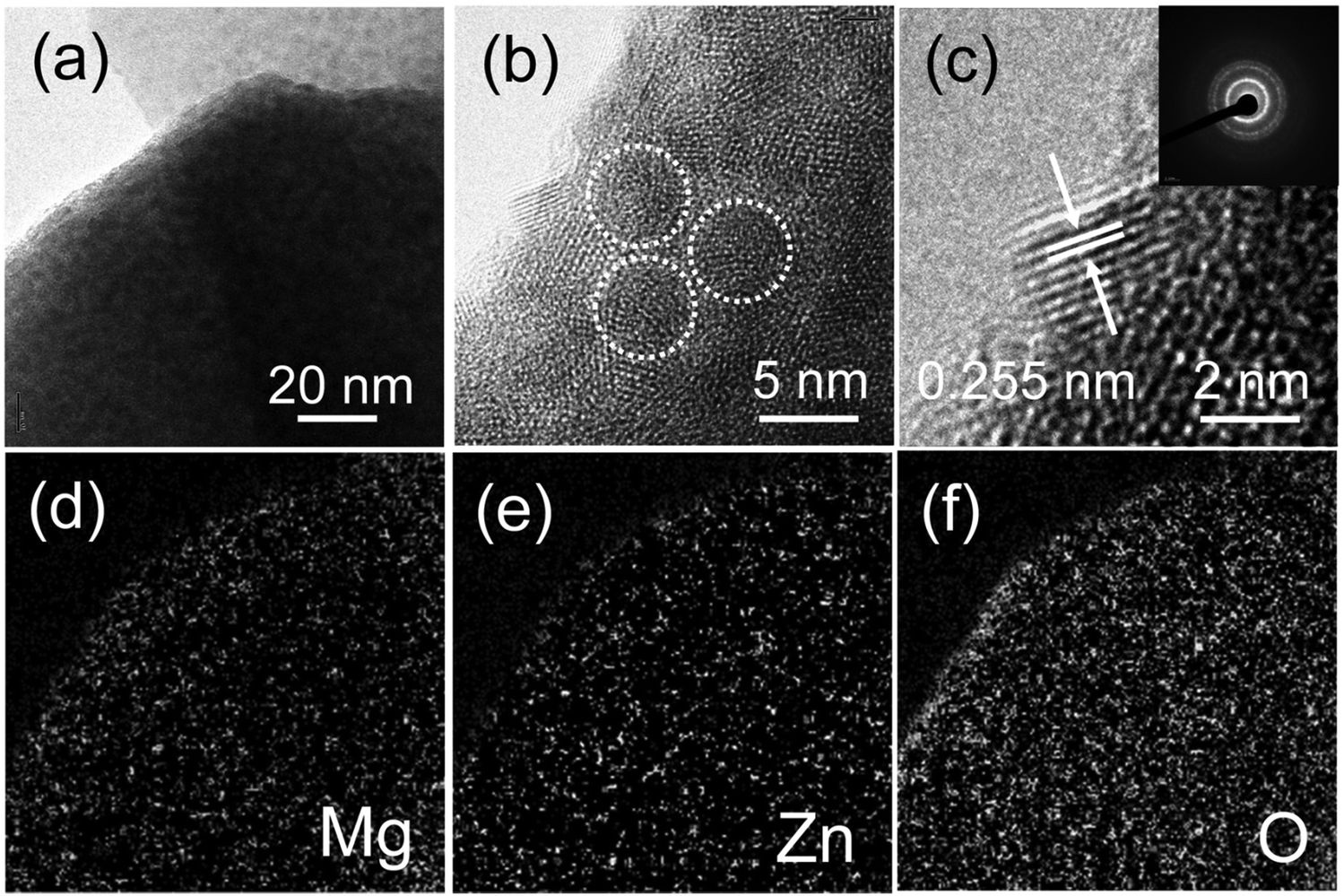 | ||
| Fig. 4 (a) TEM and (b), (c) HRTEM images of a single ZnO NR decorated with MZO NPs (inset: nanobeam electron diffraction pattern). Images (d)–(f) are its corresponding EELS elemental mapping. | ||
Raman spectroscopy was implemented to study the vibrational properties of the core–shell NR structure. According to group theory, wurtzite ZnO belongs to the space group C6v4 with two formula units per primitive cell. The Raman-active phonon modes include E(low)2, E(high)2 and E1 longitudinal optical (LO) mode, among others.34Fig. 3(b) shows the representative Raman spectra collected at room temperature for all the samples under the excitation of a 532 nm laser beam over the spectral range of 70–590 cm−1. All the films exhibited identical characteristic Raman modes linked with wurtzite ZnO. The two dominant peaks detected at ∼99.5 and ∼437 cm−1 are attributed to the low and high E2 modes of nonpolar optical phonons, respectively.34 These intense modes further affirmed the highly-crystalline nature of the samples. The broad and suppressed peak at ∼570 cm−1 corresponds to the E(LO)2 mode, which is possibly associated to the structural defects owing to interstitial oxygen vacancies.35 In addition, broader scattering modes for the NR@MZO NP core–shell sample can be evidently seen, which further confirms the stress formation arising from Mg dopant inclusion in the ZnO lattice.
To understand the changes in the chemical binding environment of the surface atoms of the NR@MZO NP core–shell structure, the core levels of Zn 2p, O 1s and Mg 2p states were examined using X-ray photoelectron spectroscopy (XPS) measurements, as depicted in Fig. 5. Only Zn, O, C and Mg-related core levels are detected in the survey spectra (Fig. 5(a)). The C 1s signal at 284.6 eV can be assigned to adventitious carbon and the charge shifted spectra were corrected using this peak as a reference. Fig. 5(b) shows the high-resolution Zn 2p spectrum of ZnO NRs displaying two peaks of Zn 2p3/2 (1020.6 eV) and Zn 2p1/2 (1043.6 eV) with a splitting energy of 23.0 eV, specifying that the Zn element exists in the form of Zn2+.36 Apparently, Zn 2p3/2 (1021.5 eV) and Zn 2p1/2 (1044.6 eV) peaks shifted towards higher binding energies after wrapping undoped ZnO NPs on the NRs. One possible reason for this shift is the production of Zn(OH)2 from the incomplete conversion of Zn precursor to ZnO due to the low annealing temperature applied.37 Interestingly, the binding energies of Zn 2p3/2 (1021 eV) and Zn 2p1/2 (1044 eV) peaks of the NR@MZO NP core–shell sample are lower than the NR@NP core–shell but higher than ZnO NRs. This suggests that an energy transfer between Zn2+ ions and substitutional Mg2+ ions has occurred and at the same time reduced the concentration of the OH− group.38 This can be further established by checking the O 1s spectra of the films.
 | ||
| Fig. 5 (a) XPS survey spectra and high-resolution XPS spectra of (b) Zn 2p, (c) O 1s and (d) Mg 2p of ZnO NRs modified with MZO NPs. | ||
From Fig. 5(c), it can be observed that the O 1s spectra were asymmetric; therefore, each spectrum was divided into three peaks located at 530.3 eV, 531.0 eV and 531.9 eV. The OL peak at 530.3 eV corresponds to O2− ions on the wurtzite structure of the Zn2+ ion array, which are either bonded with Zn or substitutional Mg atoms.39 The OV peak centered at 531.0 eV is usually assigned to O2− in oxygen-deficient sites within the ZnO matrix which is indicative of the corresponding oxygen vacancy concentration.40 The OC peak located at 531.9 eV is ascribed to some chemisorbed oxygen components in the form of H2O, –CO3 and OH− groups.41 Notice that the O 1s spectrum of the NR@NP core–shell film also shifted towards higher binding energies owing to the emergence of a hydrated layer on the ZnO surface. On the other hand, the incorporation of Mg dopant into the ZnO lattice shifted the O 1s spectrum by around 0.5 eV to lower binding energies and apparently caused it to become broader. This means that Mg doping initiated an additional Zn–O–Mg bonding. Most importantly, the existing Zn2+ ions in the crystal lattice can now attract more electrons due to its larger electronegativity (1.65) than Mg (1.31).42 Accordingly, the electron density on the Zn–O bonds increases and causes a shift in the O 1s peak towards lower binding energies. Simultaneously, this phenomenon results in an increase in oxygen vacancies, which is the reason behind the broadening of the O 1s peak. The high-resolution Mg 2p spectrum of the NR@MZO NP core–shell film shows the presence of an Mg 2p3/2 peak positioned at 49.4 eV. This peak both validates that Mg doping has successfully taken place in the ZnO host and MgO (Mg 2p3/2: 51 eV) is not present on the surface of the NR@MZO NP core–shell structure.43
An electron-transporting layer should be transparent enough to allow a significant amount of light to be transmitted to the active layer, which generates charge carriers; hence, the optical transmission spectra of the films were measured using a UV-vis spectrometer, as shown in Fig. 6(a). All the films are found to be highly transparent with an average transmittance of about 80% for wavelengths higher than 500 nm. The small difference in transparency among the samples denotes that this property is insensitive to the presence of a NP shell and Mg dopant. Fig. 6(b) shows the room temperature PL spectra of ZnO NRs and NR@NP core–shell samples under an excitation wavelength of 365 nm. It can be observed that the PL spectra of both undoped and doped NR@NP core–shell films feature a parallel set of key spectral components. First, the blue emission band centred around 450 nm (2.75 eV) which is usually assigned to the transition from extended interstitial Zn (Zni) states to the valence band.44 The extended Zni states typically include localized Zni states, Zni2+ and complex defects having energetic locations deep in the band gap depending on the synthesis approach used.45 Furthermore, the orange-red visible emission band centered at 620 nm (2.0 eV) is caused by transition from the Zni to the oxygen interstitial (Oi) states, which normally occurs for oxygen-rich structures.46 It is also evident that the intensity of the visible bands increased for the NR@NP core–shell samples. This could be due to the large surface area of the NP shell and higher concentration of ZnO on the samples. In order to establish the effect of assembling a NR@MZO NP core–shell structure on the conductivity of the ZnO NR film, the devices composed of ITO/ZnO NR or NR@NP or NR@MZO NP/Ag are fabricated, and the I–V characteristics are shown in Fig. 7(a). Clearly, a decrease in the conductivity has taken place when ZnO NPs were deposited on the NR surface. Again, this could be linked to the presence of Zn(OH)2 on the NR@NR core–shell sample. In contrast, the device based on a NR@MZO NP core–shell exhibited the highest conductivity among the samples, which can be explained in terms of the increased carrier concentration through Mg doping.47 As stated earlier, the NR@MZO NP core–shell film revealed a higher amount of oxygen vacancies and this increase in carrier concentration led to a higher conductivity for the doped core–shell sample.
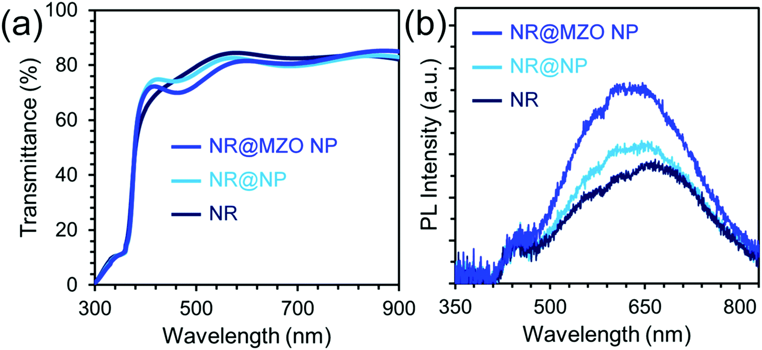 | ||
| Fig. 6 (a) Optical transmission and (b) room temperature PL spectra of ZnO NR, NR@NP, and NR@MZO NP. | ||
 | ||
| Fig. 7 (a) I–V characteristics of the electron-only devices based on ZnO NRs and ZnO NRs@MZO NPs. (b) Steady-state PL and (c) absorption spectra of CH3NH3PbI3 films on top of ZnO NRs and ZnO NRs@MZO NPs. | ||
To unravel the charge dynamics and applicability of the NR@MZO NP core–shell structure as an electron-transporting layer (ETL) for solar cells, the steady-state PL spectra of the CH3NH3PbI3 layer as an active layer on top of all the films were investigated, as shown in Fig. 7(b). It has been reported that the variation in PL intensity of perovskite hints at the variation in the local non-radiative decay rate.48 The peak at around 770 nm is related to the intrinsic fluorescence emission of the CH3NH3PbI3 layer (purple line). Compared with ZnO NR ETL, the PL intensity of the ITO/NR@NP/perovskite film (light blue line) was reduced by half indicating that more electrons were transmitted from the perovskite to the NR@NP core–shell film. Even in the presence of Zn(OH)2 species on its surface, the additional surface area brought by the NP shell created a larger electronic contact with the active layer, bringing more electrons to be transported and suppressing charge recombination. Then, for the perovskite film with the NR@MZO NP core–shell as ETL (dark blue line), the PL intensity was further quenched by 50% than that of the NR film. This means that the NR@MZO NP core–shell structure offers the fastest electronic extraction and transportation capability. This behaviour of the NR@MZO NP film could be associated to the increased carrier concentration via Mg doping as stated earlier. In turn, this increase in carrier density could raise the Fermi level into the conduction band of ZnO. Consequently, the resulting band alignment of MZO NPs with the active layer makes the extraction of electrons much easier.47 Moreover, while the ZnO NRs allow the electrons to have a direct path to the cathode, the MZO NPs provide a more efficient layer as a transmission channel to the NRs, as shown in Fig. 8. For those reasons, solar cell devices can be expected to achieve superior performances based on this ETL. Fig. 7(c) presents the absorption spectra of perovskite films on top of the different ETL nanostructured films. Obviously, the NR@NP core–shell structured samples displayed higher absorption of light in comparison to ZnO NRs alone, which agrees well with the PL analysis. These results highlight the applicability of our NR@MZO NP core–shell film as an alternative electron-transporting layer not only for photovoltaics but also for other future flexible optoelectronic devices.
 | ||
| Fig. 8 Electron transportation mechanism of the ZnO NR@MZO NP core–shell structure, in which both ZnO NRs and MZO NPs provide channels for electron transport. | ||
4. Conclusion
In summary, we developed a hierarchical core–shell structure of H2O-oxidized ZnO NR@MZO NPs and presented its electron-transporting properties. A facile spin-coating and low-temperature annealing process of the MZO precursor caused the growth of NPs on the NR surface, creating a core–shell structure. SEM and HRTEM/NBD images confirmed that the core–shell structure has a high-quality crystalline nature. XPS, EDX, and Raman analyses proved the successful replacement of Zn2+ by Mg2+ ions in the ZnO lattice. Compression of lattice constant “c” was also detected from XRD, which further verified the formation of an Mg-substituted ZnO solution. In addition, EELS elemental mapping established uniform Mg dopant distribution across the surface of the NRs. The core–shell samples retained the high transparency of the original ZnO NRs despite the attachment of a NP layer on top. The NR@MZO NP core–shell sample exhibited the highest conductivity owing to its large amount of oxygen vacancies derived from the difference in electronegativity of the Zn and Mg dopants. The steady-state PL intensity of the NR@MZO NP/perovskite bilayer showed the strongest quenching among the samples suggesting the fastest electron extraction. The NR@MZO NP core–shell structure offers a more efficient transmission channel by providing a larger electronic contact with an active layer and a direct path for electron transport to the cathode. These preliminary results proved that our NR@MZO NP core–shell structure has a great potential as an electron-transporting layer not only in photovoltaics but also in other optoelectronic devices.Conflicts of interest
There are no conflicts to declare.Acknowledgements
This work has been financially supported by the NAIST Foundation Research Grant. The authors also gratefully acknowledge Mr M. Fujihara, Mr S. Katao, and Ms T. Ohno for their technical support.References
- D. D’Agostino, C. Di Giorgio, F. Bobba, A. Di Trolio, P. Alippi, A. M. Cucoloab and A. A. Bonapastac, J. Mater. Chem. C, 2019, 7, 8364–8373 RSC.
- X. Dong, C. Xu, C. Yang, F. Chen, A. G. Manohari, Z. Zhu, W. Zhang, R. Wang, D. You and J. Chen, J. Mater. Chem. C, 2019, 7, 5624–5629 RSC.
- V. Garcia, C. M. Pelicano and H. Yanagi, Thin Solid Films, 2018, 662, 70–75 CrossRef CAS.
- M. D. Balela, C. M. Pelicano, J. D. Ty and H. Yanagi, Opt. Quantum Electron., 2017, 49, 3 CrossRef.
- C. M. Pelicano and H. Yanagi, J. Energy Chem., 2018, 27, 455–462 CrossRef.
- C. M. Pelicano and H. Yanagi, Appl. Surf. Sci., 2020, 506, 144917 CrossRef.
- L. Li, S. Zhang, Z. Yang, E. Berthold and W. Chen, J. Energy Chem., 2018, 27, 673–689 CrossRef.
- B. Sarma, D. Barman and B. Sarma, Appl. Surf. Sci., 2019, 479, 786–795 CrossRef CAS.
- H. Zhang, W. Li, G. Qin, H. Ruan, Z. Huang, F. Wu, C. Kong and L. Fang, Appl. Surf. Sci., 2019, 492, 392–398 CrossRef CAS.
- D. B. Potter, M. Powell, I. P. Parkin and C. J. Carmalt, J. Mater. Chem. C, 2018, 6, 588–597 RSC.
- Z. Zang, X. Zeng, J. Du, M. Wang and X. Tang, Opt. Lett., 2016, 41, 3463–3466 CrossRef CAS PubMed.
- J. Xu, F. Peng, Z. Sun, L. Yu, W. Yang and Y. Cao, J. Mater. Chem. C, 2019, 7, 12114 RSC.
- L. Wang, J. Pan, J. Qian, W. Lei, Y. Wu, W. Zhang, D. K. Goto and J. Chen, J. Mater. Chem. C, 2018, 6, 8099–8104 RSC.
- C. Li, Z. Zang, C. Han, Z. Hu, X. Tang, J. Du, Y. Leng and K. Sun, Nano Energy, 2017, 40, 195–202 CrossRef CAS.
- F. F. Qin, C. X. Xu, Q. X. Zhu, J. F. Lu, F. Chen, D. T. You, Z. Zhu and A. G. Manohari, J. Mater. Chem. C, 2018, 6, 3240–3244 RSC.
- Z. Song, H. Zhou, P. Gui, X. Yang, R. Liu, G. Ma, H. Wang and G. Fang, J. Mater. Chem. C, 2018, 6, 5113–5121 RSC.
- L. Ning, T. Jiang, Z. Shao, K. Ding, X. Zhang and J. Jie, J. Mater. Chem. C, 2018, 6, 7077–7084 RSC.
- C. M. Pelicano and H. Yanagi, Appl. Surf. Sci., 2019, 467–468, 932–939 CrossRef CAS.
- H. Si, Z. Kang, Q. Liao, Z. Zhang, X. Zhang, L. Wang and Y. Zhang, Sci. China Mater., 2017, 60, 793–810 CrossRef CAS.
- H. Si, Q. Liao, Z. Zhang, Y. Li, X. Yang, G. Zhang, Z. Kang and Y. Zhang, Nano Energy, 2016, 22, 223–231 CrossRef CAS.
- K. R. Nandanapalli and D. Mudusu, ACS Appl. Nano Mater., 2018, 1(8), 4083–4091 CrossRef CAS.
- J. Wei, G. Ji, C. Zhang, L. Yan, Q. Luo, C. Wang, Q. Chen, J. Yang, L. Chen and C.-Q. Ma, ACS Nano, 2018, 12, 5518–5529 CrossRef CAS PubMed.
- A. B. F. Martinson, J. W. Elam, J. T. Hupp and M. J. Pellin, Nano Lett., 2007, 7, 2183–2187 CrossRef CAS PubMed.
- N. Islavath and G. Lingamallu, Sol. Energy, 2018, 170, 158–163 CrossRef CAS.
- C. Karam, R. Habchi, S. Tingry, P. Miele and M. Bechelany, ACS Appl. Nano Mater., 2018, 1, 3705–3714 CrossRef CAS.
- H.-B. Wang, F. Ma, Q.-Q. Li, C.-Z. Dong, D.-Y. Ma, H.-T. Wang and K.-W. Xu, Nanoscale, 2013, 5, 2857–2863 RSC.
- M. Zhong, L. Chai and Y. Wang, Appl. Surf. Sci., 2019, 464, 301–310 CrossRef CAS.
- J. Deng, M. Wang, J. Liu, X. Song and Z. Yang, J. Colloid Interface Sci., 2014, 418, 277–282 CrossRef CAS PubMed.
- C. M. Pelicano and H. Yanagi, J. Mater. Chem. C, 2017, 5, 8059–8070 RSC.
- C. M. Pelicano and H. Yanagi, J. Mater. Chem. C, 2019, 7, 4653–4661 RSC.
- S.-W. Bian, J. Baltrusaitis, P. Galhotra and V. Grassian, J. Mater. Chem. C, 2010, 20, 8705–8710 RSC.
- V. Etacheri, R. Roshan and V. Kumar, ACS Appl. Mater. Interfaces, 2012, 4, 2717–2725 CrossRef CAS PubMed.
- R. D. Shannon, Acta Crystallogr., 1976, 32, 751 CrossRef.
- X. L. Xu, S. P. Lau, J. S. Chen, G. Y. Chen and B. K. Tay, J. Cryst. Growth, 2001, 223, 201–205 CrossRef CAS.
- L. Shen, N. Bao, K. Yanagisawa, K. Domen, A. Gupta and C. A. Grimes, Nanotechnology, 2006, 17, 5117–5123 CrossRef CAS.
- B. Panigrahy, M. Aslam and D. Bahadur, J. Phys. Chem. C, 2010, 114, 11758–11763 CrossRef CAS.
- R. Khokhra, Ba. Bharti, H.-N. Lee and R. Kumar, Sci. Rep., 2017, 7, 15032 CrossRef PubMed.
- B. J. Lee, H. J. Song and J. Jeong, Adv. Mater. Sci. Eng., 2015, 1–5 Search PubMed.
- M. Chen, X. Wang, Y. H. Yu, Z. L. Pei, X. D. Bai, C. Sun, R. F. Huang and L. S. Wen, Appl. Surf. Sci., 2000, 158, 134–140 CrossRef CAS.
- R. N. Aljawfi and S. Mollah, J. Magn. Magn. Mater., 2011, 323, 3126–3132 CrossRef CAS.
- J. C. Felizco, M. Uenuma, Y. Ishikawa and Y. Uraoka, Appl. Surf. Sci., 2020, 527, 146791 CrossRef CAS.
- A. Kaushal and D. Kaur, Sol. Energy Mater. Sol. Cells, 2009, 93, 193–198 CrossRef CAS.
- J. Song, E. Zheng, L. Liu, X.-F. Wang, G. Chen, W. Tian and T. Miyasaka, ChemSusChem, 2016, 9, 2640–2647 CrossRef CAS PubMed.
- H. Zeng, G. Duan, Y. Li, S. K. Yang, X. Xu and W. Cai, Adv. Funct. Mater., 2010, 20, 561 CrossRef CAS.
- S. Vempati, J. Mitra and P. Dawson, Nanoscale Res. Lett., 2012, 7, 470 CrossRef PubMed.
- D. Liu, Y. Lv, M. Zhang, Y. Liu, Y. Zhu, R. Zong and Y. Zhu, J. Mater. Chem. A, 2014, 2, 15377–15388 RSC.
- Y. Imai and A. Watanabe, J. Mater. Sci.: Mater. Electron., 2004, 15, 743–749 CrossRef CAS.
- D. W. de Quilettes and S. M. Vorpahl, Science, 2015, 348, 683–686 CrossRef CAS PubMed.
| This journal is © The Royal Society of Chemistry 2020 |