
 Open Access Article
 This Open Access Article is licensed under a Creative Commons Attribution-Non Commercial 3.0 Unported Licence
Interface modulation in multi-layered BaTiO3 nanofibers/PVDF using the PVP linker layer as an adhesive for high energy density capacitor applications†
Prateek
a,
Shahil
Siddiqui
a,
Ritamay
Bhunia
bc,
Narendra
Singh
ad,
Ashish
Garg
b and
Raju Kumar
Gupta
 *ae
*ae
aDepartment of Chemical Engineering, Indian Institute of Technology Kanpur, Kanpur 208016, Uttar Pradesh, India. E-mail: guptark@iitk.ac.in
bDepartment of Materials Science and Engineering, Indian Institute of Technology Kanpur, Kanpur 208016, Uttar Pradesh, India
cDepartment of Materials Engineering, Indian Institute of Science, Bengaluru 560012, Karnataka, India
dCentre for Advanced Studies, Dr. A.P.J. Abdul Kalam Technical University, Lucknow, India
eCentre for Environmental Science and Engineering, Indian Institute of Technology Kanpur, Kanpur 208016, Uttar Pradesh, India
First published on 21st May 2020
Abstract
In this work, we have studied the role of a linker across the interface in a multi-layered polymer nanocomposite-based capacitor using barium titanate (BT) nanofibers (NFs) as nanofillers and polyvinylidene fluoride (PVDF) as the polymer matrix. In a multi-layered device, the interface between the top and bottom layers is usually non-homogeneous and must be taken into consideration for high dielectric performance. The energy densities of single layered PVDF, single layered 1 vol% BT NFs/PVDF (1 vol% B), and bi-layered 1 vol% BT/PVDF-BT/PVDF (1 vol% BB) were 1.8, ∼2.0, and ∼1.7 J cm−3, respectively, at ∼210 MV m−1. To clearly investigate the effect of the interface between the top and bottom layers of BT NFs/PVDF films, a polyvinyl pyrrolidone (PVP) linker layer was incorporated in the middle layer of the device (BT NFs/PVDF-PVP-BT NFs/PVDF abbreviated as BPB). The dielectric study revealed that the middle PVP adhesive layer plays a crucial role in tailoring the dielectric properties as the energy density was surprisingly enhanced to 8.7 J cm−3 for the 1 vol% BPB device at ∼210 MV m−1, which is ∼400% higher than that of the 1 vol% BB device. The present work provides an important finding that interface engineering in a multi-layered polymer nanocomposite helps in making homogeneous interfaces and hence enhancing the energy density at much lower electric fields. Furthermore, this work will provide a new path to fabricate large-scale, low-cost, and highly efficient capacitors using a simple device fabrication method.
Introduction
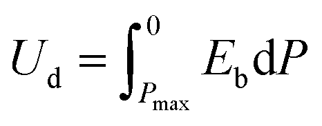
Energy has always been a requirement for the growth and development of human society in every field of life. Various energy storage devices have been developed to meet energy requirements, which include dielectric capacitors, supercapacitors, batteries, fuel cells, flow cells, etc. The Ragone diagram summarizes the power densities and energy densities of commonly used devices. The energy density of fuel cells is in the range of 150–1000 W h kg−1, which is the highest as compared to that of batteries (7–200 W h kg−1), supercapacitors (0.05–15 W h kg−1), and dielectric capacitors (0.01–0.06 W h kg−1). On the other hand, the power densities follow the reverse order: fuel cells (3–200 W kg−1) < batteries (5–500 W kg−1) < supercapacitors (8–106 W kg−1) < dielectric capacitors (3 × 10³–107 W kg−1).1,2 Thus, among different energy storage devices, the dielectric or electrostatic capacitors are extremely important because of their high power density, extremely low equivalent series resistance (ESR), inherent stability at high frequencies, and ease of handling. These capacitors find applications in numerous fields such as electronic circuits (filters/rectifiers, coupling/decoupling, tuning, timing, and bypass), power electronics (commutation and snubbers), pulsed power applications (weapons: military, marine, aerospace, and explosives), medical devices, lighting (fluorescent lamps and discharge lamps) and automotive industries.3,4 The commercially available biaxially oriented polypropylene (BOPP) capacitor showed a high breakdown strength of ∼6400 kV cm−1, but it suffers from a low dielectric constant and hence low energy density (1–1.2 J cm−3).5 Thus, there is an urgent need to develop low-cost and highly efficient dielectric capacitors to meet the next-generation energy requirements.An ideal dielectric should exhibit a high dielectric constant (εr) or polarization (P) as well as high breakdown strength (Eb) for high energy density (Ud), as given by eqn (1),6
 | (1) |
Researchers have used different nanofillers such as barium titanate (BT), titanium dioxide (TiO2), etc. of different aspect ratios including 0-dimensional (e.g. nanoparticles (NPs)), 1-dimensional (e.g. nanowires (NWs), nanotubes (NTs), and nanofibers (NFs)) and 2-dimensional nanostructures (e.g. graphenes and boron nitride nanosheets (BNNSs)).7–11 It was found that large dimensional nanofillers have lower percolation thresholds and require a low amount of loading to achieve a desired dielectric performance. In this work, one-dimensional BT NFs are selected as nanofillers owing to their high dielectric constant (>1000 at 1 kHz) and large aspect ratios that enable very low loading for the desired dielectric properties.12,13 In a polymer nanocomposite, apart from nanofillers, suitable polymer selection is also an important aspect for improving the dielectric performance. Different polymers, such as polypropylene (PP), polymethyl methacrylate (PMMA), epoxy, and polyvinylidene fluoride (PVDF) and its co/terpolymers, have been used for dielectric capacitor applications because of their reasonably high Eb.
Among them, PVDF as a polymer matrix is the most studied material for dielectric capacitor applications. It is a semi-crystalline polymer (crystallinity: 50–70%) having a high dielectric constant (∼10 at 1 kHz), low loss tangent (0.04 at 1 kHz), and high breakdown strength (>3000 kV cm−1). Different C–F and C–H configurations in the chain help in forming four main different phases, viz., α (TGTG′), β (TTT), γ (T3GT3G′), and δ (TGTG′). While α, γ, and δ phases have dipole moments of 1.20 and 1.02 D in the perpendicular and parallel direction to the chain, respectively, the β-phase has dipoles arranged perpendicular to the chain axis, and this is responsible for the maximum dipole moment (2.10 D per chain per repeat unit) and hence it is easily polarizable under an external electric field. Furthermore, easily processable characteristics make PVDF attractive to be used as a polymer matrix.12,14–17
Recently, multi-layered polymer nanocomposite-based capacitors have been found to provide better dielectric performance than traditional single-layered nanocomposites as the interfaces between nanofillers and polymers as well as among different layers of the films help in increasing the polarization and simultaneously act as a barrier to block the path of electrical stress across the film, thereby increasing the breakdown strength and hence energy density. The literature suggests that researchers have explored different approaches to improve dielectric performance in a multi-layered capacitor. Nanofillers of different contents and aspect ratios and a suitable combination of high breakdown strength and high dielectric constant layers helped in enhancing the dielectric properties. Different fabrication methods, such as hot-pressing, help in removing the air-traps and making the overall film more homogeneous. Also, a different number of layers further improves the energy density.12,18–24 However, none of the research has focused on interface modulation between different layers of the multi-layered films. Thus, the present work provides an insight towards improving the interface using a linker layer, as in core@shell nanofiller/polymer type devices,5 which helps in the binding of the top and bottom layers of the films and improving the dielectric performance.
In this study, we have designed BT NFs/PVDF sandwiched polymer nanocomposites with polyvinyl pyrrolidone (PVP) in the middle layer using a simple spin-coating method. The top and bottom BT NFs/PVDF (B) layers act as polarization layers to induce a high dielectric constant while the middle PVP (P) layer acts as a linker as well as an insulating layer to achieve both high electrical displacement and high breakdown strength by blocking the breakdown paths in the outer B layers. The results showed that the maximum energy density of 8.7 J cm−3 at 210 MV m−1 was obtained at 1 vol% BT loading in the top and bottom B layers. This work also demonstrates that the interface modulation on a larger scale has the potential to improve the dielectric performance inspired by the use of linkers in core@shell nanofillers in the polymer matrix and will enable low-cost and large-scale production of capacitor devices for efficient energy harvesting.
Experimental
Materials
Barium acetate (Ba(OAc)2, ACS reagent, 99%), titanium(IV) isopropoxide (TTIP, 97%), and polyvinylidene fluoride (PVDF) (MW: ∼534![[thin space (1/6-em)]](https://www.rsc.org/images/entities/char_2009.gif) 000 by gel permeation chromatography) were provided by Aldrich. Polyvinylpyrrolidone (PVP, MW: 1300000) was obtained from Alfa Aesar. N,N-Dimethylformamide (DMF), ethanol (ACS, Emsure), and glacial acetic acid (for chromatography) were supplied by Merck. All the chemicals were used as-received without further purification. Indium tin oxide (ITO) coated glass substrates (15 Ω) were collected from Lumtec, Taiwan.
000 by gel permeation chromatography) were provided by Aldrich. Polyvinylpyrrolidone (PVP, MW: 1300000) was obtained from Alfa Aesar. N,N-Dimethylformamide (DMF), ethanol (ACS, Emsure), and glacial acetic acid (for chromatography) were supplied by Merck. All the chemicals were used as-received without further purification. Indium tin oxide (ITO) coated glass substrates (15 Ω) were collected from Lumtec, Taiwan.
Synthesis of BT NFs
The BT nanofibers were synthesized by electrospinning as follows (Fig. 1a).25 First, 1.275 g of Ba(OAc)2 was dissolved in 3 mL of acetic acid by stirring at 50 °C for 2 h followed by the addition of an equimolar solution of 1.475 mL of TTIP. The mixture was stirred for 10 min until the solution became transparent. To control the viscosity of the ceramic precursor solution, 200 mg of PVP in 3 mL of ethanol was added dropwise to the above solution, and the mixture was stirred for 1 h. The resulting homogeneous solution was electrospun. The electrospinning parameters were as follows: applied voltage at the needle tip = 15 kV, solution flow rate = 2 mL h−1, the distance between the syringe needle tip and the collector = 7 cm, and collector rpm = 300. The collected fibers were dried in a hot air oven at 60 °C for 12 h followed by calcination at 750 °C for 2 h to get dense BT ceramic nanofibers.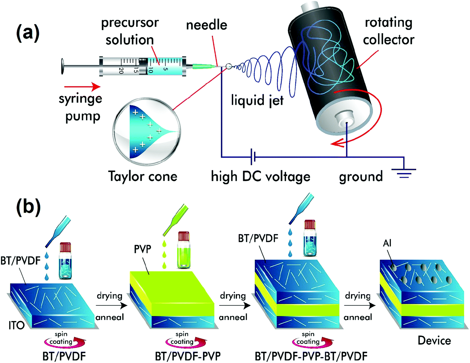 | ||
| Fig. 1 Schematics for (a) the synthesis of BT NFs using an electrospinning technique, and (b) steps for the device fabrication of sandwich multilayered films. | ||
Device fabrication
The sandwich-structured nanocomposite films were prepared using a layer-by-layer spin-coating method as described (Fig. 1b). The BT NFs were dispersed in DMF followed by the addition of PVDF (0.1 g mL−1) and stirred at 60 °C for 24 h to form a stable suspension. The solution was spin-coated at 2000 rpm for 1 min on ITO coated glass substrates and dried at 60 °C on a hot-plate for 4 h, then dried in a vacuum oven for 24 h, and annealed at 180 °C for 10 min. Similarly, the layer-by-layer assembly of PVP (30 mg mL−1) and BT NFs/PVDF in the middle and top layers, respectively, was performed. The resultant BT NFs/PVDF-PVP-BT NFs/PVDF (abbreviated as BPB) films have a typical thickness of 2–3 μm. The aluminium (Al) electrodes of 1 mm diameter were thermally deposited by thermal deposition to act as top-electrodes while ITO served as the bottom electrode for electrical measurements.Characterization
The morphological information of the as-prepared BT NFs, as well as device structure, was obtained via field emission scanning electron microscopy (FESEM, Quanta 200, Zeiss, Germany). The crystalline phase of the nanomaterials was confirmed via X-ray diffraction (XRD, PANalytical, Cu Kα radiation with λ = 1.5406 Å) and the chemical structure was confirmed via Fourier transform infrared (FTIR) spectroscopy using the KBr pellet method. The dielectric constant and the loss tangent were measured using an E4980AL Precision LCR meter (Keysight, Singapore) in the frequency range of 100 Hz to 1 MHz at room temperature. The breakdown strength and hysteresis loops for energy density and efficiency calculations were obtained from the Precision 4 kV HVI test system (Radiant Technologies Inc., hysteresis time: 10 ms). The film thicknesses were measured using a DektakXT, Bruker, surface profilometer. The Al electrodes were deposited using a HINDVAC thermal evaporator (model no. 12A4D-T, Bangalore, India).Results and discussion
The FESEM images unveil that the as-synthesized BT NFs have large aspect ratios with an average diameter of 184 nm (Fig. 2a and b). The XRD patterns show that the BT NFs are in the cubic crystalline phase and represent good crystallinity as confirmed by ICDD file number 81-2202 (Fig. 2c). The FTIR spectra show a broad low-intensity peak at 3440, and a peak at 1640 cm−1, which are associated with the surface adsorbed stretching and chemisorbed bending vibration of water, respectively (Fig. 2d). Also, the peaks at 1142 and 1060 cm−1 are due to –OH groups. The sharp peaks at 1435 and in the range of 400–850 cm−1 represent Ti–O stretching.6,26,27 The small doublet peaks at 2923 and 2854 cm−1 are assigned to asymmetric and symmetric –CH2 vibrations, respectively.28 This confirms the successful synthesis of BT NFs to be used as nanofillers in capacitor devices.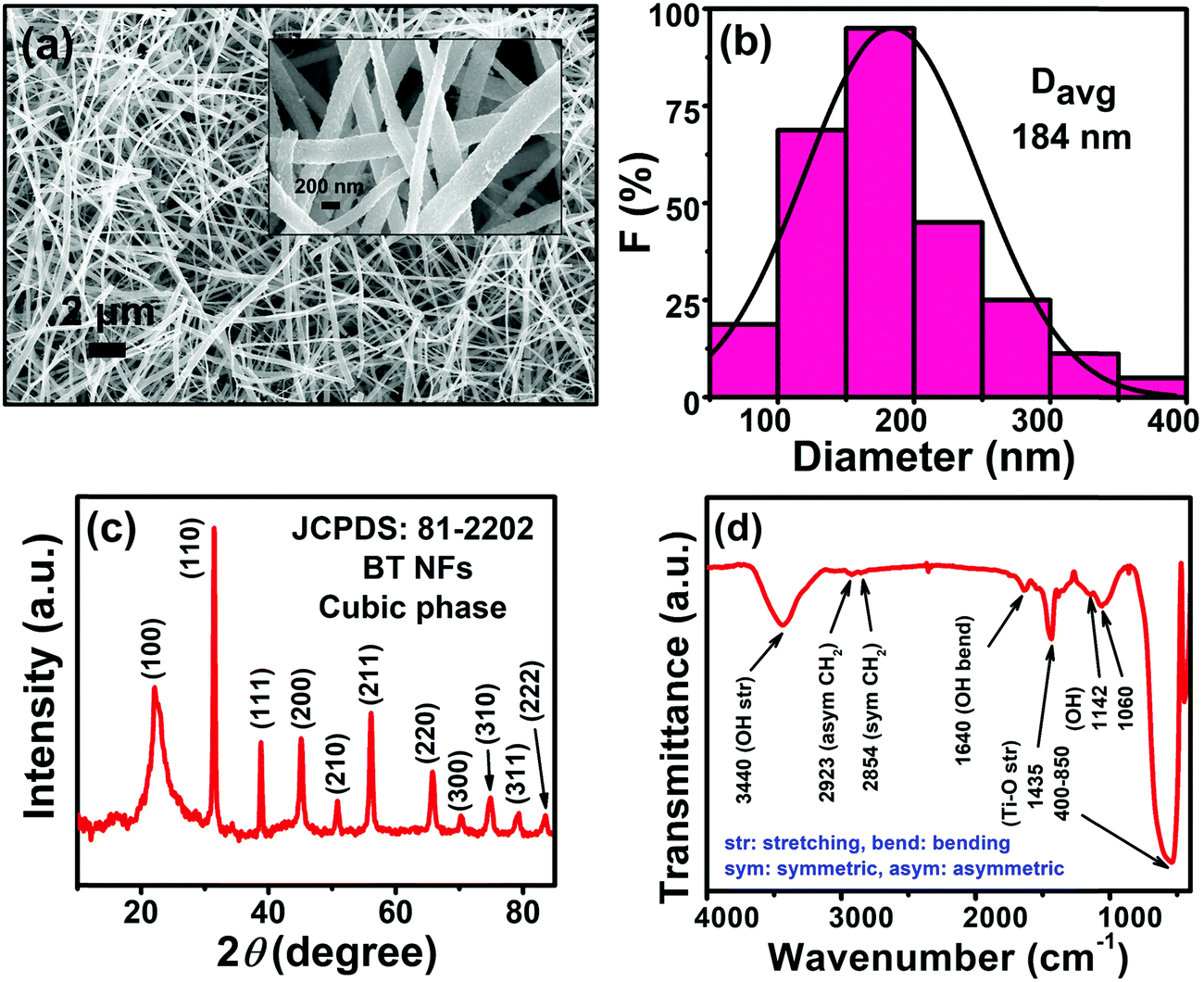 | ||
| Fig. 2 (a) FESEM image (the inset shows a magnified image), (b) size-distribution, (c) XRD pattern, and (d) FTIR spectra of BT NFs. | ||
The dielectric study was performed to study the role of the linker in the middle layer and different nanofiller contents in the top and bottom layers. The devices are abbreviated as x vol% BPB for x vol% BT NF loadings in the top and bottom layers and PVP in the middle layer. Fig. 3a shows the dielectric constant variation with a change in frequency. It can be seen that the dielectric constant increases with BT NF loading and follows the order: 9.0 (PVDF) < 9.1 (0.1 vol% BPB) < 9.3 (1 vol% BPB) < 10.4 (3 vol% BPB) < 10.9 (5 vol% BPB) at 1 kHz. The increase in dielectric constant at lower loadings of 0.1 and 1 vol% is less significant and further increases at 3 and 5 vol% are due to the addition of high dielectric constant BT NFs and more charge accumulation in the devices. Moreover, the dielectric constant decreases with a decrease in frequency, which suggests that the dipoles do not follow this trend with an increase in frequency. The loss tangent (tanδ) shows two types of behaviour in the low and high-frequency range (Fig. 3b). In between 102 and 104 Hz, the loss tangents are due to relaxation in the crystalline domain of PVDF (αc relaxation). The loss tangent remains ∼0.03 at 1 kHz, which is associated with lower conduction losses. However, in the higher frequency range of 104–106 Hz, the loss tangent decreases with an increase in loading from 0.1 to 1 vol% and further increases with BT NF loading.
 | ||
| Fig. 3 (a) Dielectric constant (εr) and (b) loss tangent (tanδ) of different devices. | ||
The lower loss tangents of ∼0.18 at 1 MHz for 0.1 and 1 vol% loading as compared to 0.25 for pure PVDF are due to the reduced polymer content as well as the restricted segmental motion of the amorphous phase of PVDF (αa relaxation). The further increase in loss tangents to ∼0.32 at 1 MHz for 3 and 5 vol% loading suggests that the nanofiller contribution dominates at higher loading, which increases the inhomogeneity and charge accumulation at the interfaces between nanofillers/polymers as well as different layers of the films, thereby contributing to more losses.29–31
Another important parameter in evaluating the dielectric performance and reliability of the capacitors is the characteristic breakdown strength (eqn (1)). It is calculated using two-parameter Weibull statistics as follows (eqn (2), Fig. 4a and b):32
 | (2) |
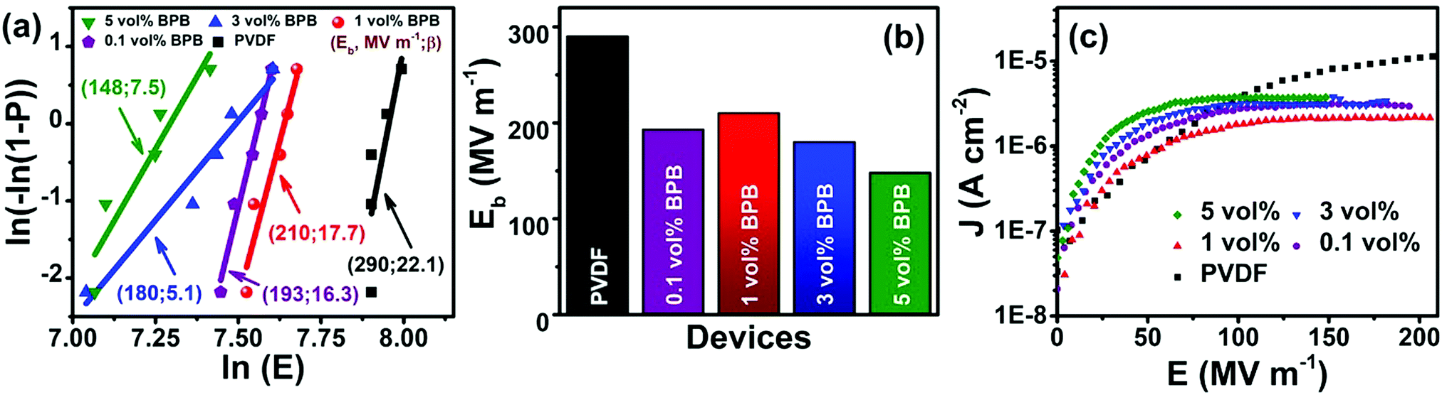 | ||
| Fig. 4 (a) Weibull analysis, (b) characteristic breakdown strength (Eb), and (c) current density (J) vs. electric field (E) of all the devices. | ||
Fig. 4a and b show the Weibull analysis of different devices. It can be seen that the breakdown strength is maximum for pure PVDF (290 MV m−1) and it decreases to 193 MV m−1 with the increase in loading to 0.1 vol% in BPB. The addition of 0.1 vol% BT NFs in a multi-layered architecture increases the space-charge flow because of possible structural defects and charge accumulation in the top and bottom layers and it facilitates the formation of electrical trees, which is also confirmed by the increase in leakage current, as seen in Fig. 4c (here, the J vs. E curve of PVDF is shown up to 210 MV m−1 for better comparison while that for Eb is shown in Fig. S1, ESI†). Among different multi-layered polymer nanocomposites, the maximum breakdown strength of 210 MV m−1 is obtained at 1 vol% loading, which further decreases with the addition of nanofillers associated with an inhomogeneous electric field and more chances of the formation of conducting pathways, thereby inducing more leakage current. Also, 1 vol% BPB exhibits a higher β value of 17.7, which further decreased with BT NF loadings in 3 and 5 vol% BPB, suggesting a higher degree of reliability.
The reason for the enhanced breakdown strength for 1 vol% BPB as compared to that of the other devices is as follows. The BT NFs in the top and bottom layers form homogeneous interfaces due to hydrogen bonding and this reduces the inhomogeneity in these layers, while the middle PVP layer strongly forms dipole–dipole interaction with these layers thereby making the overall film more homogeneous as compared to other devices (Fig. 7a). Moreover, the PVP linker in the middle layer and PVDF in the outer BT NFs/PVDF layers are optimum to act as barriers and confine the space charges in the traps and boundaries of the lamellar-crystal as well as interlamellar-amorphous regions of the polymers. The minimum leakage current at 1 vol% BPB also suggests the reduced mobility of free charge carriers in the films leading to maximum breakdown strength.9,33–35
The dielectric performance of the sandwiched polymer nanocomposites was studied by analyzing the polarization (P)–electric field (E) loops, as shown in Fig. 5a and b. To achieve a high energy density, the polarization and breakdown strength should be high along with minimum remnant polarization. Fig. 5b shows that the P–E loops are approximately of linear-type with low remnant polarization, which is beneficial in harvesting high energy density. The energy density of different devices was calculated, as shown in Fig. 5c (eqn (1)). It can be seen that 1 vol% BPB shows the maximum energy density of 8.7 J cm−3 at 210 MV m−1, which is ∼400% higher than that of pure PVDF at the same field. Since 1 vol% BPB shows the highest Eb, it can be polarized to higher fields as compared to the other composites. Moreover, a much-enhanced electric polarization of ∼10.5 μC cm−2 as compared to 2.4 μC cm−2 for pure PVDF further helps in enhancing the energy density. The low remnant polarization at optimum loading is attributed to the hydrogen bonding and dipole–dipole interaction between BT NFs/PVDF and the middle PVP layer with the top and bottom layers, which restricts the dipole rotation at higher fields. However, with an increase in nanofiller loading, the remnant polarization registers a slight increase due to the sizeable remnant polarization of nanofillers and this is, hence, responsible for the comparatively more hysteresis loss or low discharged energy density.
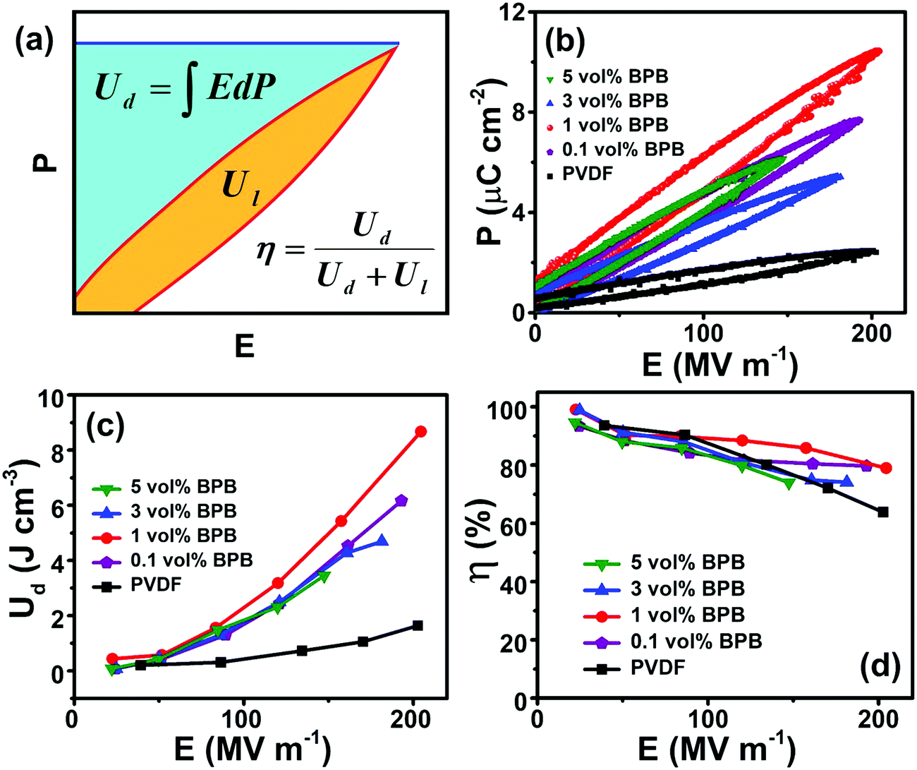 | ||
| Fig. 5 (a) Schematics of polarization (P) versus electric field (E) loop, (b) P–E loops, (c) energy density (Ud) versus E, and (d) efficiency (η) versus E of different devices. | ||
Apart from energy density, another important parameter in evaluating the device performance is the efficiency η as given in eqn (3),35
 | (3) |
Furthermore, a comparison of the energy density and efficiency of 1 vol% BPB with single layered 1 vol% BT NFs/PVDF (1 vol% B) and bi-layered 1 vol% BT NFs/PVDF-BT NFs/PVDF (1 vol% BB) shows that the addition of a linker significantly improved the energy density, which is associated with improved interfacial polarization (Fig. S2, ESI†). It can be seen that the energy densities of the 1 vol% B and 1 vol% BB devices are ∼2.0, and ∼1.7 J cm−3 at ∼210 MV m−1, respectively, while the efficiencies were reduced from 80% in 1 vol% BPB to ∼50 and ∼58% for 1 vol% B and 1 vol% BB, respectively. Thus, linker addition is beneficial towards achieving enhanced dielectric performance.
Role of the PVP linker in the middle-layer for improved dielectric performance
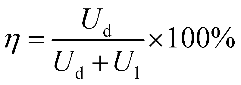
The improved dielectric performance of the 1 vol% BPB device can be explained as follows. The devices are fabricated using a simple spin-coating approach without applying high pressure and temperature as in hot-pressing and we aim to reduce the device irregularities along with an increase in dielectric performance.In a bi-layered BB polymer nanocomposite without PVP in the middle layer (Fig. 6a), there are mainly two types of interfaces in the film, i.e., in between the BT NFs/polymer and top/bottom layers (B/B). When an external field is applied, the electrons are ejected out from the electrodes causing the dielectric material to polarize and block these mobile electrons from passing through it up to the breakdown electric field. Fig. 6a shows that the interface at B/B is relatively non-homogeneous and associated with defects as well as traps for the same BT NF loading. Thus, the air voids present inside the top and bottom layers as well as at the interface between these layers undergo local breakdown due to the lower breakdown of air (3 MV m−1) leading to local heating and degradation of film quality.36 This results in the formation of conducting channels across the film at higher electric fields and is responsible for the early breakdown.
 | ||
| Fig. 6 Schematics showing the mechanism of charge movement (a) without PVP in the BB device and (b) with PVP in the BPB device; and (c) cross-sectional FESEM image of the 1 vol% BPB device. | ||
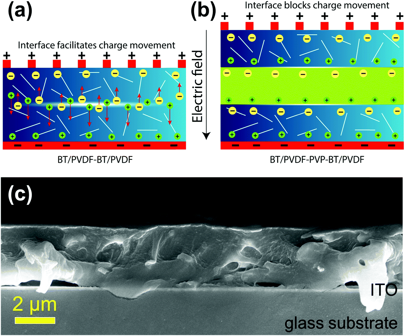
So, the interface was modulated using a PVP linker to study the dielectric performance (Fig. 6b). The PVP linker has the following roles in determining the dielectric performances. First, the FTIR spectra of PVDF and PVDF–PVP are shown in Fig. 7a. The PVDF shows peaks at 612 (bending and wagging vibrations of CF2) as well as 764 cm−1 (rocking vibration of PVDF), which shows that the PVDF is present in α-phase.31 Additional peaks at 410, 486 and 531 confirm the presence of α-PVDF.37 A careful examination of FTIR spectra shows that there is a shift in the peak from 1631 in PVDF to 1643 cm−1 in PVDF–PVP, which shows the strong dipole–dipole interaction of C–F (PVDF)⋯C![[double bond, length as m-dash]](https://www.rsc.org/images/entities/char_e001.gif) O (PVP). Moreover, a slight decrease in wavenumber of the OH peak from 3435 cm−1 in PVDF to 3430 cm−1 in PVDF–PVP suggests the formation of hydrogen bonds between them.38 The PVP helps in making a homogeneous interface between top and bottom layers by removing the defects and air traps through strong dipole–dipole interaction and hydrogen bonding between PVP and PVDF.39 It is also clear from the cross-sectional FESEM image of the 1 vol% BPB device (Fig. 6c) that the BT NFs are uniformly dispersed in the outer layers and the overall device is homogeneous without any defects or gaps at the interface. The thickness of the PVP is very small and cannot be observed during imaging but suitably works as an adhesive to link the top and bottom layers. The important consequence of the robust interface is the reduced remnant polarization and hence low hysteresis losses.5,40,41 Second, the overall electric field is also lowered due to counter-charges in each layer of the film. Thus, the formation of electrical trees is suppressed due to the homogeneous electric field.
O (PVP). Moreover, a slight decrease in wavenumber of the OH peak from 3435 cm−1 in PVDF to 3430 cm−1 in PVDF–PVP suggests the formation of hydrogen bonds between them.38 The PVP helps in making a homogeneous interface between top and bottom layers by removing the defects and air traps through strong dipole–dipole interaction and hydrogen bonding between PVP and PVDF.39 It is also clear from the cross-sectional FESEM image of the 1 vol% BPB device (Fig. 6c) that the BT NFs are uniformly dispersed in the outer layers and the overall device is homogeneous without any defects or gaps at the interface. The thickness of the PVP is very small and cannot be observed during imaging but suitably works as an adhesive to link the top and bottom layers. The important consequence of the robust interface is the reduced remnant polarization and hence low hysteresis losses.5,40,41 Second, the overall electric field is also lowered due to counter-charges in each layer of the film. Thus, the formation of electrical trees is suppressed due to the homogeneous electric field.
 | ||
| Fig. 7 (a) FTIR spectra of PVDF and PVP and their interaction and (b) current density (J) vs. electric field (E) variation for 1 vol% BB and 1 vol% BPB devices. | ||
Third, the overall number of interfaces in BPB is more than that in the BB polymer nanocomposites as PVP itself acts as an insulating layer resulting in an enhancement in interfacial polarization through the confinement of interfacial charges in each layer, thereby increasing the polarization as well as breakdown strength.5,35,42 This is also supported by the fact that the 1 vol% BB device exhibits comparatively higher leakage current density and makes the charge transport more feasible, which decreases with the addition of PVP for the 1 vol% BPB device (Fig. 7b). Thus, PVP entraps the space charges, restricts their movement across the layers, and helps in improving the dielectric characteristics.
However, for the same PVP content, the increase in BT NF loadings in the outer B layers adversely degrades the dielectric performance. At higher loadings, there are more possibilities for the formation of inhomogeneous interfaces in each layer, which increases the formation of conducting channels that combines with that of the interface leading to higher leakage current and hence lower breakdown strength.32,43 Thus, the optimum BT NF loading in the top and bottom layers, as well as the PVP linker, is helpful in increasing the energy density as well as dielectric performance.
In brief, the primary role of PVP in this work is to make the homogeneous interface free of air-voids, structural defects, and to mitigate the non-homogeneity of the electric field by reducing the local electric field concentration at the interface. The generation of the counter electric field and dipolar interactions at the PVDF–PVP interface helps in increasing the homogeneity of the electric field and is responsible for a high breakdown strength and energy density. The energy density of the present work is compared with the previous literature, as shown in Table 1. It has been found that the current work demonstrates a significant improvement in the dielectric properties with a high discharged energy density of 8.7 J cm−3 and an efficiency of 80% at the same field (∼210 MV m−1). Furthermore, nanofillers without any surface modification at a much lower loading and a simple device fabrication technique make the overall device attractive for high energy density applications.
| Nanofiller | Number of layers | Loading in each layer (vol%) | Device fabrication method | U d (J cm−3) at ∼210 MV m−1 | η (%) at ∼210 MV m−1 | Ref. |
|---|---|---|---|---|---|---|
| Abbreviations: NPs: nanoparticles, P(VDF-HFP): poly(vinylidene fluoride-co-hexafluoropropylene), BNNS: boron nitride nanosheets, BST NWs: barium strontium titanate nanowires, NBT: Na0.5Bi0.5TiO3, P(VDF–TrFE–CFE): poly(vinylidene fluoride–trifluoroethylene–chlorofluoroethylene), PTCF: P(VDF–TrFE–CFE) fiber, BZT: 0.5Ba(Zr0.2Ti0.8)O3, BCT: 0.5(Ba0.7Ca0.3)TiO3, PDA: polydopamine, and NN: NaNbNO3. | ||||||
| BT@Fe3O4 NPs/PVDF-PVDF-BT@Fe3O4 NPs/PVDF | 3 | 5–0–5 | Hot pressing | 2.2 | 60 | 44 |
| BT@hydantoin NPs/P(VDF-HFP)-P(VDF-HFP)-BT@hydantoin NPs/P(VDF-HFP) | 3 | 35–0–35 | Tape casting | 2.5 | 60 | 45 |
| BNNS/PVDF-BST NWs/PVDF-BNNS/PVDF | 3 | 10–8–10 | Hot pressing | 2.5 | 72 | 46 |
| NBT NPs/PVDF-PVDF-NBT NPs/PVDF | 3 | 1–0–1 | Solution casting | 3 | 60 | 34 |
| PVDF-PTCF-PVDF | 3 | — | Hot pressing | 3 | 65 | 47 |
| BZT-BCT NFs@PDA/PVDF-BNNS@Fe3O4@PDA/PVDF-BZT-BCT NFs@PDA/PVDF | 3 | 3–5–3 | Hot pressing | 3.5 | 65 | 48 |
| NN platelets@PDA/PVDF-PVDF-NN platelets@PDA/PVDF | 3 | 5–0–5 | Solution casting | 3.7 | 75 | 49 |
| BT NPs/PVDF-BT NPs/PVDF-BT NPs/PVDF | 3 | 20–1–20 | Solution casting | 4 | 55 | 21 |
| PVDF-BZT@BCT@CoFe2O4 NFs/PVDF-PVDF | 3 | 0–5–0 | Hot pressing | 4.2 | 70 | 50 |
| BT NPs@PDA/PVDF-PVDF-BT NPs@PDA/PVDF | 3 | 7–0–7 | Solution casting | 4.5 | 63 | 30 |
| BT NPs/P(VDF-HFP)-BT NPs/P(VDF-HFP)-BT NPs/P(VDF-HFP) | 3 | 1–9–1 | Solution casting | 5 | 75 | 51 |
| BT NPs/PVDF-BT NPs/PVDF-BT NPs/PVDF | 3 | 20–10–1 | Solution casting | 5 | 70 | 52 |
| PVDF-BT@TiO2@PDA NFs/P(VDF–TrFE–CFE)-PVDF | 3 | 0–15 wt%-0 | Hot pressing | 5 | 70 | 53 |
| BNNS/P(VDF-HFP) | 12 | 1–0–1–0⋯0–1–0–1 | Hot pressing | 7 | 20 | 22 |
| BT NFs/PVDF-PVP-BT NFs/PVDF | 3 | 1–0–1 | Solution casting | 8.7 | 80 | This work |
Conclusions
In summary, BT NFs/PVDF based sandwich structured nanocomposites were successfully prepared, and a large enhancement in the energy density has been demonstrated at a much lower electric field through a homogeneous interface using the simple spin coating method. The sandwiched structure improved the polarization due to BT NFs in the top and bottom layers. The PVP in the middle layer helped in forming a homogeneous interface via strong dipole–dipole interaction and hydrogen bonding with the outer layers and is responsible for the enhanced breakdown strength, energy density and efficiency along with reduced remnant polarization and leakage current. The composite with 1 vol% loading showed an energy density of 8.7 J cm−3 (efficiency = 80%) at 210 MV m−1, which is ∼400 and ∼800% higher than that of single-layered PVDF and commercially available BOPP, respectively. The present work has the potential to meet the requirements of next-generation efficient and low-cost dielectric capacitors using a simple device fabrication method.Conflicts of interest
There are no conflicts of interest to declare.Acknowledgements
Financial support from the Department of Atomic Energy (DAE), BRNS, India for grant 34/14/14/2014-BRNS and the Department of Science and Technology (DST) Grant No. DST/TMD/CERI/C140(G) under Clean Energy Research Initiative is acknowledged. AG acknowledges the financial support through the Imprint (II) project (IMP/2018/001703) from the Science and Engineering Research Board (Government of India). RKG acknowledges the financial assistance from the DST, India, through the INSPIRE Faculty Award (Project No. IFA-13 ENG-57).References
- A. Braun, in Electrochemical Energy Systems-Foundations, Energy Storage and Conversion, de Gruyter, Berlin/Boston, 2019, ch. 2, pp. 45–102 Search PubMed.
- L. Bai, Y. Zhang, W. Tong, L. Sun, H. Huang, Q. An, N. Tian and P. K. Chu, Electrochem. Energy Rev., 2020, 3, 395–430 CrossRef CAS.
- Y. Shen, X. Zhang, M. Li, Y. Lin and C.-W. Nan, Natl. Sci. Rev., 2017, 4, 23–25 CrossRef CAS.
- D. Q. Tan and Adv. Funct, Materials, 2019, 1808567, DOI:10.1002/adfm.201808567,.
- H. Luo, X. Zhou, C. Ellingford, Y. Zhang, S. Chen, K. Zhou, D. Zhang, C. R. Bowen and C. Wan, Chem. Soc. Rev., 2019, 48, 4424–4465 RSC.
- Prateek, R. Bhunia, S. Siddiqui, A. Garg and R. K. Gupta, ACS Appl. Mater. Interfaces, 2019, 11, 14329–14339 CrossRef CAS PubMed.
- W. Meng, Y. Huang, Y. Fu, Z. Wang and C. Zhi, J. Mater. Chem. C, 2014, 2, 10049–10061 RSC.
- Q. Li, F. Liu, T. Yang, M. R. Gadinski, G. Zhang, L.-Q. Chen and Q. Wang, Proc. Natl. Acad. Sci. U. S. A., 2016, 113, 9995 CrossRef CAS PubMed.
- Z. Pan, L. Yao, J. Zhai, K. Yang, B. Shen and H. Wang, ACS Sustainable Chem. Eng., 2017, 5, 4707–4717 CrossRef CAS.
- X. Zhang, Y. Shen, Q. Zhang, L. Gu, Y. Hu, J. Du, Y. Lin and C.-W. Nan, Adv. Mater., 2015, 27, 819–824 CrossRef CAS PubMed.
- B. Jiang, J. Iocozzia, L. Zhao, H. Zhang, Y.-W. Harn, Y. Chen and Z. Lin, Chem. Soc. Rev., 2019, 48, 1194–1228 RSC.
- Prateek, V. K. Thakur and R. K. Gupta, Chem. Rev., 2016, 116, 4260–4317 CrossRef CAS PubMed.
- H. Zhang, M. A. Marwat, B. Xie, M. Ashtar, K. Liu, Y. Zhu, L. Zhang, P. Fan, C. Samart and Z.-G. Ye, ACS Appl. Mater. Interfaces, 2020, 12, 1–37 CrossRef CAS PubMed.
- Q. Chen, Y. Shen, S. Zhang and Q. M. Zhang, Annu. Rev. Mater. Res., 2015, 45, 433–458 CrossRef CAS.
- B. Fan, M. Zhou, C. Zhang, D. He and J. Bai, Prog. Polym. Sci., 2019, 97, 101143 CrossRef CAS.
- P. Martins, A. C. Lopes and S. Lanceros-Mendez, Prog. Polym. Sci., 2014, 39, 683–706 CrossRef CAS.
- N. A. Shepelin, A. M. Glushenkov, V. C. Lussini, P. J. Fox, G. W. Dicinoski, J. G. Shapter and A. V. Ellis, Energy Environ. Sci., 2019, 12, 1143–1176 RSC.
- Y. Wang, J. Chen, Y. Li, Y. Niu, Q. Wang and H. Wang, J. Mater. Chem. A, 2019, 7, 2965–2980 RSC.
- J. Jiang, Z. Shen, J. Qian, Z. Dan, M. Guo, Y. Lin, C.-W. Nan, L. Chen and Y. Shen, Energy Storage Mater., 2019, 18, 213–221 CrossRef.
- P. Hu, Y. Shen, Y. Guan, X. Zhang, Y. Lin, Q. Zhang and C.-W. Nan, Adv. Funct. Mater., 2014, 24, 3172–3178 CrossRef CAS.
- Y. Wang, J. Cui, Q. Yuan, Y. Niu, Y. Bai and H. Wang, Adv. Mater., 2015, 27, 6658–6663 CrossRef CAS PubMed.
- Y. Zeng, Z.-H. Shen, Y. Shen, Y. Lin and C.-W. Nan, Appl. Phys. Lett., 2018, 112, 103902 CrossRef.
- Z. Sun, L. Wang, M. Liu, C. Ma, Z. Liang, Q. Fan, L. Lu, X. Lou, H. Wang and C.-L. Jia, J. Mater. Chem. A, 2018, 6, 1858–1864 RSC.
- Q. Chi, Z. Gao, T. Zhang, C. Zhang, Y. Zhang, Q. Chen, X. Wang and Q. Lei, ACS Sustainable Chem. Eng., 2019, 7, 748–757 CrossRef CAS.
- J. Yuh, J. C. Nino and W. M. Sigmund, Mater. Lett., 2005, 59, 3645–3647 CrossRef CAS.
- A. A. Aal, T. R. Hammad, M. Zawrah, I. K. Battisha and A. B. A. Hammad, Acta Phys. Pol., 2014, 126, 1318–1321 CrossRef.
- S. Cho, J. S. Lee and J. Jang, Adv. Mater. Interfaces, 2015, 2, 1500098 CrossRef.
- D. Olmos, E. V. Martín and J. González-Benito, Phys. Chem. Chem. Phys., 2014, 16, 24339–24349 RSC.
- Y. Wang, Y. Hou and Y. Deng, Compos. Sci. Technol., 2017, 145, 71–77 CrossRef CAS.
- Y. Wang, J. Cui, L. Wang, Q. Yuan, Y. Niu, J. Chen, Q. Wang and H. Wang, J. Mater. Chem. A, 2017, 5, 4710–4718 RSC.
- Y. N. Hao, X. H. Wang, S. O'Brien, J. Lombardi and L. T. Li, J. Mater. Chem. C, 2015, 3, 9740–9747 RSC.
- Z. Pan, L. Yao, J. Liu, X. Liu, F. Pi, J. Chen, B. Shen and J. Zhai, J. Mater. Chem. C, 2019, 7, 405–413 RSC.
- Y. Zhang, C. Zhang, Y. Feng, T. Zhang, Q. Chen, Q. Chi, L. Liu, G. Li, Y. Cui, X. Wang, Z. Dang and Q. Lei, Nano Energy, 2019, 56, 138–150 CrossRef CAS.
- W. Nian, Z. Wang, T. Wang, Y. Xiao and H. Chen, Ceram. Int., 2018, 44, S50–S53 CrossRef CAS.
- J. Chen, Y. Wang, X. Xu, Q. Yuan, Y. Niu, Q. Wang and H. Wang, J. Mater. Chem. A, 2018, 6, 24367–24377 RSC.
- Y. Niu, Y. Bai, K. Yu, Y. Wang, F. Xiang and H. Wang, ACS Appl. Mater. Interfaces, 2015, 7, 24168–24176 CrossRef CAS PubMed.
- X. Cai, T. Lei, D. Sun and L. Lin, RSC Adv., 2017, 7, 15382–15389 RSC.
- G. M. Lampman, D. L. Pavia, G. S. Kriz and J. R. Vyvyan, in Spectroscopy, Cengage Learning, India, 4th edn, 2012, ch. 2, pp. 15–104 Search PubMed.
- Prateek, R. Bhunia, A. Garg and R. K. Gupta, ACS Appl. Energy Mater., 2019, 2, 6146–6152 CrossRef CAS.
- J. Fu, Y. Hou, M. Zheng, Q. Wei, M. Zhu and H. Yan, ACS Appl. Mater. Interfaces, 2015, 7, 24480–24491 CrossRef CAS PubMed.
- Y. Zhang, Q. Chi, L. Liu, T. Zhang, C. Zhang, Q. Chen, X. Wang and Q. Lei, ACS Appl. Energy Mater., 2018, 1, 6320–6329 CrossRef.
- X. Zhang, W. Chen, J. Wang, Y. Shen, L. Gu, Y. Lin and C.-W. Nan, Nanoscale, 2014, 6, 6701–6709 RSC.
- Z. Pan, L. Yao, J. Zhai, X. Yao and H. Chen, Adv. Mater., 2018, 30, 1705662 CrossRef PubMed.
- Y. Cui, X. Wang, Q. Chi, J. Dong, T. Ma, C. Zhang and Q. Lei, J. Mater. Sci.: Mater. Electron., 2017, 28, 11900–11906 CrossRef CAS.
- H. Luo, D. Zhang, L. Wang, C. Chen, J. Zhou and K. Zhou, RSC Adv., 2015, 5, 52809–52816 RSC.
- F. Liu, Q. Li, J. Cui, Z. Li, G. Yang, Y. Liu, L. Dong, C. Xiong, H. Wang and Q. Wang, Adv. Funct. Mater., 2017, 27, 1606292 CrossRef.
- Y. Zhang, Q. Chi, L. Liu, C. Zhang, C. Chen, X. Wang and Q. Lei, APL Mater., 2017, 5, 076109 CrossRef.
- Y. Zhang, T. Zhang, L. Liu, Q. Chi, C. Zhang, Q. Chen, Y. Cui, X. Wang and Q. Lei, J. Phys. Chem. C, 2018, 122, 1500–1512 CrossRef CAS.
- Z. Pan, B. Liu, J. Zhai, L. Yao, K. Yang and B. Shen, Nano Energy, 2017, 40, 587–595 CrossRef CAS.
- Q. Chi, T. Ma, Y. Zhang, Q. Chen, C. Zhang, Y. Cui, T. Zhang, J. Lin, X. Wang and Q. Lei, ACS Sustainable Chem. Eng., 2018, 6, 403–412 CrossRef CAS.
- Y. Wang, L. Wang, Q. Yuan, J. Chen, Y. Niu, X. Xu, Y. Cheng, B. Yao, Q. Wang and H. Wang, Nano Energy, 2018, 44, 364–370 CrossRef CAS.
- Y. Wang, L. Wang, Q. Yuan, Y. Niu, J. Chen, Q. Wang and H. Wang, J. Mater. Chem. A, 2017, 5, 10849–10855 RSC.
- Y. Shen, D. Shen, X. Zhang, J. Jiang, Z. Dan, Y. Song, Y. Lin, M. Li and C.-W. Nan, J. Mater. Chem. A, 2016, 4, 8359–8365 RSC.
Footnote |
| † Electronic supplementary information (ESI) available. See DOI: 10.1039/d0ma00240b |
| This journal is © The Royal Society of Chemistry 2020 |