
 Open Access Article
 This Open Access Article is licensed under a
 Creative Commons Attribution 3.0 Unported Licence
Challenges and approaches towards upscaling the assembly of hybrid perovskite solar cells
Ahmed Esmail
Shalan
 ab
ab
aBCMaterials-Basque Center for Materials, Applications and Nanostructures, Martina Casiano, UPV/EHU Science Park, Barrio Sarriena s/n, Leioa 48940, Spain. E-mail: a.shalan133@gmail.com; ahmed.shalan@bcmaterials.net; Tel: +34 946128811
bCentral Metallurgical Research and Development Institute (CMRDI), P.O. Box 87, Helwan, Cairo 11421, Egypt
First published on 4th May 2020
Abstract
In recent times, the next-generation photovoltaic technologies have accepted perovskite solar cells (PSCs) as different auspicious candidates as a result of their persistently developing efficiencies, thus attracting significant attention from both the scientific and industrial societies. Even though PSCs are dignified toward the commercial world through the photovoltaic module scale, significant challenges confusing industrialization remain. The recent efficiency of the solution-processed PSCs has reached over 25% on a laboratory scale. However, a reproducible allocation to the upscaling techniques of these processes still requires a highly controllable perovskite film formation strategy. Different coating systems such as blade coating, slot-die coating and spray coating as well as printing pathways such as screen, inkjet, and gravure printing besides vacuum deposition and laser patterning methods have been widely used as the substitutions of spin coating towards scaling up PSCs with a large area. In the current review, we have reported the practical potential of PSCs, strategies, challenges, and approaches towards the scaling up of large-area PSC modules via different deposition techniques as well as functional materials for the device architecture.
 Ahmed Esmail Shalan | Ahmed Esmail Shalan is Juan de la Cierva Fellow at BCMaterials, Basque Center for Materials, Applications, and Nanostructures, Leioa, Spain. He obtained his BSc (2008) and MSc (2012) in Materials Science from Ain Shams University, Egypt and his PhD (2017) from Hokkaido University, Japan. He is Researcher at Central Metallurgical Research & Development Institute (CMRDI), Egypt (on leave). He obtained several awards like Egyptian Academy Prize (2018), and fellowships like DAAD fellowship (i-MEET-FAU), Germany (2013). His work has been summarized in more than 40 articles (with an h index of 19), which reflects his interest in nanotechnology and materials science for energy and environmental applications. |
1. Introduction
Solar energy direction have been changed a lot by many researchers once the perovskite materials (CH3NH3PbI3) investigated as a new light harvesting material for hybrid perovskite solar cells (PSCs).1 A power conversion efficiency (PCE) of 25.2% of these kinds of solar cells was certified in 2019, which is close to that of monocrystalline silicon cells.2 These perovskite materials have different features such as high absorption coefficient,3,4 high mobility,5–8 long balanced carrier diffusion length,7–10 and small exciton binding energy,11 which make them auspicious candidates for the fabrication of these new kinds of solar cells. Besides, there are several kinds of solar cell systems similar to organic photovoltaics,12 dye-sensitised solar cells13–20 and perovskite cells,21–26 which intent to earn the benefit of the large-scale PSC modules with low fabrication cost. PSCs with a large active area of 1 cm2 have only achieved almost 20% in the past few years, which confirms that the upscaling of the normal active area of 0.1 cm2 of these kinds of cells is mandatory for the future modules of these kinds of cells as the active area is considered as an important factor for the detection of the net efficiency.27 The transformation of the perovskite photovoltaic technology in the sequence of “lab-to-fab” becomes a trend towards scaling up PSCs.28 In fact, the active area, stability and cost of the proposed materials can be possible drawbacks for the commercial upscaling of PSCs. The active area can be affected by the series resistance of the electrodes, which results from the quality of the assembled layers via coverage and uniformity and decreases the net efficiency of the fabricated modules.29,30 Additionally, temperature, illumination and humidity may influence the assembled module stability deemed as a significant shortcoming of PSCs.31–33 Furthermore, to overcome the drawbacks encountered while using the same deposition techniques of small-area cells for upscaling, several production methodologies such as spin coating,34 blade coating,35 slot-die coating,36 and vacuum evaporation37 have been recognised to achieve large-scale and improved eminent perovskite films. Galagan and co-workers aimed to optimize the assembled modules by finding the match for active area size and PCE by studying the standard dimensions of large-area PSCs to attain good uniformity and reproducibility over the module area.38–42 In addition, they confirmed their experimental data using a theoretical DC simulation in order to get an appropriate matching between transparency and substrate sheet resistance. Herein, in this review, the advancements matters approved on effective large-area perovskite solar modules from the view of several fabrication technique, with studying the strategies and the challenges exist for this purpose will be covered and discussed.2. Structural design of devices
2.1. Perovskite solar cell architectures: configurations and technical challenges
Perovskite solar cell (PSC) device configurations are mainly classified into two groups: mesoporous and planar structures with three different types: mesoporous n–i–p, planar n–i–p and planar p–i–n structures (Fig. 1).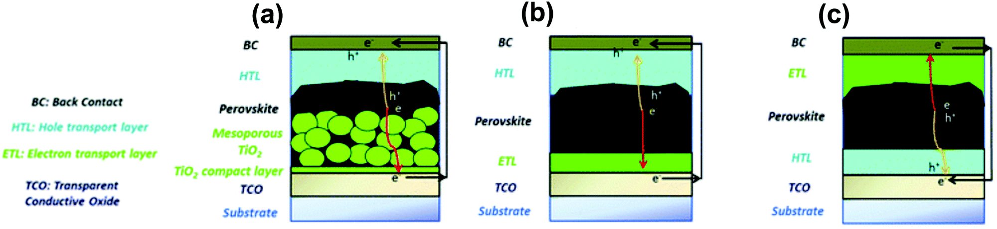 | ||
| Fig. 1 Perovskite solar cell architectures: (a) n-type TiO2 mesoporous-based; (b) planar “n–i–p”; (c) planar “p–i–n”. Illumination occurs from the substrate side. In all these cases, the substrate can be either a glass or polymer foil. Reproduced with permission from ref. 48. Copyright © 2017 The Royal Society of Chemistry. | ||
The typical mesoporous n–i–p (PSC) architecture (Fig. 1a) includes perovskite materials that are partially or completely infiltrated in an electron transport layer (ETL) scaffold with nanoscale pores, leading to an intermixed layer. After that, the hole transport layer (HTL) is deposited on the perovskite layer, and then the structure of the assembled device is completed through evaporation of the top electrode. The photocurrent–voltage (J–V) hysteresis phenomenon in PSCs can be suppressed by enhancing charge separation using mesoporous materials.43 The planar n–i–p (PSC) architecture (Fig. 1b), which has recently given high-efficiency performance with little hysteresis, is encompassed with a compact ETL layer that attaches directly to the perovskite layer without using any mesoporous layer.44–46 In the current status, the existence of mesoporous materials, and sometimes HTL, in the n–i–p cell structure is not favourable for scaling up modules, as it will increase the fabrication steps.47 Additionally, the inverted structure, p–i–n architecture (Fig. 1c), which is normally assembled with a planar structure, is coming from the inversion in the carrier extraction layers compared to the n–i–p configuration.
2.2. Perovskite solar module structures
Obviously, due to the resistance loss above the conducting electrode that may appear as a long transference expanse, the upscaling of perovskite solar modules will not be easy to attain via fabrication of a single PSC on a large-area substrate. Additionally, combining minor sub-cells with a series of interconnection areas, which act as the main aspect toward power loss in solar modules, can diminish the resistance loss to form a stable module (Fig. 2a).49 The geometric fill factor (GFF) can define the photoactive area and the total area of the module ratio, and it was found that the calculation of GFF becomes essential to detect the accurate module efficiency as the module efficiency is proportionally related to the active area as well as GFF.50 In addition, there are several steps involved in the fabrication of perovskite solar modules (PSMs).51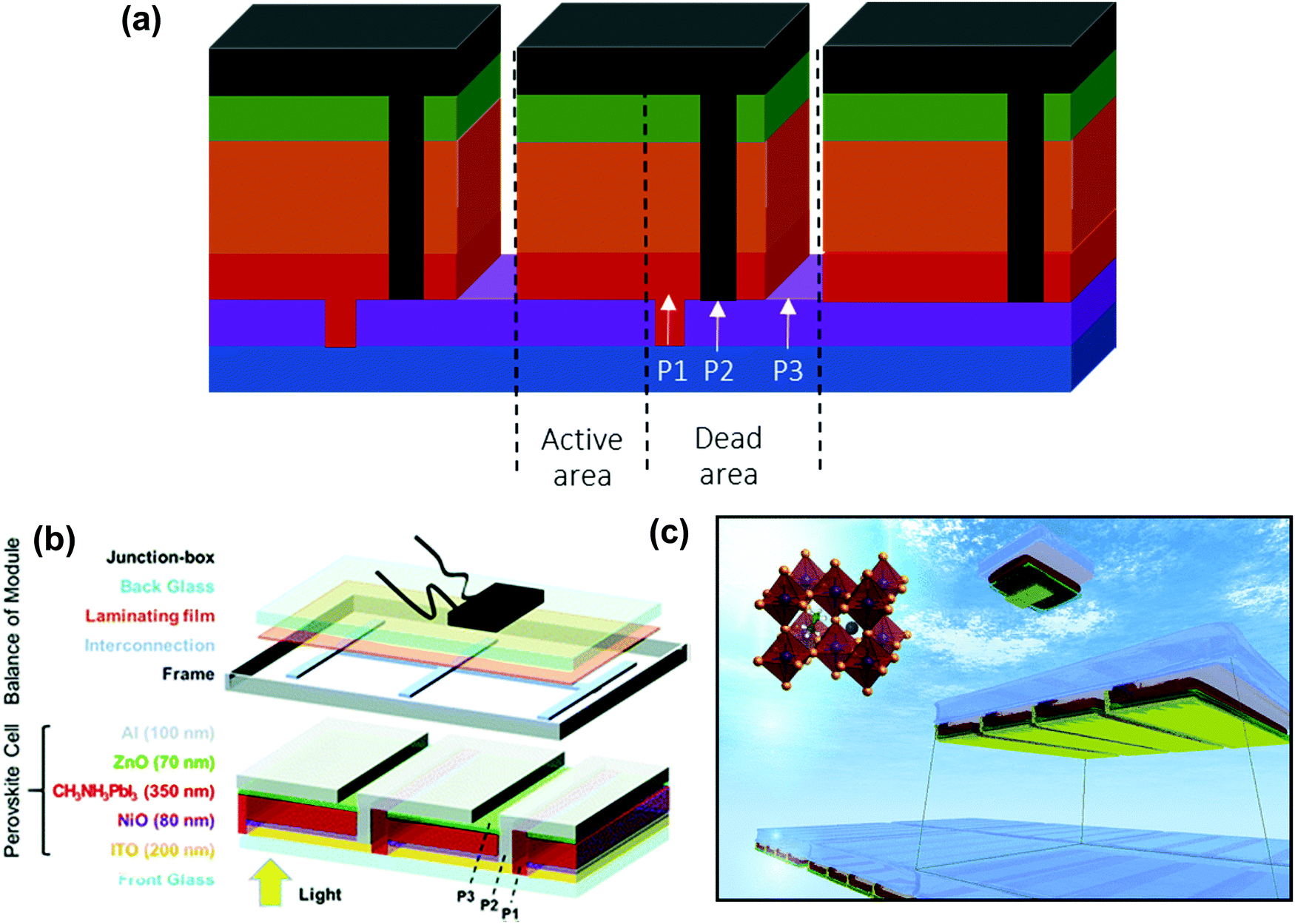 | ||
| Fig. 2 Perovskite solar module architectures. (a) Interconnection of a perovskite module fabricated by typical scribing processes for thin-film solar modules. The P1 scribe separates the bottom TCO substrate, the P2 scribe provides a channel to connect the top contact of one cell to the bottom contact of the next cell to form an interconnection, and the P3 scribe isolates the top metal contact between neighbouring cells, to form cells that can be integrated into a module. (b) Structure of a monolithically integrated perovskite solar module design with different configuration layers. Reproduced with permission from ref. 55. Copyright © 2017 The Royal Society of Chemistry. (c) Up-scaling laboratory-scale perovskite solar cells to modules and panels. Reproduced with permission from ref. 51. Copyright © 2017 American Chemical Society. | ||
Furthermore, the assembled assimilated perovskite solar module design with the altered constituent arrangement is shown in Fig. 2b. It is important that the so-called balance of module (BOM) is used to protect the fabricated modules from water-induced degradation,52 through its components including glass plates, a sealant, a lamination film, an edge-sealing frame, a junction-box, and wiring.53–55 Ultimately, the upscaling fabrication of large-area cells can be summarized via assembling high-quality perovskite cells, combining those cells to form a module and, finally, integrating the modules into a panel (Fig. 2c).
2.3. Scalable solution deposition methods
Spin coating as well as other several deposition and printing methods such as blade coating, slot-die coating, spray coating, inkjet printing and screen-printing have been widely used in the preparation of different layers for solar cell composition. The spin coating technique is considered as the traditional way for perovskite thin-film deposition. The precursor solution of perovskite materials used to fabricate the perovskite films in spin coating as well as scalable deposition methods consists of organic and lead halides, which first liquefied in organic solvents like N,N-dimethylformamide (DMF), dimethyl sulfoxide (DMSO) and γ-butyrolactone (GBL). Additionally, modules are made up via spin coating on a substrate area of about 10 cm × 10 cm but with an extensively lower PCE than their corresponding smaller area items.56 The advantages such as thinning and smoothing gained from the spin coating method for low-area film deposition are challenging to be obtained in scalable deposition processes. Therefore, in order to fabricate PSMs by controlling the assembled films in different positions, many factors should be understandable and different other pathways must be designed for increasing the active area of PSCs. Herein, different scalable solution deposition methods and their benefits for PSC and PSM improvement are briefly studied and compared.2.4. Coating techniques for perovskite photovoltaics
Besides spin coating, as forerunners for perovskite film deposition on a laboratory scale, several coating techniques are introduced in order to pave the way for upscaling PSCs and obtain PSMs by controlling the quality of perovskite films deposited above large areas with high uniform layers with good crystallinity and morphology. As meticulous below, some general competing coating methodologies will be discussed to gain deep knowledge on how these techniques are used for the fabrication of PSCs and going further on the way to upscaling PSMs to accomplish the methodological necessities for industrial approach of perovskite thin films for cells and modules.The fabrication of different layers of perovskite cells or modules by the spin coating technique is illustrated in Fig. 3a. In addition, to assemble perovskite solar cells, the conductive electrode (FTO) was etched to obtain the anticipated pattern, and then an ETL of TiO2 was deposited via the spin coating pathway. After that, the perovskite layer and the HTL were deposited layer by layer above TiO2 by the spin coating technique and finally the cell was obtained by thermal evaporation of Au on the top. The schematic of the spin coating process of the perovskite solution on the substrate surface is shown in Fig. 3b. Either the perovskite cells or modules can be fabricated by the spin coating technique, which considers being one of the essential pathways to deposit the main constituent layers.61 Additionally, the schematic design of the perovskite solar cell arrangement, where a smooth and compact perovskite capping layer fully covers the mesoporous TiO2 layer (mp-TiO2) subverted with perovskites, is shown in Fig. 3c. The mesoscopic-planar bilayer device architecture with a cross-sectional SEM image is illustrated in Fig. 3d to affirm the alteration in morphology between films in the fabricated cell.61
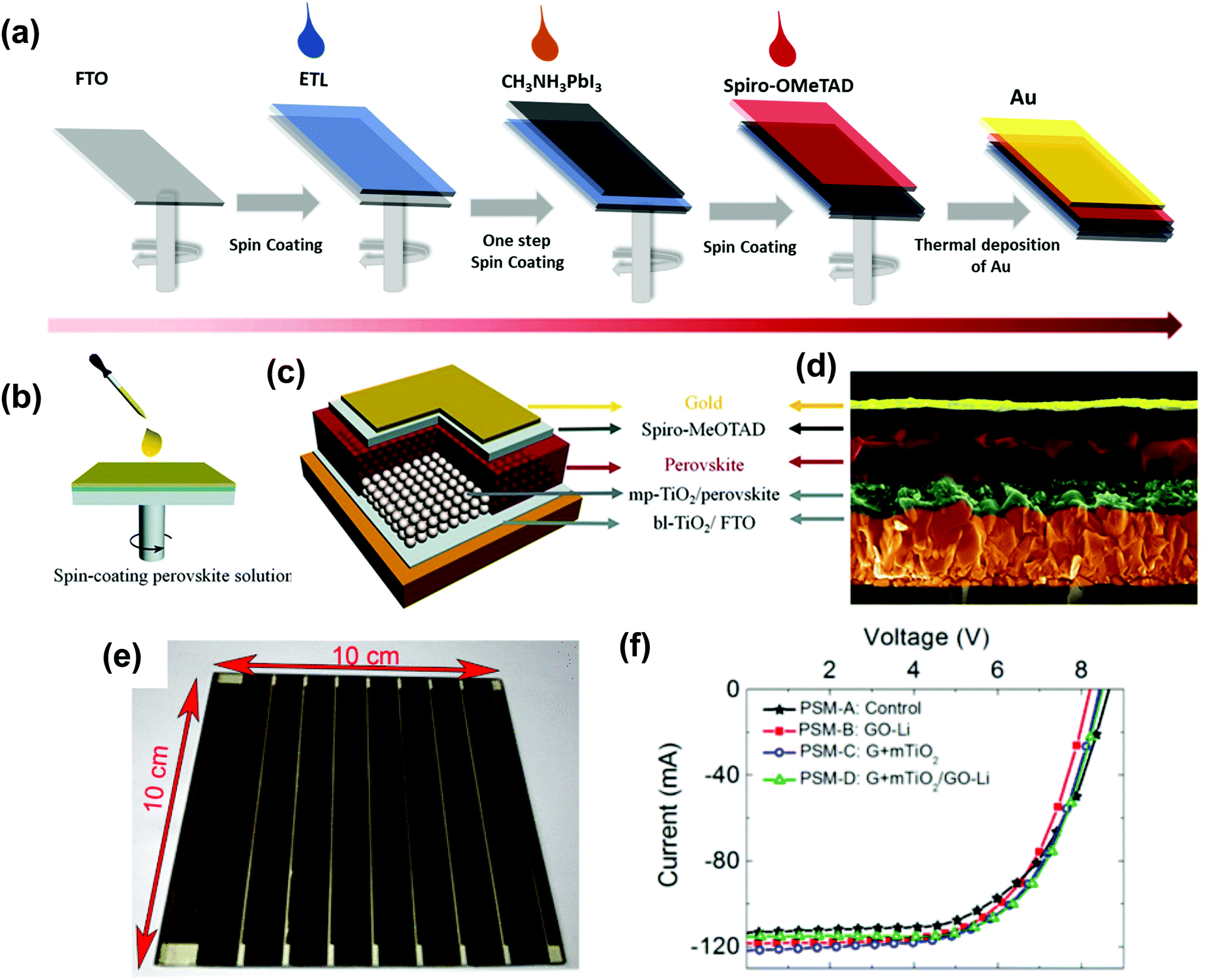 | ||
| Fig. 3 Perovskite film deposition and device structure. (a) Schematic of perovskite solar devices step by step. (b) Schematic showing the spin coating of the perovskite solution on the substrate. (c) Schematic of the perovskite solar cell configuration, where a smooth and compact perovskite capping layer fully covers the mesoporous TiO2 layer (mp-TiO2) infiltrated with perovskites. (d) A high-resolution cross-sectional SEM image of a complete perovskite solar cell with large area fabricated by the spin coating technique. (b–d) Reproduced with permission from ref. 61. Copyright © 2016 SpringerNature. (e) Photograph of the large-area perovskite solar module (50 cm2 active area). (f) Current–voltage (I–V) characteristics of tested modules (i.e., PSM-A, PSM-B, PSM-C, and PSM-D). All the I–V measurements refer to the encapsulated devices. (e and f) Reproduced with permission from ref. 62. Copyright © 2016 American Chemical Society. | ||
One of the latest studies that concern about the production of perovskite modules with large active area by the spin coating technique was done by Di Carlo et al.62 They established large-area perovskite solar modules (PSMs), assembled on a 10 × 10 cm2 substrate area, comprising eight series of joined PSCs (active area 6.32 cm2), with different interfaces and an overall active area of 50.56 cm2 (Fig. 3e), with I–V characteristics (Fig. 3f), paving the way for the industrial exploitation of graphene/perovskite solar cells (PSCs).
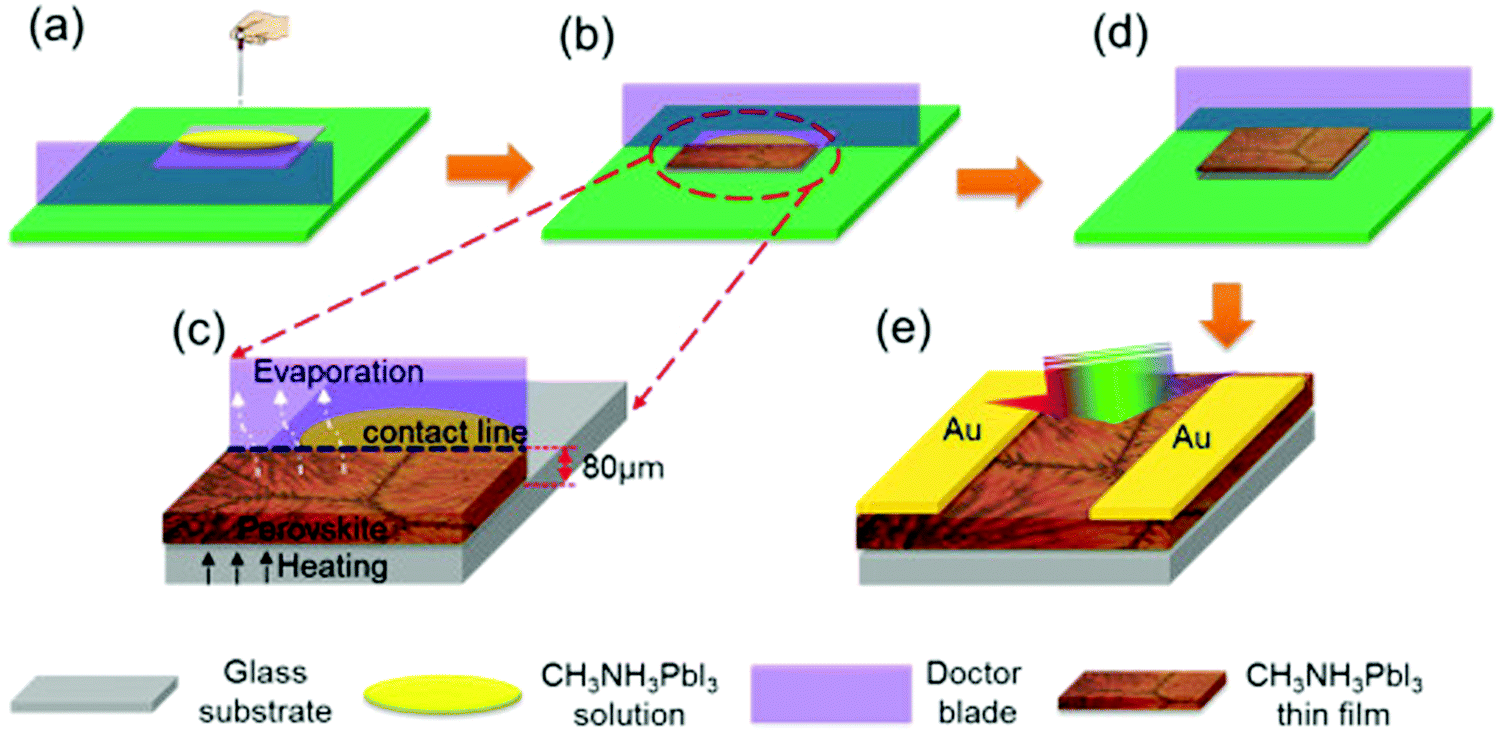 | ||
| Fig. 4 Schematic of in situ doctor blade coating technique for fabricating CH3NH3PbI3 films. (a) CH3NH3PbI3 solution (550 mg ml−1) is dropped before the doctor blade closes the substrate. (b) CH3NH3PbI3 crystal nucleate and growth during doctor blade coating. (c) Magnified schematic in (b). (d) CH3NH3PbI3 crystal film is growing with the moving of doctor blade and a large-area CH3NH3PbI3 film can be formed on the substrate. The substrate is in situ heated to 100–140 °C. The spacing between the doctor blade and the substrate is 80 μm. (e) Schematic of a CH3NH3PbI3 photodetector fabricated via doctor blade coating. The illumination light source irradiates from the front side of electrodes. Reproduced with permission from ref. 65. Copyright © 2017 Elsevier. | ||
As any other technique that has advantages and disadvantages, the blade coating technique can show some disadvantages which come from controlling the gap between the blade and the substrate. The disadvantages can be overcome by monitoring the blade geometry as well as its speed, in addition to the viscosity of the ink and the substrate wettability.
The main target to obtain either small-area PSCs or large-area PSMs is to assemble high-quality large-area perovskite layers that is secure from the doctor blade coating technique as illustrated in Fig. 4.65 To follow the procedure for film assembly via the blade coating method, a solution of appropriate concentration is added to the substrate and the doctor blade is moved at an optimized speed of 1.0 cm s−1 to form a contact line (Fig. 4a and b).65 The aggrandize structure of contact line is shown in Fig. 4c.66 By reason of the in situ thermal annealing of the substrate, the solvent evaporates very rapidly and forms the perovskite film (Fig. 4d and e).65
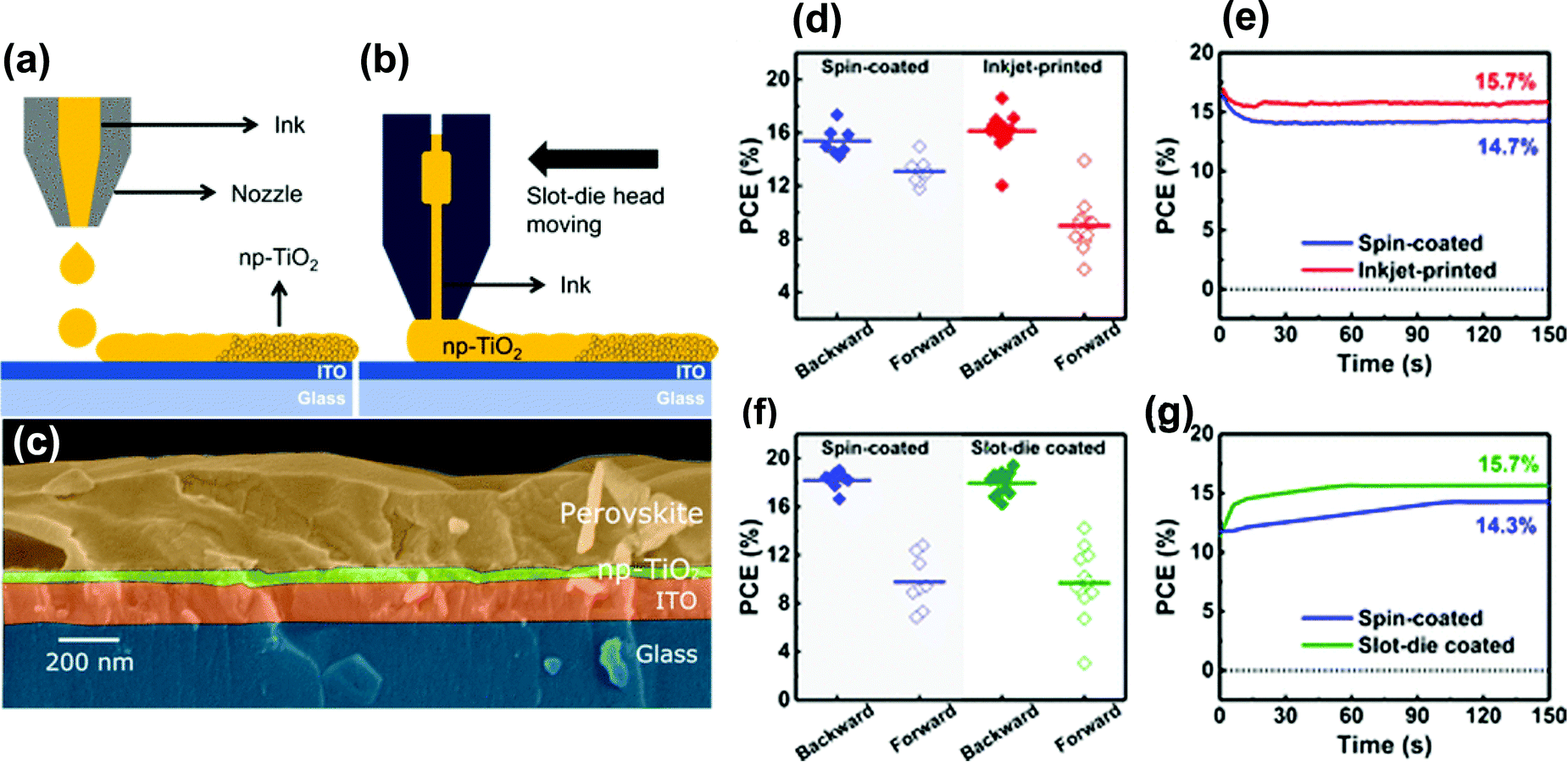 | ||
| Fig. 5 Schematic of (a) inkjet printing and (b) slot-die coating of the np-TiO2 ETL is shown with the respective power conversion efficiencies of perovskite solar cells, fabricated on top of these layers in panels (d) and (f). (c) The cross-section SEM of the assembled perovskite solar cell. PCEs measured at a constant voltage near the maximum power point under AM1.5G illumination are represented in panel (e) and MPP tracking in panel (g) for 150 s. Blue, red, and green represent PCEs of PSCs fabricated with spin-coated, inkjet-printed, and slot-die-coated np-TiO2 ETL, respectively. Reproduced with permission from ref. 76. Copyright © 2018 American Chemical Society. | ||
Comparing slot-die coating with other deposition methods like blade ones, although it need more amount of inks, which is considered as a disadvantage of that technique, it shows better yield and reproducibility for the fabricated layers with uniform surface, good morphology and crystallinity.69–71 Inkjet printing as well as slot-die is an auspicious printing pathway to develop the assembly of PSCs with a scale up range for up to 51 cm2 active area, and can be predominantly significant even for roll-to-roll manufacturing in the future.72–75 The cross-section SEM of the fabricated perovskite solar cell based on TiO2 nanoparticles, by the coating technique, is illustrated in Fig. 5c.76
Scalable fabrication of PSCs depending on TiO2 nanoparticles deposited by inkjet-printing as well as slot-die methods exhibits high PCE (measured in backward and forward directions) compared to the samples attained by the spin coating technique as shown in Fig. 5d and f. Likewise, PCE at a persistent voltage up to the maximum power point (MPP) was checked for both devices (Fig. 5e and g).72 The good results obtained for the different cells with two techniques confirm the possibility to use these techniques for large-scale fabrication and can open up a new pathway for all inkjet (or slot-die)-printed PSCs.76–79
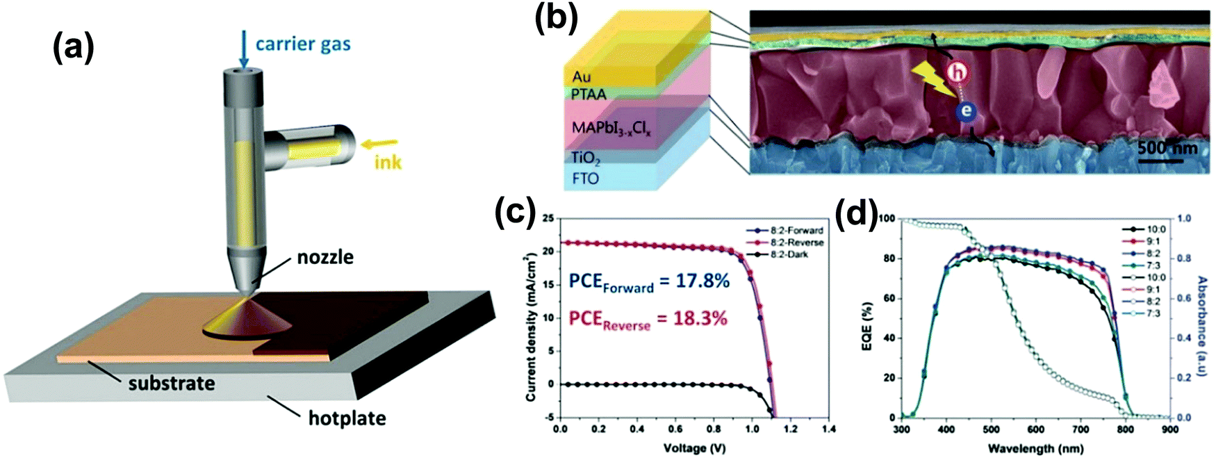 | ||
| Fig. 6 Spray coating. (a) Schematic of the spray coating process. (b) SEM cross-sectional image of a high-quality spray-coated MAPbI3−xClx perovskite absorber. (c) PCEs up to 18.3% in reverse J–V characteristics and (d) high external quantum efficiency (EQE) were achieved, which is a result of a careful solvent engineering of the spray process. Reproduced with permission from ref. 91. Copyright © 2019 WILEY-VCH. | ||
In summary, to upscale the perovskite thin-film layers, spray coating is considered as an appropriate pathway towards that achievement. Diverse parameters like precursor, solvents, nozzle spray angle, the scanning speed, and the flow rate considered as advantages of that technique should be controlled for an attainable extraordinary throughput assembly and controlling the quality of perovskite thin films.89–91
2.5. Printing techniques for perovskite photovoltaics
In addition to the different coating techniques used to assemble both perovskite solar cells and perovskite solar modules, there are several printing and pattering techniques that illustrate effective potential toward attaining cells as well as modules in a good manner. The several printing pathways are presented to pave the way for upscaling PSCs and obtain PSMs controlling the quality of perovskite films deposited above large areas with a high uniform layer with good crystallinity and morphology. In the next section, some general competing printing methodologies will be discussed to gain deep knowledge on how these techniques are used for the fabrication of PSCs and going further on the way to upscaling PSMs to accomplish the methodological necessities for industrial approach of perovskite thin-films for cells and modules.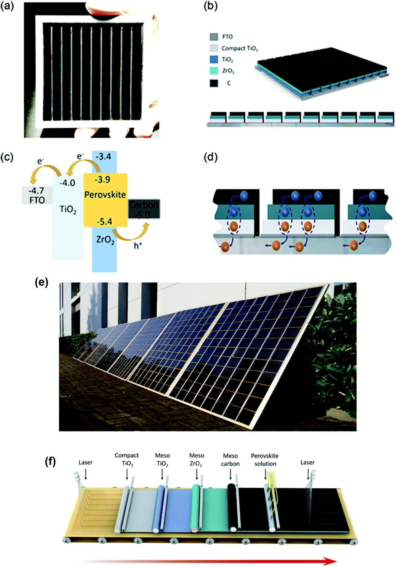 | ||
Fig. 7 (a) Image of a monolithic printable PSM with 10 subcells. (b) The monolithic interconnection scheme of the module. (c) Energy level diagrams of the hole-conductor-free printable PSC. (d) Schematic of the electron and hole separation on a serially connected PSM. (e) Image of 7![[thin space (1/6-em)]](https://www.rsc.org/images/entities/char_2009.gif) m2 printable perovskite solar panels. (f) Schematic of the proposed production line of PSMs. Reproduced with permission from ref. 98. Copyright © 2017 WILEY-VCH. m2 printable perovskite solar panels. (f) Schematic of the proposed production line of PSMs. Reproduced with permission from ref. 98. Copyright © 2017 WILEY-VCH. | ||
For the future prospects of that technique, most of the assembled devices exhibit up to 10% efficiency as well as long-term stability, which is considered as an advantage and also confirms the possibility of achieving the fully printable perovskite solar modules and put that kind of upscaling in the roadmap to efficacious commercialization of perovskite solar cells.99–101 A fully printable perovskite solar panel with 7 m2 area was fabricated as a first step in the direction of practical photovoltaic tender, as shown in Fig. 7e. Finally, each of the 1 m2 panels was accumulated via 96 PSMs and controlled modules with several numbers of sub cells. The assembled modules can be enhanced via an emerging auto production line, permitting incessant and manageable assembling process of the module (Fig. 7f).98
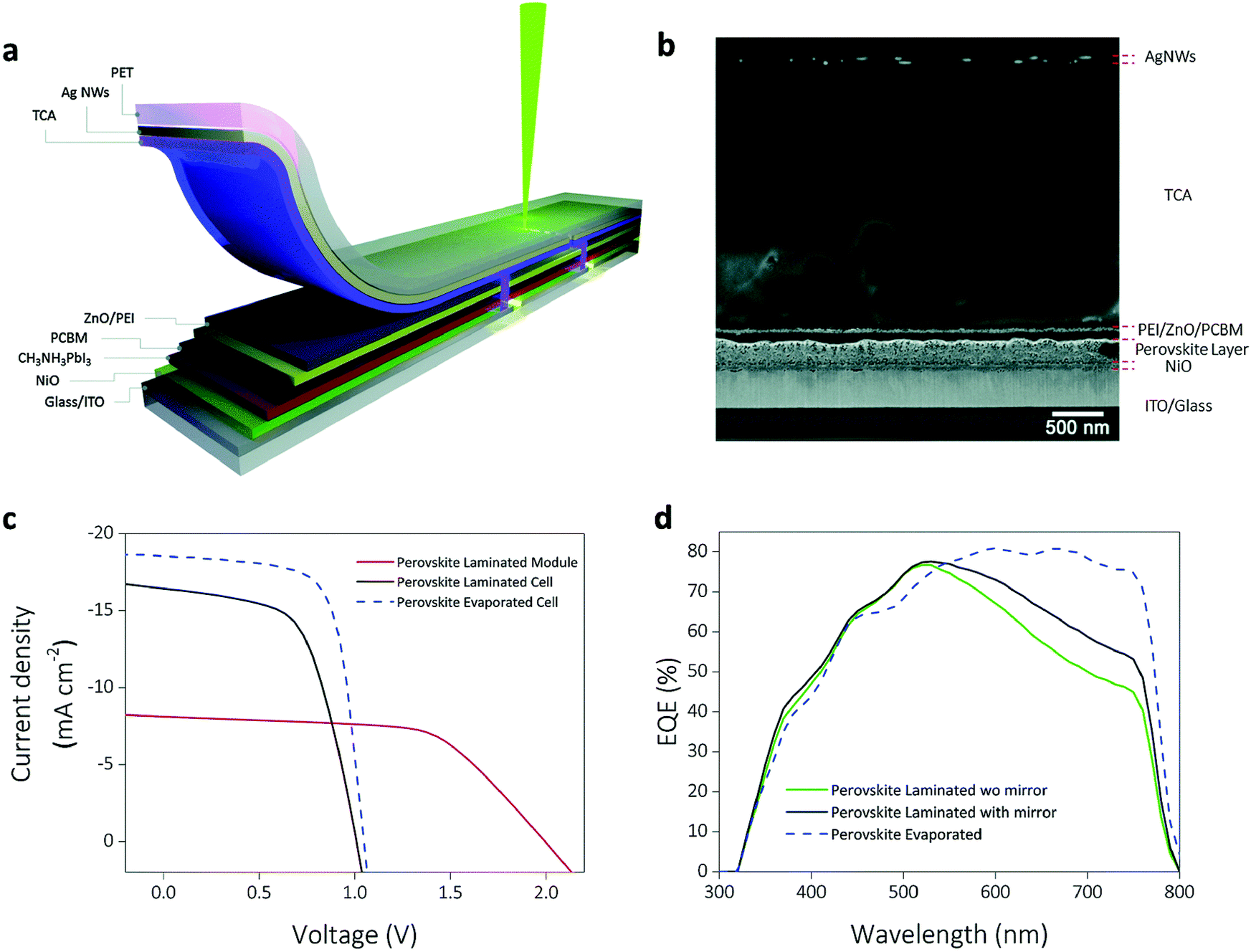 | ||
| Fig. 8 (a) Device architecture of laminated perovskite solar cell/module. (b) Cross-section scanning electron microscopic image of a laminated perovskite solar device on a glass substrate. (c) J–V characteristics of perovskite solar cells and modules with laminated top electrode. (d) EQE spectra of reference perovskite solar cell with 100 nm evaporated Ag top electrode (blue dashed line), laminated perovskite solar cells measured with reflecting mirror in the back (black line), and laminated OPV cell measured without reflecting mirror (green line). Reproduced with permission from ref. 103. Copyright © 2016 The Royal Society of Chemistry. | ||
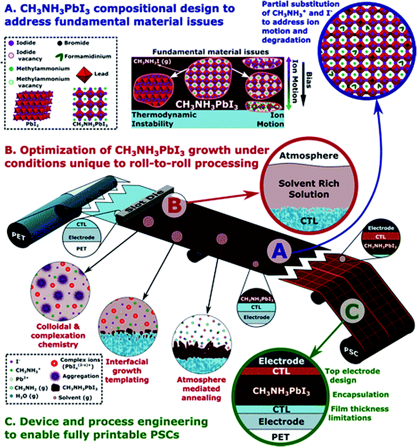 | ||
| Fig. 9 Summary of research directions necessary to fuel PSC technological translation by slot-die R2R coating. (A) Material engineering can address intrinsic ion diffusivity and degradation of CH3NH3PbI3, (B) optimization of perovskite growth under R2R conditions is necessary to reach performance requirements, and (C) device engineering is required to extend the device life and expand the material toolbox for the PSC design. Reproduced with permission from ref. 116. Copyright © 2016 American Chemical Society. | ||
Through the R2R coating pathway and to optimize the CH3NH3PbI3 growth and obtain module-scale PSCs, different parameters of perovskite compositional engineering such as the microstructure and composition are considered as essential steps in that study (Fig. 9b).116 The extreme operative approach to regulate development thus turn out to be tuning the thermodynamics driving advance over and done with precursor solution composition,117 chemistry of the surface on which progression happens,118 annealing environments, and atmosphere in the course of progress.119,120 Solution additives and solvent engineering possibly will affect the morphology and film quality, which create interface adaptation as significant contemplation in scale-up notwithstanding the challenge of film deposition by the R2R pathway.120
Furthermore, the piercing restrictions to PSC market prospective may come from thermal and ambient instabilities, which push the impending price as well as flexible PSCs to be enhanced towards the technology's existing capability intended for commercialization (Fig. 9c).116
2.6. Large-area fabrication techniques for modules
Numerous techniques such as chemical vapour deposition (CVD), vapour-assisted sequential processing and vacuum-solid reaction (VSR) considered as promising pathways compared to the other above-mentioned deposition techniques were used to fabricate solar modules with large area and long-term stability.121In order to attain perovskite modules with high efficiency and long-term stability, different parameters should be considered like the post annealing process to get homogeneous substrates with large crystals and pinhole free surface.122 Most of the vacuum deposition methods are focused to obtain different layers with promising features towards upscaling of cells in the direction of large-active-area perovskite modules.123–125
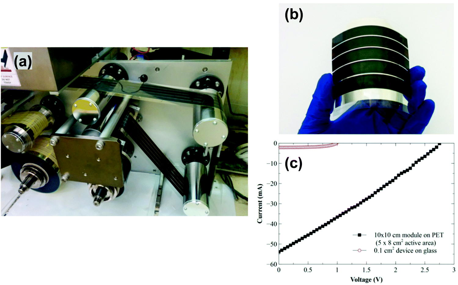 | ||
| Fig. 10 Roll-to-roll production of flexible perovskite solar cell module. (a) Roll-to-roll converted perovskite film from the cloudy PbI2 layer. (b) A photo of the printed perovskite module on a 10 cm × 10 cm substrate. The module has 5 cells in series connection and each cell has 8 cm2 of active area. (c) I–V curves of roll-to-roll printed perovskite module on ITO/PET and lab-scale-printed perovskite solar cells on ITO glass. Reproduced with permission from ref. 129. Copyright © 2015 WILEY-VCH. | ||
Additionally, a photo of the printed perovskite module on a 10 cm × 10 cm substrate is illustrated in Fig. 10b, showing that the module has 5 cells in series connection and each cell has 8 cm2 of active area. Furthermore, I–V curves of the roll-to-roll printed perovskite module on ITO/PET and lab-scale printed perovskite solar cells on an ITO glass substrate are shown in Fig. 10c.129
Furthermore, the schematic diagram in Fig. 11a illustrates the normal working distance in between the thermal sources and the rotating substrate in the evaporation system techniques that was found to be almost 20 cm.133 Regarding that distance as well as the radius of the system chamber, the thickness of the formed films will be affected and the center of the substrate will be much thicker compared to the rest of the substrate. In addition, the obtained film via deposition and after annealing can confirm through a photograph illustrated in Fig. 11b. Additionally, in order to attain both the surface roughness and surface coverage of the deposited film over an area of 5 μm × 5 μm, the atomic force microscopy (AFM) is considered as the best option to gain that important knowledge (Fig. 11c).133 The obtained data indicate that the surface roughness of the gained film is almost RRMS = 6.2 nm, which confirms the formation of homogeneous, little light scattering and very smooth layer, with no pinholes films, as checked from all the image area.133–136 The gained value for that film, obtained via a vapour deposition technique has a lower value of roughness compared to the value obtained for other materials like FAPbI3, with described roughness values ranging from 18 nm134 to above 100 nm.135 Moreover, scanning electron microscopy (SEM) as well as scanning transmission electron microscopy (STEM) is considered as a faultless tool to detect the actual morphology and give acceptable study regarding the crystal quality of the formed films for the solar cell devices. A uniform film of FAPbI3, with no observable pinholes, can be exposed from the typical cross-sectional SEM image (Fig. 11d).136–138 However, STEM was found as an important tool for observing the crystal quality and interfaces of the fabricated devices via detecting the cross-sectional images of these device. The data gained from Fig. 11e confirms the crystallites of different orientations within the perovskite film, with some extending vertically in different positions of the film. Other issues can be confirmed via the STEM image, which is the high contrast between the FAPbI3 (bright) and the carbon-rich (dark) C60 and spiro-OMeTAD that surround it.
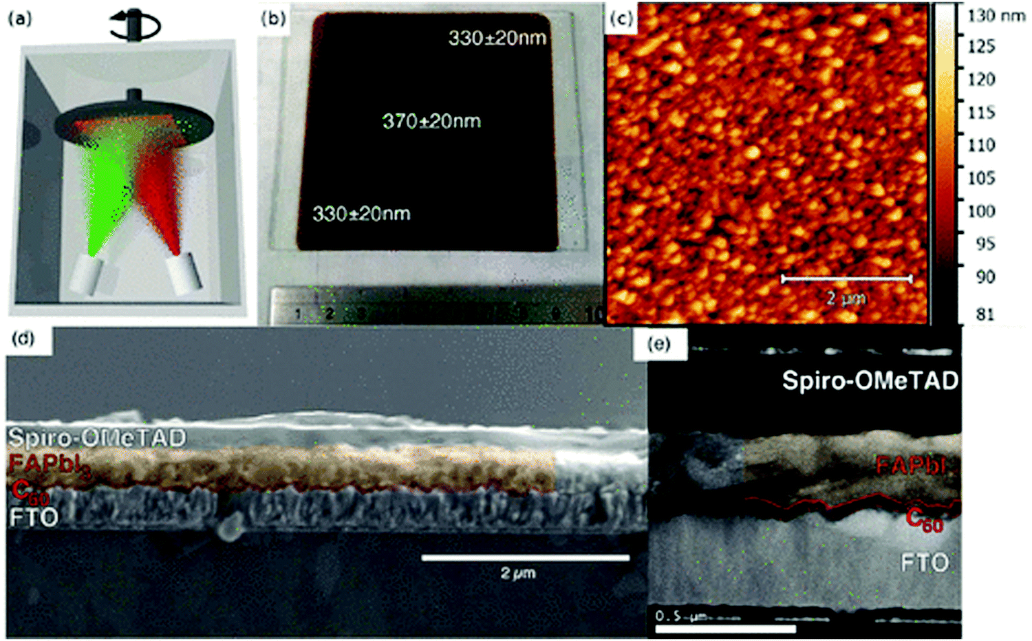 | ||
| Fig. 11 (a) Schematic of the dual-source co-evaporation system used in this study. (b) Photograph of a 8 cm × 8 cm thin film of FAPbI3 deposited on a glass substrate. The image shows the substrate after thermal annealing at 170 °C for 1 min. The results of thickness measurements at three positions are superimposed on the image, and a metal ruler with a centimetre scale is shown as a size reference. (c) Atomic force micrograph of a 5 μm × 5 μm region of the sample. The surface was found to be very smooth with a root-mean-square roughness RRMS = 6.2 nm. (d) A scanning electron microscopic image and (e) a scanning transmission electron microscopic image of a full FAPbI3 solar cell. From the bottom, the layers are a glass substrate; a fluorine-doped tin oxide (FTO) layer, a thin C60 layer, a FAPbI3 layer, a spiroOMeTAD layer, and the silver electrode. Reproduced with permission from ref. 133. Copyright © 2017 American Chemical Society. | ||
3. State-of-the-art results for modules
Compared to the state-of-the-art PCEs for spin-coated PSCs, which reached recently almost 25.2%,2 the PCEs of PSMs handled via scalable solution deposition procedures examined in the current review show less state-of-the-art records due to less optimization and control the engineering of those techniques. In Table 1, the contemporary accomplishments for coating pathways, different parameters related to the fabricated modules including perovskite structure, J–V-characteristics, solar cell area, modules area and PCEs are summarized. Intended for numerous deliberated scalable deposition methods (blade coating, slot-die coating, inkjet printing, and spray coating), the first approach was reported 5 years ago.139 However, the researchers started to focus on the upscaling of perovskite solar cells toward attaining PSMs, the enhancement of scalable solution-based deposition pathways lateness a lot if it is compared with the values of PCEs for small-area spin coating PSCs method.a
| Perovskite fabrication method | Perovskite structure | Active area (cm2) | Module area (cm2) | Number of cells inter-connected | PCEb (%) | J sc (mA cm−2) | V oc (V) | FF (%) | Ref. |
|---|---|---|---|---|---|---|---|---|---|
| a The PCE and Jsc values are provided normalized by the active area unless otherwise stated: ap, aperture area; da, designated area (active area + dead area for interconnections). CE, certified efficiency; 5-AVA, 5-aminovaleric acid. b Normalized by active area. c Stabilized PCE. | |||||||||
| Spin coating | MAPbI3 | 60 | 100 (10 × 10) | 10 | 8.7 | 1.9 | 8.1 | 57 | 140 |
| Spin coating | MAPbI3−xClx | 16.8 | 25 (5 × 5) | 5 | 5.1 | 2.0 | 4.3 | 60.3 | 141 |
| Spin coating | MAPbI3 | 40 | 100 (10 × 10) | 10 | 12.9 | 2 | 10.1 | 63.7 | 142 |
| Spin coating | CH3NH3PbI3−xClx | 10.8 | 32.5 (5.7 × 5.7) | 4 | 10.5 | 5.3 | 3.37 | 56 | 143 |
| Spin coating | CH3NH3PbI3−xClx | 7.9 | 31.4 (5.6 × 5.6) | 4 | 3.1 | 5.2 | 3.4 | 71 | 144 |
| Spin coating | MAPbI3 | 10.1 | 32.5 (5.7 × 5.7) | 4 | 13 | 4.7 | 4.2 | 66.5 | 145 |
| Spin coating | MAPbI3−xClx | 3.64 | 9 (3 × 3) | 4 | 13.6 | 19.1 | 0.9/cell | 75 | 146 |
| Spin coating | CH3NH3PbI3−x−yBrxCly | 25.2 | 100 (10 × 10) | 9 | 14.3 | 2.1 | 9.1 | 74.4 | 147 |
| Spin coating | MAPbI3−xClx | 15 (GFF ∼ 0.6) | 25 (5 × 5) | 8 | 12 | 2.6 | 8 | 58.2 | 148 |
| Spin coating | MAPbI3 | 11.25 | 25 (5 × 5) | 5 | 15.4 | 4.3 | 4.7 | 77 | 149 |
| Spin coating | MAPbI3 | 50.6 | 100 (10 × 10) | 8 | 12.6 | 2.3 | 8.6 | 64.6 | 150 |
| Spin coating | MAPbI3−xClx | 12 | 25 (5 × 5) | 3 | 11.2 | 6.5 | 2.7 | 63.8 | 151 |
| Spin coating | KxCs0.05(FA0.85MA0.15)0.92Pb(I0.85Br0.15)3 | 20 | 36 (6 × 6) | 6 | 15.6 | 3.5 | 6.8 | 65 | 152 |
| Spin coating | K0.03Cs0.05(FA0.85MA0.15)0.92Pb(I0.85Br0.15)3 | 10ap | 25 (5 × 5) | 6 | 12.4 | 3.07 | 6.5 | 62 | 153 |
| Spin coating | MAPbI3 | 22.4da | 25 (5 × 5) | 6 | 12.03 | 3.38 | 5.8 | 61.3 | 154 |
| Spin coating | [CsPbI3]0.05[(FAPbI3)0.85(MAPbBr3)0.15]0.95 | 25da | 6.5 × 6.5 | 11 | 15.3 | 1.98 | 11.2 | 0.69 | 155 |
| Bar coating | (FAPbI3)0.95(MAPbBr3)0.05 | 24.94da | 49 (7 × 7) | 8 | 17.1da | 2.72da | 8.66 | 72.6 | 156 |
| Spin coating/slot-die coating (SnO2) | Cs0.05(FA0.85MA0.15)0.95Pb(I0.85Br0.15)3 | 16.1ap | 30 (5 × 6) | 6 | 15.2 | 3.28 | 6.7 | 69 | 157 |
| Doctor blade coating | MAPbI3 | 100 | 176 (16 × 11) | 9 | 4.3 | 7.5 | 9.6 | 53.8 | 158 |
| Doctor blade coating | MAPbI3 | 11.1 | 24.2 (6.35 × 3.81) | 4 | 14.1 (13.3c) | ∼20.8 | 4.4 | ∼61.5 | 159 |
| Doctor blade coating | MAPbI3 | 33ap | 90 (6 × 15) | 17 | 15 (15.3c) | 19.5 | ∼18.2 | 72.1 | 160 |
| Slot-die coating | MAPbI3 | 40 | 100 (10 × 10) | 5 | 0.93 | 1.35 | 2.75 | 25 | 161 |
| Slot-die coating | MAPbI3 | 17.6 | 25 (5 × 5) | 8 | 10.6 | 3.25 | 6.14 | 53 | 162 |
| Slot-die coating | MAPbI3−xClx | 151.9 | 168.8 (12.5 × 13.5) | 25 | 11.1 | 17.3 | 21.2 | 67.9 | 163 |
| Screen printing | MA(5-AVA)PbI3 | 31 | 50 (5 × 10) | 4 | 10.5 | 19.6 | 3.72 | 57.5 | 164 |
| Screen printing | (5-AVA)x(MA)1−xPbI3 | 49 | 100 (10 × 10) | 10 | 10.4 | 2 | 9.3 | 56 | 165 |
| Screen printing | (5-AVA)x(MA)1−xPbI3 | 46.7 | 100 (10 × 10) | 8 | 11.2 | 2.2 | 7.1 | 70.4 | 166 |
| Screen printing | (5-AVA)x(MA)1−xPbI3 | 198 (435.6ap) | 623.7 (21 × 29.7) A4-size | 22 | 3.2 | 0.5 | 18.2 | 38.9 | 167 |
| Spray coating | MAPbI3−xClx | 40 | 100 (10 × 10) | 10 | 15.5 | 2.1 | 10.5 | 70.2 | 168 |
| Pressure processing method | MAPbI3 | 36.1ap | 64 (8 × 8) | 10 | 15.7 (12.1CE) | 2 (2CE) | 10.5 (8.36CE) | 75.7 (71.5CE) | 169 |
| HCVD | Cs0.07FA0.93PbI3 | 12 | 25 (5 × 5) | 6 | 14.6 | 3.67 | 5.84 | 0.681 | 170 |
| CVD | CsxFA1−xPbI3−yBry | 41.25 | 64 (8 × 8) | — | 12.24 | 2.25 | 9.18 | 52.8 | 171 |
| HCVD | FAPb(I0.85Br0.15)3 | 12 | 25 (5 × 5) | 6 | 14.7 | 3.55 | 6.29 | 0.66 | 172 |
| HCVD | FAPbI3 | 12 | 25 (5 × 5) | 6 | 9.0 | 2.97 | 5.64 | 0.54 | 173 |
| HCVD | MAPbI3−xClx | 15.4 | 25 (5 × 5) | 6 | 5.8 | 2.53 | 4.62 | 0.49 | 173 |
4. Perovskite solar module stability and degradation characterization
After obtaining the perovskite solar modules via different techniques and trying to improve the stability through understanding of the degradation mechanisms, it is not easy to confirm the stability and reliability of them toward the commercial attainment of perovskite photovoltaic (PV) technology.174–177 On the whole, contemporary explanations have shown the prominence of the interfaces within the device that can enhance the devices efficiency as well as stability via incorporating suitable charge-transport layers and electrode materials with appropriate compositions. Auxiliary grasp should be given to the degradation processes of perovskite modules, which have low stability issues in order to confirm the importance of the interfaces and how it can change by time.178Different techniques are suitable for characterizing the stability of module scale with large-area perovskite materials similar to the laboratory-scale to detect the features of materials at the film and device levels, also to detect the degradation at the module that is more intricate compared to small cell, as well as the interconnection features in modules.179,180
4.1. Cost, market potential and life cycle assessment of the modules
Empowering the production of solar module systems with low-cost and long-term sustainability are the current target to be achieved in order to overcome the challenged that faced the upscaling of PSCs in the direction of PSMs.181 In the literature, many research studies go forward to confirm the positive effect of lowering the fabrication cost of the perovskite modules and to reach the long-term sustainability.182–184 Nevertheless, even though these different directions tried to control the cost of the fabrication process to attain the modules, through controlling weight, structure and encapsulation of the module, the stability factor is an obstacle to continue the progress of that kind of perovskite modules.182Disablements to PSC energy grid incorporation enable the market contribution to be more probable through steady purification via these function markets. In consequence, this technology can offer superior admission toward scaling up large-area, flexible device fabrication that gain wide attention for the module market. For the research community, these current market authenticities best part fully printable PSCs and PSMs as a dynamic target intended for improvement.
Life cycle assessments are considered as an essential aspect, which concern on some of the cells and modules architectures (n–i–p structure), to confirm and detect sustainability as well as the environmental impact of PSCs and PSMs.185 It is imperative to consider the life cycle limited extent assessments that have been used in comparing PSCs with other traditional directions.
5. Challenges facing upscaling perovskite photovoltaics
Many challenges can exist while trying to upscale PSCs like the deposited materials as well as the processing techniques for fabrication, which cause depression towards large-scale positioning and may affect the device layers and the module interconnection. In fact, active area, stability as well as the cost of the proposed materials can be possible drawbacks facing the commercial upscaling of PSCs. The secrets behind the ideal device fabrication, including the amalgamations between architecture-materials to gain high performance and long-term stable devices, due to the changing in the material processing properties, still disappear that increase the existence of these challenges plainly. Besides, the active area can be affected by the series resistance of the electrodes, which resulted from the quality of configuration of the assembled layers via the coverage and uniformity, and decrease the net efficiency and stability of the invented laboratory-scale devices and modules. Moreover, the temperature, illumination and humidity may predispose the fabricated module efficiency and stability that suppose as a significant shortcoming of PSCs. By reducing both the cost and energy consumption of resource extraction including material synthesis and film processing for the different components in PSCs as well as PSMs, it will result in decreasing the cost and environmental impact of the final PV modules.6. Outlook and future perspectives
Many research directions are focused on large-scale perovskite modules to improve the fabrication techniques. However, these studies tried to optimize the ideal device architecture, but there are some drawbacks challenging the upscaling of perovskite solar cells such as the used materials, module interconnection as well as the processing challenges, including composition of perovskites. These compositions become more complex to control while conveying into the production scale and hence affect the cost of assembly, high efficiency and/or the stability of the modules. Take the price as well as environmental influence of the assembled PV modules down that will necessitate additional decreases in the cost and energy consumption of resource extraction, material preparation as well as film processing for several PSCs constituents.186–188 In addition, there are several characteristics that may enhance both the fabrication and the efficiency of the assembled modules as follows:(1) The existence of FTO substrates with high conductivity is essential to overcome the possible series resistance that may be found while assembling the solar modules. In addition to that, we should keep the optical transmittance option in order to gain all the needed features for the fabricated modules.
(2) To optimize the assembled perovskite solar module design, several parameters should be taken into account such as the deposited layers as well as the active area of the module that should be enlarged, while at the same time, the mismatch loss and internal resistance should be reduced.
(3) The improvement of the auto production line is an essential step in the upscaling process, supporting unremitting and manageable fabrication process of the module. Additionally, in order to facilitate the fabrication of perovskite modules in terawatt large-scale with reasonable cost forming and life cycle assessments, the model architecture for the fabricated devices with scalable ingredients will be recognized.188–190 To conclude, because of the extraordinary advancement for proficiency as well as long-term stability of PSCs, it is progressively necessary to think through the performance functions in the framework of scalability. It is yet precocious to understand the challenges of scaling up PSCs with reverence to the countless stacks and efficacious arrangements for module interconnection. Nonetheless, the quick progress on the way to scaling up at an appropriate performance side by side (efficiency and stability) together with the low industrialised charge competence has been previously involved in the worldwide industrial interest. The challenges for PSC scaling give a clear figure toward work requirements, which is versed by industries to ensure attaining high-efficiency and stability scalable modules.
Conflicts of interest
The author declare no conflict of interest.Acknowledgements
AES is currently on leave from CMRDI. In addition, the author appreciates the assistance of BCMaterials in Spain to follow up this study through its facilities. Furthermore, AES thanks the National Research grants from MINECO “Juan de la Cierva” [FJCI-2018-037717].References
- A. Kojima, K. Teshima, Y. Shirai and T. Miyasaka, J. Am. Chem. Soc., 2009, 131, 6050–6051 CrossRef CAS PubMed.
- National Revewable Energy Laboratory (NREL), Best Research-Cell Efficiencies, https://www.nrel.gov/pv/cell-efficiency.html, accessed: March 2020.
- A. E. Shalan, T. Oshikiri, S. Narra, M. M. Elshanawany, K. Ueno, H.-P. Wu, K. Nakamura, X. Shi, E. W.-G. Diau and H. Misawa, ACS Appl. Mater. Interfaces, 2016, 8, 33592–33600 CrossRef CAS PubMed.
- A. M. Elseman, A. E. Shalan, S. Sajid, M. M. Rashad, A. M. Hassan and M. Li, ACS Appl. Mater. Interfaces, 2018, 10, 11699–11707 CrossRef CAS PubMed.
- C. S. Ponseca Jr., T. J. Savenije, M. Abdellah, K. Zheng, A. Yartsev, T. Pascher, T. Harlang, P. Chabera, T. Pullerits, A. Stepanov, J.-P. Wolf and V. Sundstrom, J. Am. Chem. Soc., 2014, 136, 5189 CrossRef PubMed.
- K.-G. Lim, S. Ahn, Y.-H. Kim, Y. Qi and T.-W. Lee, Energy Environ. Sci., 2016, 9, 932 RSC.
- Q. Dong, Y. Fang, Y. Shao, P. Mulligan, J. Qiu, L. Cao and J. Huang, Science, 2015, 347, 967 CrossRef CAS PubMed.
- D. Shi, V. Adinolfi, R. Comin, M. J. Yuan, E. Alarousu, A. Buin, Y. Chen, S. Hoogland, A. Rothenberger, K. Katsiev, Y. Losovyj, X. Zhang, P. A. Dowben, O. F. Mohammed, E. H. Sargent and O. M. Bakr, Science, 2015, 347, 519 CrossRef CAS PubMed.
- S. D. Stranks, G. E. Eperon, G. Grancini, C. Menelaou, M. J. P. Alcocer, T. Leijtens, L. M. Herz, A. Petrozza and H. J. Snaith, Science, 2013, 342, 341 CrossRef CAS PubMed.
- G. Xing, N. Mathews, S. Sun, S. S. Lim, Y. M. Lam, M. Gratzel, S. Mhaisalkar and T. C. Sum, Science, 2013, 342, 344 CrossRef CAS PubMed.
- V. D. Innocenzo, G. Grancini, M. J. P. Alcocer, A. R. S. Kandada, S. D. Stranks, M. M. Lee, G. Lanzani, H. J. Snaith and A. Petrozza, Nat. Commun., 2014, 5, 3586 CrossRef PubMed.
- M. M. Voigt, F. Machui, L. Lucera, G. Spyropoulos, J. Cordero, P. Kubis, A. S. Ali, A. E. Shalan and C. J. Brabec, Photovoltaic Specialists Conference (PVSC), 2013 IEEE 39th, pp. 3092–3097.
- A. N. El-Shazly, A. E. Shalan, M. M. Rashad, E. A. Abdel-Aal, I. A. Ibrahim and M. F. El-Shahat, RSC Adv., 2018, 8, 24059–24067 RSC.
- A. E. Shalan and M. M. Rashad, Appl. Surf. Sci., 2013, 283, 975–981 CrossRef CAS.
- M. M. Rashad, A. E. Shalan, M. Lira-Cantu and M. S. A. Abdel-Mottaleb, J. Ind. Eng. Chem., 2013, 19, 2052–2059 CrossRef CAS.
- A. E. Shalan, M. Rasly, I. Osama, M. M. Rashad and I. A. Ibrahim, Ceram. Int., 2014, 40, 11619–11626 CrossRef CAS.
- A. E. Shalan, A. M. Elseman, M. Rasly, M. M. Moharam, M. Lira-Cantu and M. M. Rashad, RSC Adv., 2015, 5, 103095–103104 RSC.
- A. E. Shalan, M. M. Rashad, Y. Yu, M. Lira-Cantú and M. S. A. Abdel-Mottaleb, Electrochim. Acta, 2013, 89, 469–478 CrossRef CAS.
- M. M. Rashad and A. E. Shalan, Appl. Phys. A: Mater. Sci. Process., 2014, 116, 781–788 CrossRef CAS.
- E. M. Elsayed, A. E. Shalan and M. M. Rashad, J. Mater. Sci.: Mater. Electron., 2014, 25, 3412–3419 CrossRef CAS.
- A. E. Shalan, S. Narra, T. Oshikiri, K. Ueno, X. Shi, H.-P. Wu, M. M. Elshanawany, E. W.-G. Diau and H. Misawa, Sustainable Energy Fuels, 2017, 1, 1533–1540 RSC.
- A. E. Shalan, T. Oshikiri, H. Sawayanagi, K. Nakamura, K. Ueno, Q. Sun, H.-P. Wu, E. W.-G. Diau and H. Misawa, Nanoscale, 2017, 9, 1229–1236 RSC.
- A. M. Elseman, S. Sajid, A. E. Shalan, S. A. Mohamed and M. M. Rashad, Appl. Phys. A: Mater. Sci. Process., 2019, 125, 476 CrossRef.
- A. E. Shalan, S. Kazim and S. Ahmad, ChemSusChem, 2019, 12, 4116–4139 CrossRef CAS PubMed.
- A. M. Elseman, A. E. Shalan, M. M. Rashad and A. M. Hassan, Mater. Sci. Semicond. Process., 2017, 66, 176–185 CrossRef CAS.
- A. E. Shalan, A. N. El-Shazly, M. M. Rashad and N. K. Allam, Nanoscale Adv., 2019, 1, 2654–2662 RSC.
- J.-H. Im, C.-R. Lee, J.-W. Lee, S.-W. Park and N.-G. Park, Nanoscale, 2011, 3, 4088 RSC.
- Z. Li, T. R. Klein, D. H. Kim, M. J. Yang, J. J. Berry, M. F. A. M. van Hest and K. Zhu, Nat. Rev. Mater., 2018, 3, 18017 CrossRef CAS.
- J. Seo, S. Park, Y. C. Kim, N. J. Jeon, J. H. Noh, S. C. Yoon and S. I. Sang, Energy Environ. Sci., 2014, 7, 2642 RSC.
- J. H. Heo, H. J. Han, D. Kim, T. K. Ahn and S. H. Im, Energy Environ. Sci., 2015, 8, 1602 RSC.
- A. B. Djurisic, F. Z. Liu, H. W. Tam, M. K. Wong, A. Ng, C. Surya, W. Chen and Z. B. He, Prog. Quantum Electron., 2017, 53, 1 CrossRef.
- P. Cheng and X. Zhan, Chem. Soc. Rev., 2016, 45, 2544 RSC.
- F. Wang, Y. Cao, C. Chen, Q. Chen, X. Wu, X. Li, T. Qin and W. Huang, Adv. Funct. Mater., 2018, 28, 1803753 CrossRef.
- T. Bu, X. Liu, Y. Zhou, J. Yi, X. Huang, L. Luo, J. Xiao, Z. Ku, Y. Peng, F. Huang, Y.-B. Cheng and J. Zhong, Energy Environ. Sci., 2017, 10, 2509–2515 RSC.
- Y. Deng, X. Zheng, Y. Bai, Q. Wang, J. Zhao and J. Huang, Nat. Energy, 2018, 3, 560–566 CrossRef CAS.
- T. Bu, J. Li, F. Zheng, W. Chen, X. Wen, Z. Ku, Y. Peng, J. Zhong, Y.-B. Cheng and F. Huang, Nat. Commun., 2018, 9, 4609 CrossRef PubMed.
- K. Li, J. Xiao, X. Yu, T. Bu, T. Li, X. Deng, S. Liu, J. Wang, Z. Ku, J. Zhong, F. Huang, Z. Zhong, Y. Peng, W. Li and Y. Cheng, ACS Appl. Energy Mater., 2018, 1, 3565–3570 CrossRef CAS.
- F. Matteocci, S. Casaluci, S. Razza, A. Guidobaldi, T. M. Brown, A. Reale and A. Di Carlo, J. Power Sources, 2014, 246, 361 CrossRef CAS.
- F. Giordano, A. Guidobaldi, E. Petrolati, L. Vesce, R. Riccitelli, A. Reale, T. M. Brown and A. Di Carlo, Prog. Photovoltaics, 2013, 21, 1653 Search PubMed.
- H. Hoppe, M. Seeland and B. Muhsin, Sol. Energy Mater. Sol. Cells, 2012, 97, 119 CrossRef CAS.
- Y. Galagan, E. W. C. Coenen, W. Verhees and R. Andriessen, J. Mater. Chem. A, 2016, 4, 5700 RSC.
- S. Razza, S. Castro-Hermosa, A. Di Carlo and T. M. Brown, APL Mater., 2016, 4, 091508 CrossRef.
- N. J. Jeon, J. H. Noh, Y. C. Kim, W. S. Yang, S. Ryu and S. I. Seok, Nat. Mater., 2014, 13, 897–903 CrossRef CAS PubMed.
- K. Wojciechowski, S. D. Stranks, A. Abate, G. Sadoughi, A. Sadhanala, N. Kopidakis, G. Rumbles, C.-Z. Li, R. H. Friend, A. K.-Y. Jen and H. J. Snaith, ACS Nano, 2014, 8, 12701–12709 CrossRef CAS PubMed.
- Y. Hou, C. O. R. Quiroz, S. Scheiner, W. Chen, T. Stubhan, A. Hirsch, M. Halik and C. J. Brabec, Adv. Energy Mater., 2015, 5, 1501056 CrossRef.
- W. Ke, D. Zhao, C. Xiao, C. Wang, A. J. Cimaroli, C. R. Grice, M. Yang, Z. Li, C.-S. Jiang, M. Al-Jassim, K. Zhu, M. G. Kanatzidis, G. Fang and Y. Yan, J. Mater. Chem. A, 2016, 4, 14276–14283 RSC.
- Z. Ku, Y. Rong, M. Xu, T. Liu and H. Han, Sci. Rep., 2013, 3, 3132 CrossRef PubMed.
- V. Zardetto, B. L. Williams, A. Perrotta, F. Di Giacomo, M. A. Verheijen, R. Andriessen, W. M. M. Kessels and M. Creatore, Sustainable Energy Fuels, 2017, 1, 30 RSC.
- S.-J. Moon, J.-H. Yum, L. Lofgren, A. Walter, L. Sansonnens, M. Benkhaira, S. Nicolay, J. Bailat and C. Ballif, IEEE J. Photovolt., 2015, 5, 1087–1092 Search PubMed.
- M. A. Green, K. Emery, Y. Hishikawa, W. Warta and E. D. Dunlop, Prog. Photovoltaics, 2012, 20, 12–20 Search PubMed.
- L. K. Ono, N.-G. Park, K. Zhu, W. Huang and Y. Qi, ACS Energy Lett., 2017, 2, 1749–1751 CrossRef CAS.
- Z. Song, A. Abate, S. C. Watthage, G. K. Liyanage, A. B. Phillips, U. Steiner, M. Graetzel and M. J. Heben, Adv. Energy Mater., 2016, 6, 1600846 CrossRef.
- V. M. Fthenakis and P. D. Moskowitz, Prog. Photovoltaics, 2000, 8, 27–38 CAS.
- A. Babayigit, A. Ethirajan, M. Muller and B. Conings, Nat. Mater., 2016, 15, 247–251 CrossRef CAS PubMed.
- Z. Song, C. L. McElvany, A. B. Phillips, I. Celik, P. W. Krantz, S. C. Watthage, G. K. Liyanage, D. Apul and M. J. Heben, Energy Environ. Sci., 2017, 10, 1297 RSC.
- J. Seo, S. Park, Y. C. Kim, N. J. Jeon, J. H. Noh, S. C. Yoon and S. I. Seok, Energy Environ. Sci., 2014, 7, 2642–2646 RSC.
- T. Bu, X. Liu, R. Chen, Z. Liu, K. Li, W. Li, Y. Peng, Z. Ku, F. Huang, Y.-B. Cheng and J. Zhong, J. Mater. Chem. A, 2018, 6, 6319–6326 RSC.
- W. Chen, Y. Wu, Y. Yue, J. Liu, W. Zhang, X. Yang, H. Chen, E. Bi, I. Ashraful, M. Gratzel and L. Han, Science, 2015, 350, 944 CrossRef CAS PubMed.
- M. Yang, Y. Zhou, Y. Zeng, C.-S. Jiang, N. P. Padture and K. Zhu, Adv. Mater., 2015, 27, 6363 CrossRef CAS PubMed.
- W. Qiu, T. Merckx, M. Jaysankar, C. Masse de la Huerta, L. Rakocevic, W. Zhang, U. W. Paetzold, R. Gehlhaar, L. Froyen, J. Poortmans, D. Cheyns, H. J. Snaith and P. Heremans, Energy Environ. Sci., 2016, 9, 484 RSC.
- X. Li, D. Bi, C. Yi, J.-D. Décoppet, J. Luo, S. M. Zakeeruddin, A. Hagfeldt and M. Grätzel, Science, 2016, 353, 58–62 CrossRef CAS PubMed.
- A. Agresti, S. Pescetelli, A. L. Palma, A. E. Del Rio Castillo, D. Konios, G. Kakavelakis, S. Razza, L. Cina, E. Kymakis, F. Bonaccorso and A. Di Carlo, ACS Energy Lett., 2017, 2, 279–287 CrossRef CAS.
- Z. Yang, C.-C. Chueh, F. Zuo, J. H. Kim, P.-W. Liang and A. K.-Y. Jen, Adv. Energy Mater., 2015, 5, 1500328 CrossRef.
- A. T. Mallajosyula, K. Fernando, S. Bhatt, A. Singh, B. W. Alphenaar, J.-C. Blancon, W. Nie, G. Gupta and A. D. Mohite, Appl. Mater. Today, 2016, 3, 96 CrossRef.
- S. Tong, H. Wu, C. Zhang, S. Li, C. Wang, J. Shen, S. Xiao, J. He, J. Yang, J. Sun and Y. Gao, Org. Electron., 2017, 49, 347–354 CrossRef CAS.
- Y. Deng, Q. Wang, Y. Yuan and J. Huang, Mater. Horiz., 2015, 2, 578–583 RSC.
- S.-G. Li, K.-J. Jiang, M.-J. Su, X.-P. Cui, J.-H. Huang, Q.-Q. Zhang, X.-Q. Zhou, L.-M. Yang and Y.-L. Song, J. Mater. Chem. A, 2015, 3, 9092–9097 RSC.
- D. Vak, K. Hwang, A. Faulks, Y. S. Jung, N. Clark, D. Y. Kim, G. J. Wilson and S. E. Watkins, Adv. Energy Mater., 2015, 5, 1 Search PubMed.
- F. Ye, H. Chen, F. Xie, W. Tang, M. Yin, J. He, E. Bi, Y. Wang, X. Yang and L. Han, Energy Environ. Sci., 2016, 9, 2295–2301 RSC.
- W. C. Chang, D. H. Lan, K. M. Lee, X. F. Wang and C. L. Liu, ChemSusChem, 2017, 10, 1405–1412 CrossRef CAS PubMed.
- S. Das, B. Yang, G. Gu, P. C. Joshi, I. N. Ivanov, C. M. Rouleau, T. Aytug, D. B. Geohegan and K. Xiao, ACS Photonics, 2015, 2, 680–686 CrossRef CAS.
- S. Razza, S. Castro-Hermosa, A. Di Carlo and T. M. Brown, APL Mater., 2016, 4, 091508 CrossRef.
- K. Hwang, Y. S. Jung, Y. J. Heo, F. H. Scholes, S. E. Watkins, J. Subbiah, D. J. Jones, D. Y. Kim and D. Vak, Adv. Mater., 2015, 27, 1241–1247 CrossRef CAS PubMed.
- Z. Yang, C. C. Chueh, F. Zuo, J. H. Kim, P. W. Liang and A. K. Y. Jen, Adv. Energy Mater., 2015, 5, 1500328 CrossRef.
- Y. Deng, E. Peng, Y. Shao, Z. Xiao, Q. Dong and J. Huang, Energy Environ. Sci., 2015, 8, 1544–1550 RSC.
- I. M. Hossain, D. Hudry, F. Mathies, T. Abzieher, S. Moghadamzadeh, D. Rueda-Delgado, F. Schackmar, M. Bruns, R. Andriessen, T. Aernouts, F. D. Giacomo, U. Lemmer, B. S. Richards, U. W. Paetzold and A. Hadipour, ACS Appl. Energy Mater., 2019, 2, 47–58 CrossRef CAS.
- E. H. Anaraki, A. Kermanpur, L. Steier, K. Domanski, T. Matsui, W. Tress, M. Saliba, A. Abate, M. Gratzel, A. Hagfeldt and J. Correa-Baena, Energy Environ. Sci., 2016, 9, 3128–3134 RSC.
- A. Baltakesmez, M. Biber and S. Tuzemen, J. Radiat. Res. Appl. Sci., 2018, 11, 124–129 CrossRef CAS.
- J. You, L. Meng, T. Song, T. Guo, Y. M. Yang, W. Chang, Z. Hong, H. Chen, H. Zhou, Q. Chen, Y. Liu, N. De Marco and Y. Yang, Nat. Nanotechnol., 2016, 11, 75–81 CrossRef CAS PubMed.
- Z. Liang, S. Zhang, X. Xu, N. Wang, J. Wang, X. Wang, Z. Bi, G. Xu, N. Yuan and J. Ding, RSC Adv., 2015, 5, 60562–60569 RSC.
- J. H. Heo, M. H. Lee, M. H. Jang and S. H. Im, J. Mater. Chem. A, 2016, 4, 17636–17642 RSC.
- D. K. Mohamad, J. Griffin, C. Bracher, A. T. Barrows and D. G. Lidzey, Adv. Energy Mater., 2016, 6, 1600994 CrossRef.
- A. T. Barrows, A. J. Pearson, C. K. Kwak, A. D. F. Dunbar, A. R. Buckley and D. G. Lidzey, Energy Environ. Sci., 2014, 7, 2944 RSC.
- M. Ramesh, K. M. Boopathi, T. Y. Huang, Y. C. Huang, C. S. Tsao and C. W. Chu, ACS Appl. Mater. Interfaces, 2015, 7, 2359 CrossRef CAS PubMed.
- S. Das, B. Yang, G. Gu, P. C. Joshi, I. N. Ivanov, C. M. Rouleau, T. Aytug, D. B. Geohegan and K. Xiao, ACS Photonics, 2015, 2, 680 CrossRef CAS.
- X. Xia, W. Wu, H. Li, B. Zheng, Y. Xue, J. Xu, D. Zhang, C. Gao and X. Liu, RSC Adv., 2016, 6, 14792 RSC.
- H. Huang, J. Shi, L. Zhu, D. Li, Y. Luo and Q. Meng, Nano Energy, 2016, 27, 352 CrossRef CAS.
- J. H. Heo, M. H. Lee, M. H. Jang and S. H. Im, J. Mater. Chem. A, 2016, 4, 17636 RSC.
- J. E. Bishop, T. J. Routledge and D. G. Lidzey, J. Phys. Chem. Lett., 2018, 9, 1977 CrossRef CAS PubMed.
- S. Razza, S. Castro-Hermosa, A. Di Carlo and T. M. Brown, APL Mater., 2016, 4, 091508 CrossRef.
- I. A. Howard, T. Abzieher, I. M. Hossain, H. Eggers, F. Schackmar, S. Ternes, B. S. Richards, U. Lemmer and U. W. Paetzold, Adv. Mater., 2019, 31, 1806702 CrossRef PubMed.
- Y. Rong, Z. Ku, A. Mei, T. Liu, M. Xu, S. Ko, X. Li and H. Han, J. Phys. Chem. Lett., 2014, 5, 2160 CrossRef CAS PubMed.
- L. Zhang, T. Liu, L. Liu, M. Hu, Y. Yang, A. Mei and H. Han, J. Mater. Chem. A, 2015, 3, 9165 RSC.
- Z. Ku, Y. Rong, M. Xu, T. Liu and H. Han, Sci. Rep., 2013, 3, 3132 CrossRef PubMed.
- A. Mei, X. Li, L. Liu, Z. Ku, T. Liu, Y. Rong, M. Xu, M. Hu, J. Chen, Y. Yang, M. Gratzel and H. Han, Science, 2014, 345, 295 CrossRef CAS PubMed.
- Z. L. Ku, Y. G. Rong, M. Xu, T. F. Liu and H. W. Han, Sci. Rep., 2013, 3, 3132 CrossRef PubMed.
- A. Y. Mei, X. Li, L. F. Liu, Z. L. Ku, T. F. Liu, Y. G. Rong, M. Xu, M. Hu, J. Z. Chen, Y. Yang, M. Gratzel and H. W. Han, Science, 2014, 345, 295 CrossRef CAS PubMed.
- Y. Hu, S. Si, A. Mei, Y. Rong, H. Liu, X. Li and H. Han, Sol. RRL, 2017, 1, 1600019 CrossRef.
- A. Kay and M. Grätzel, Sol. Energy Mater. Sol. Cells, 1996, 44, 99 CrossRef CAS.
- S. G. Hashmi, D. Martineau, X. Li, M. Ozkan, A. Tiihonen, M. I. Dar, T. Sarikka, S. M. Zakeeruddin, J. Paltakari and P. Lund, Adv. Mater. Technol., 2016, 2, 1600183 CrossRef.
- S. Nakano, T. Matsuoka, S. Kiyama, H. Kawata, N. Nakamura, Y. Nakashima, S. Tsuda, H. Nishiwaki, M. Ohnishi and I. Nagaoka, Jpn. J. Appl. Phys., 1986, 25, 1936 CrossRef CAS.
- S. Razza, F. Di Giacomo, F. Matteocci, L. Cina, A. L. Palma, S. Casaluci, P. Cameron, A. D’Epifanio, S. Licoccia, A. Reale, T. M. Brown and A. Di Carlo, J. Power Sources, 2015, 277, 286 CrossRef CAS.
- G. D. Spyropoulos, C. O. R. Quiroz, M. Salvador, Y. Hou, N. Gasparini, P. Schweizer, J. Adams, P. Kubis, N. Li, E. Spiecker, T. Ameri, H.-J. Egelhaaf and C. J. Brabec, Energy Environ. Sci., 2016, 9, 2302–2313 RSC.
- C. O. Ramírez Quiroz, I. Levchuk, C. Bronnbauer, M. Salvador, K. Forberich, T. Heumüller, Y. Hou, P. Schweizer, E. Spiecker and C. J. Brabec, J. Mater. Chem. A, 2015, 3, 24071–24081 RSC.
- J. Xiong, B. Yang, R. Wu, C. Cao, Y. Huang, C. Liu, Z. Hu, H. Huang, Y. Gao and J. Yang, Org. Electron., 2015, 24, 106–112 CrossRef CAS.
- Y. Shao, Z. Xiao, C. Bi, Y. Yuan and J. Huang, Nat. Commun., 2014, 5 CAS.
- Q. Lin, A. Armin, R. C. R. Nagiri, P. L. Burn and P. Meredith, Nat. Photonics, 2015, 9, 106–112 CrossRef CAS.
- R. Sondergaard, M. Hosel, D. Angmo, T. T. Larsen-Olsen and F. C. Krebs, Mater. Today, 2012, 15, 36 CrossRef CAS.
- B. Susrutha, L. Giribabu and S. P. Singh, Chem. Commun., 2015, 51, 14696 RSC.
- S. A. Gevorgyan, M. V. Madsen, H. F. Dam, M. Jorgensen, C. J. Fell, K. F. Anderson, B. C. Duck, A. Mescheloff, E. A. Katz, A. Elschner, R. Roesch, H. Hoppe, M. Hermenau, M. Riede and F. C. Krebs, Sol. Energy Mater. Sol. Cells, 2013, 116, 187 CrossRef CAS.
- F. C. Krebs, T. Tromholt and M. Jorgensen, Nanoscale, 2010, 2, 873 RSC.
- R. Rosch, F. C. Krebs, D. M. Tanenbaum and H. Hoppe, Sol. Energy Mater. Sol. Cells, 2012, 97, 176 CrossRef.
- T. M. Brown, F. De Rossi, F. Di Giacomo, G. Mincuzzi, V. Zardetto, A. Reale and A. Di Carlo, J. Mater. Chem. A, 2014, 2, 10788 RSC.
- W. S. Yang, J. H. Noh, N. J. Jeon, Y. C. Kim, S. Ryu, J. Seo and S. I. Seok, Science, 2015, 348, 1234–1237 CrossRef CAS PubMed.
- Y.-Y. Zhang, S. Chen, P. Xu, H. Xiang, X.-G. Gong, A. Walsh and S. Wei, Chin. Phys. Lett., 2018, 35, 036104 CrossRef.
- S. T. Williams, A. Rajagopal, C.-C. Chueh and A. K.-Y. Jen, J. Phys. Chem. Lett., 2016, 7, 811–819 CrossRef CAS PubMed.
- S. T. Williams, F. Zuo, C.-C. Chueh, C.-Y. Liao, P.-W. Liang and A. K.-Y. Jen, ACS Nano, 2014, 8, 10640–10654 CrossRef CAS PubMed.
- Y. Li, X. Wang, S. Wu, H. Ci, H. Xu, X. Li, H. Sun, Z. Zhang, A. Cao, X. Guo and Y. Li, J. Mater. Chem. A, 2015, 3, 18847–18851 RSC.
- Q. Chen, N. De Marco, Y. Yang, T.-B. Song, C.-C. Chen, H. Zhao, Z. Hong, H. Zhou and Y. Yang, Nano Today, 2015, 10, 355–396 CrossRef CAS.
- N. K. Noel, A. Abate, S. D. Stranks, E. S. Parrott, V. M. Burlakov, A. Goriely and H. J. Snaith, ACS Nano, 2014, 8, 9815–9821 CrossRef CAS PubMed.
- Q. Chen, H. Zhou, Z. Hong, S. Luo, H.-S. Duan, H.-H. Wang, Y. Liu, G. Li and Y. Yang, J. Am. Chem. Soc., 2014, 136, 622 CrossRef CAS PubMed.
- M. R. Leyden, Y. Jiang and Y. Qi, J. Mater. Chem. A, 2016, 4, 13125 RSC.
- J. Troughton, C. Charbonneau, M. J. Carnie, M. L. Davies, D. A. Worsley and T. M. Watson, J. Mater. Chem. A, 2015, 3, 9123 RSC.
- J. Troughton, M. J. Carnie, M. L. Davies, C. Charbonneau, E. Jewell, D. A. Worsley and T. M. Watson, J. Mater. Chem. A, 2016, 4, 3471 RSC.
- S. Das, G. Gu, P. C. Joshi, B. Yang, T. Aytug, C. M. Rouleau, D. B. Geohegan and K. Xiao, J. Mater. Chem. A, 2016, 4, 9685 RSC.
- F. Di Giacomo, V. Zardetto, A. D. Epifanio, S. Pescetelli, F. Matteocci, S. Razza, A. Di Carlo, S. Licoccia, W. M. M. Kessels, M. Creatore and T. M. Brown, Adv. Energy Mater., 2015, 5, 1401808 CrossRef.
- K. Shin, J. Park and C. Lee, Thin Solid Films, 2016, 598, 95 CrossRef CAS.
- T. M. Schmidt, T. T. Larsen-Olsen, J. E. Carle, D. Angmo and F. C. Krebs, Adv. Energy Mater., 2015, 5, 1500569 CrossRef.
- K. Hwang, Y.-S. Jung, Y.-J. Heo, F. H. Scholes, S. E. Watkins, J. Subbiah, D. J. Jones, D.-Y. Kim and D. Vak, Adv. Mater., 2015, 27, 1241–1247 CrossRef CAS PubMed.
- J. Troughton, C. Charbonneau, M. J. Carnie, M. L. Davies, D. A. Worsley and T. M. Watson, J. Mater. Chem. A, 2015, 3, 9123 RSC.
- J. Troughton, M. J. Carnie, M. L. Davies, C. Charbonneau, E. Jewell, D. A. Worsley and T. M. Watson, J. Mater. Chem. A, 2016, 4, 3471 RSC.
- S. Das, G. Gu, P. C. Joshi, B. Yang, T. Aytug, C. M. Rouleau, D. B. Geohegan and K. Xiao, J. Mater. Chem. A, 2016, 4, 9685 RSC.
- J. Borchert, R. L. Milot, J. B. Patel, C. L. Davies, A. D. Wright, L. M. Maestro, H. J. Snaith, L. M. Herz and M. B. Johnston, ACS Energy Lett., 2017, 2, 2799–2804 CrossRef CAS.
- Y. Yu, C. Wang, C. R. Grice, N. Shrestha, J. Chen, D. Zhao, W. Liao, A. J. Cimaroli, P. J. Roland, R. J. Ellingson and Y. Yan, ChemSusChem, 2016, 9, 3288–3297 CrossRef CAS PubMed.
- Z. Xie, S. Sun, Y. Yan, L. Zhang, R. Hou, F. Tian and G. G. Qin, J. Phys.: Condens. Matter, 2017, 29, 245702 CrossRef PubMed.
- T. W. Crothers, R. L. Milot, J. B. Patel, E. S. Parrott, J. Schlipf, P. Muller-Buschbaum, M. B. Johnston and L. M. Herz, Nano Lett., 2017, 17, 5782–5789 CrossRef CAS PubMed.
- M. B. Johnston and L. M. Herz, Acc. Chem. Res., 2016, 49, 146–154 CrossRef CAS PubMed.
- M. Sessolo, C. Momblona, L. Gil-Escrig and H. J. Bolink, MRS Bull., 2015, 40, 660–666 CrossRef CAS.
- M. H. Zori and A. Soleimani-Gorgani, J. Eur. Ceram. Soc., 2012, 32, 4271 CrossRef.
- J. Seo, S. Park, Y. Chan Kim, N. J. Jeon, J. H. Noh, S. C. Yoon and S. I. Seok, Energy Environ. Sci., 2014, 7, 2642–2646 RSC.
- F. Matteocci, S. Razza, F. Di Giacomo, S. Casaluci, G. Mincuzzi, T. M. Brown, A. D’Epifanio, S. Licoccia and A. Di Carlo, Phys. Chem. Chem. Phys., 2014, 16, 3918–3923 RSC.
- J. H. Heo, H. J. Han, D. Kim, T. K. Ahn and S. H. Im, Energy Environ. Sci., 2015, 8, 1602–1608 RSC.
- A. Fakharuddin, F. Di Giacomo, A. L. Palma, F. Matteocci, I. Ahmed, S. Razza, A. D’Epifanio, S. Licoccia, J. Ismail, A. Di Carlo, T. M. Brown and R. Jose, ACS Nano, 2015, 9, 8420–8429 CrossRef CAS PubMed.
- F. Di Giacomo, V. Zardetto, A. D’Epifanio, S. Pescetelli, F. Matteocci, S. Razza, A. Di Carlo, S. Licoccia, W. M. M. Kessels, M. Creatore and T. M. Brown, Adv. Energy Mater., 2015, 5, 1401808 CrossRef.
- F. Matteocci, L. Cina, F. Di Giacomo, S. Razza, A. L. Palma, A. Guidobaldi, A. D’Epifanio, S. Licoccia, T. M. Brown and A. Reale, Prog. Photovoltaics, 2016, 24, 436–445 CAS.
- W. Qiu, T. Merckx, M. Jaysankar, C. Masse de la Huerta, L. Rakocevic, W. Zhang, U. W. Paetzold, R. Gehlhaar, L. Froyen, J. Poortmans, D. Cheyns, H. J. Snaith and P. Heremans, Energy Environ. Sci., 2016, 9, 484–489 RSC.
- C.-H. Chiang, J.-W. Lin and C.-G. Wu, J. Mater. Chem. A, 2016, 4, 13525–13533 RSC.
- H.-C. Liao, P. Guo, C.-P. Hsu, M. Lin, B. Wang, L. Zeng, W. Huang, C. M. M. Soe, W.-F. Su, M. J. Bedzyk, M. R. Wasielewski, A. Facchetti, R. P. H. Chang, M. G. Kanatzidis and T. J. Marks, Adv. Energy Mater., 2017, 7, 1601660 CrossRef.
- C.-H. Chiang, M. K. Nazeeruddin, M. Gratzel and C.-G. Wu, Energy Environ. Sci., 2017, 10, 808–817 RSC.
- A. Agresti, S. Pescetelli, A. L. Palma, A. E. Del Rio Castillo, D. Konios, G. Kakavelakis, S. Razza, L. Cina, E. Kymakis, F. Bonaccorso and A. Di carlo, ACS Energy Lett., 2017, 2, 279–287 CrossRef CAS.
- G. Fu, L. Hou, Y. Wang, X. Liu, J. Wang, H. Li, Y. Cui, D. Liu, X. Li and S. Yang, Sol. Energy Mater. Sol. Cells, 2017, 165, 36–44 CrossRef CAS.
- T. Bu, X. Liu, Y. Zhou, J. Yi, X. Huang, L. Luo, J. Xiao, Z. Ku, Y. Peng, F. Huang, Y.-B. Cheng and J. Zhong, Energy Environ. Sci., 2017, 10, 2509–2515 RSC.
- T. Bu, S. Shi, J. Li, Y. Liu, J. Shi, L. Chen, X. Liu, J. Qiu, Z. Ku, Y. Peng, J. Zhong, Y.-B. Cheng and F. Huang, ACS Appl. Mater. Interfaces, 2018, 10, 14922–14929 CrossRef CAS PubMed.
- L. Qiu, Z. Liu, L. K. Ono, Y. Jiang, D.-Y. Son, Z. Hawash, S. He and Y. B. Qi, Adv. Funct. Mater., 2018, 29, 1806779 CrossRef.
- G. S. Han, J. Kim, S. Bae, S. Han, Y. J. Kim, O. Y. Gong, P. Lee, M. J. Ko and H. S. Jung, ACS Energy Lett., 2019, 1845–1851 CrossRef CAS.
- E. H. Jung, N. J. Jeon, E. Y. Park, C. S. Moon, T. J. Shin, T.-Y. Yang, J. H. Noh and J. Seo, Nature, 2019, 567, 511–515 CrossRef CAS PubMed.
- T. Bu, J. Li, F. Zheng, W. Chen, X. Wen, Z. Ku, Y. Peng, J. Zhong, Y.-B. Cheng and F. Huang, Nat. Commun., 2018, 9, 4609 CrossRef PubMed.
- S. Razza, F. Di Giacomo, F. Matteocci, L. Cina, A. L. Palma, S. Casaluci, P. Cameron, A. D’Epifanio, S. Licoccia, A. Reale, T. M. Brown and A. Di Carlo, J. Power Sources, 2015, 277, 286–291 CrossRef CAS.
- M. Yang, Z. Li, M. O. Reese, O. G. Reid, D. H. Kim, S. Siol, T. R. Klein, Y. Yan, J. J. Berry, M. F. A. M. van Hest and K. Zhu, Nat. Energy, 2017, 2, 17038 CrossRef CAS.
- Y. H. Deng, X. P. Zheng, Y. Bai, Q. Wang, J. J. Zhao and J. S. Huang, Nat. Energy, 2018, 3, 560–566 CrossRef CAS.
- K. Hwang, Y.-S. Jung, Y.-J. Heo, F. H. Scholes, S. E. Watkins, J. Subbiah, D. J. Jones, D.-Y. Kim and D. Vak, Adv. Mater., 2015, 27, 1241–1247 CrossRef CAS PubMed.
- L. Cai, L. Liang, J. Wu, B. Ding, L. Gao and B. Fan, J. Semicond., 2017, 38, 014006 CrossRef.
- F. Di Giacomo, S. Shanmugam, H. Fledderus, B. J. Bruijnaers, W. J. H. Verhees, M. S. Dorenkamper, S. C. Veenstra, W. Qiu, R. Gehlhaar, T. Merckx, T. Aernouts, R. Andriessen and Y. Galagan, Sol. Energy Mater. Sol. Cells, 2018, 181, 53–59 CrossRef CAS.
- A. Priyadarshi, L. J. Haur, P. Murray, D. Fu, S. Kulkarni, G. Xing, T. C. Sum, N. Mathews and S. G. Mhaisalkar, Energy Environ. Sci., 2016, 9, 3687–3692 RSC.
- Y. Hu, S. Si, A. Mei, Y. Rong, H. Liu, X. Li and H. Han, Sol. RRL, 2017, 1, 1600019 CrossRef.
- G. Grancini, C. Roldan-Carmona, I. Zimmermann, E. Mosconi, X. Lee, D. Martineau, S. Narbey, F. Oswald, F. De Angelis, M. Graetzel and M. K. Nazeerudin, Nat. Commun., 2017, 8, 15684 CrossRef CAS PubMed.
- F. De Rossi, J. A. Baker, D. Beynon, K. E. A. Hooper, S. M. P. Meroni, D. Williams, Z. Wei, A. Yasin, C. Charbonneau, E. H. Jewell and T. M. Watson, Adv. Mater. Technol., 2018, 3, 1800156 CrossRef.
- J. H. Heo, M. H. Lee, M. H. Jang and S. H. Im, J. Mater. Chem. A, 2016, 4, 17636–17642 RSC.
- H. Chen, F. Ye, W. Tang, J. He, M. Yin, Y. Wang, F. Xie, E. Bi, X. Yang, M. Gratzel and L. Han, Nature, 2017, 550, 92–95 CrossRef CAS PubMed.
- Y. Jiang, M. R. Leyden, L. Qiu, S. Wang, L. K. Ono, Z. Wu, E. J. Juarez-Perez and Y. B. Qi, Adv. Funct. Mater., 2018, 28, 1703835 CrossRef.
- L. Luo, Y. Zhang, N. Chai, X. Deng, J. Zhong, F. Huang, Y. Peng, Z. Ku and Y.-B. Cheng, J. Mater. Chem. A, 2018, 6, 21143–21148 RSC.
- Y. Jiang, M. Remeika, Z. Hu, E. J. Juarez-Perez, L. Qiu, Z. Liu, T. Kim, L. K. Ono, D.-Y. Son, Z. Hawash, M. R. Leyden, Z. Wu, L. Meng, J. Hu and Y. Qi, Adv. Energy Mater., 2019, 9, 1803047 CrossRef.
- M. R. Leyden, Y. Jiang and Y. B. Qi, J. Mater. Chem. A, 2016, 4, 13125–13132 RSC.
- G. Niu, X. Guo and L. Wang, J. Mater. Chem. A, 2015, 3, 8970–8980 RSC.
- H. S. Kim, J. Y. Seo and N. G. Park, ChemSusChem, 2016, 9, 2528–2540 CrossRef CAS PubMed.
- T. Leijtens, K. Bush, R. Cheacharoen, R. Beal, A. Bowring and M. D. McGehee, J. Mater. Chem. A, 2017, 5, 11483–11500 RSC.
- Y. Yang and J. You, Nature, 2017, 544, 155–156 CrossRef CAS PubMed.
- J. A. Christians, P. Schulz, J. S. Tinkham, T. H. Schloemer, S. P. Harvey, B. J. T. de Villers, A. Sellinger, J. J. Berry and J. M. Luther, Nat. Energy, 2018, 3, 68–74 CrossRef CAS.
- J. Bauer, J.-M. Wagner, A. Lotnyk, H. Blumtritt, B. Lim, J. Schmidt and O. Breitenstein, Phys. Status Solidi RRL, 2009, 3, 40–42 CrossRef CAS.
- J. E. Lee, S. Bae, W. Oh, H. Park, S. M. Kim, D. Lee, J. Nam, C. B. Mo, D. Kim, J. Y. Yang, Y. Kang, H.-s. Lee and D. Kim, Prog. Photovoltaics, 2016, 24, 1035–1043 CAS.
- D. Walter, Y. Wu, T. Duong, J. Peng, L. Jiang, K. C. Fong and K. Weber, Adv. Energy Mater., 2017, 8, 1701522 CrossRef.
- Z. Song, C. L. McElvany, A. B. Phillips, I. Celik, P. W. Krantz, S. C. Watthage, G. K. Liyanage, D. Apul and M. J. Heben, Energy Environ. Sci., 2017, 10, 1297–1305 RSC.
- M. Cai, Y. Wu, H. Chen, X. Yang, Y. Qiang and L. Han, Adv. Sci., 2017, 4, 1600269 CrossRef PubMed.
- N. L. Chang, A. W. Y. Ho-Baillie, P. A. Basore, T. L. Young, R. Evans and R. J. Egan, Prog. Photovoltaics, 2017, 25, 390–405 Search PubMed.
- J. Gong, S. B. Darling and F. You, Energy Environ. Sci., 2015, 8, 1953–1968 RSC.
- M. Kaltenbrunner, G. Adam, E. D. Głowacki, M. Drack, R. Schwödiauer, L. Leonat, D. H. Apaydin, H. Groiss, M. C. Scharber, M. S. White, N. S. Sariciftci and S. Bauer, Nat. Mater., 2015, 14, 1032–1039 CrossRef CAS PubMed.
- Y. Zhao, A. M. Nardes and K. Zhu, Appl. Phys. Lett., 2014, 104, 213906 CrossRef.
- Y. J. Liou, P. T. Hsiao, L. C. Chen, Y. Y. Chu and H. Teng, J. Phys. Chem. C, 2011, 115, 25580–25589 CrossRef CAS.
- X. Wang, Z. Lia, W. Xu, S. A. Kulkarni, S. K. Batabyal, S. Zhang, A. Cao and L. H. Wong, Nano Energy, 2015, 11, 728–735 CrossRef CAS.
- Y. Wu, X. Yang, W. Chen, Y. Yue, M. Cai, F. Xie, E. Bi, A. Islam and L. Han, Nat. Energy, 2016, 1, 16148 CrossRef CAS.
| This journal is © The Royal Society of Chemistry 2020 |