
 Open Access Article
 This Open Access Article is licensed under a
 Creative Commons Attribution 3.0 Unported Licence
Defining the plasmonic cavity performance based on mode transitions to realize highly efficient device design†
Vasanthan
Devaraj
 a,
Jong-Min
Lee
a,
Donghan
Lee
*b and
Jin-Woo
Oh
*ac
a,
Jong-Min
Lee
a,
Donghan
Lee
*b and
Jin-Woo
Oh
*ac
aResearch Center for Energy Convergence and Technology Division, Pusan National University, Busan 46241, South Korea. E-mail: ojw@pusan.ac.kr
bDepartment of Physics, Chungnam National University, Daejeon 34134, South Korea. E-mail: dleee@cnu.ac.kr
cDepartment of Nanoenergy Engineering, Pusan National University, Busan 46241, South Korea
First published on 22nd April 2020
Abstract
Designing and realizing high-potential applications in the fields of energy conversion, fuel generation, sensors, and photonic devices require a precise understanding of fundamental plasmonic properties. In the above-mentioned applications, a plasmonic nanoparticle on mirror (NPOM) nanostructure is employed as one of the key fundamental components. However, NPOM's plasmonic properties are not understood in detail, especially in terms of mode transitions along with the edge effect, which is a crucial requisite in devising device efficiency. In this work, we classified the plasmonic nanocavity strength and its respective near-field enhancement deterioration rate% based on mode transitions and the edge effect, which plays a significant role in defining the device efficiency. Superior light properties with a slower near field enhancement deterioration rate% (55%) from the NPOM nanostructure can be observed when it exhibited an unchanged dipolar mode (in the high plasmonic nanocavity strength region) in combination with the edge effect (medium to NP-only strength region). In the case of the quadrupolar to dipolar mode transition, two interesting cases of surface charge evolution are reported: case one – smaller near-field enhancement numbers are obtained when the NP surface charge close to the metallic mirror disappears during the mode transition; and case two – higher near-field enhancement numbers are obtained when the NP surface charge close to the metallic mirror dominates during the mode transition. Irrespective of both scenarios, the quadrupolar to dipolar mode transition resulted in a rapid near field enhancement deterioration rate% (case one – 86%, case two – 81%). We find that the NPOM nanostructure with a combination of an unchanged dipolar mode and edge effect property can uplift the efficiency of devices in multiple applications.
Introduction
In recent years, plasmonics has attracted potential interest for use in highly efficient devices in the fields of energy conversion, fuel generation, sensors, and photonic devices.1–14 Understanding plasmonic mode fundamentals and properties is critical, as these factors play a defining role in material performance.15–21 Factors like flexibility and simplicity in fabrication, good geometrical tolerance, large dielectric layer thicknesses with superior device characteristics, and low-cost processing are essential for developing next-generation devices with multiple applications.22–29 Significantly, the nanoparticle shape, material, design, and size in a plasmonic device play considerable roles in determining the localized surface plasmon resonance (LSPR) and near-field enhancement properties.30–36 In addition to these parameters, it is necessary to consider the geometrical edge effect, which influences the near field enhancement in plasmonic nanostructures. In applications reported dominantly utilizing plasmonic nanoparticles (NPs), the presence of compounds, molecules or quantum dots is dominantly seen close to edges of the NPs. It is essential to consider the edge effect, which determines the efficiency of the device. For this purpose, considering the plasmonic modes and their transitions under various conditions is indispensable.The origins of plasmonic modes (dipole, quadrupole, and other higher-order modes) and mode transitions in the presence of geometrical modifications are important for determining device properties (e.g., the light coupling efficiency, light confinement, extraction, and absorption).16–18,20,30,36,37 These mode properties define the plasmonic nanocavity strength and light confinement probability based on geometric tolerances. Superior light confinement at sub-wavelength scales and the deterioration of near-field enhancement are primarily defined by these plasmonic modes and their modifications under various geometric conditions. The combination of plasmonic modes and geometrical edge effects will play a critical role in improving device properties such as absorption, field enhancement, and power conversion efficiencies. These properties are fundamental to realizing highly efficient devices in the fields of energy conversion, chemical/biological sensors, cavity quantum electrodynamics, surface-enhanced spectroscopies, single molecule detection, and waveguiding.4,7,9,11,19,27,35–43 The importance of the above-mentioned plasmonic modes is illustrated by plasmonic nanoparticle–film coupled systems, commonly referred to as nanoparticle (NP) on mirror or NPOM systems. These systems display rich plasmonic modes and have a high potential technological utility.11,16,19,27,35,41,44,45 These NPOM designs mimic theoretical free-space dimer (FSD) designs, in which two metallic nanoparticles (NPs) are separated by a nanogap distance to create a hot spot.36,44,45 The dielectric layer inserted between the NP and mirror acts as a virtual hot-spot region, in which attractive plasmonic properties can be realized.
In this work, we would like to investigate the primary importance of plasmonic modes (non-transition and transition modes) in combination with the edge effect upon geometric variation and their influence on: (i) the strength of the plasmonic nanocavity, and (ii) the near-field enhancement deterioration rate based upon the combination of plasmonic mode transitions and the edge effect. Instead of discussing which NP shape provides superior plasmonic characteristics, we systematically studied the plasmonic nanocavity strength, from high to low strengths, the near-field enhancement, the edge effect, and the origin of the modes underlying this trend. Similarities and differences between the plasmonic nanocavity strengths were thoroughly investigated. The in-depth analysis of plasmonic modes in combination with the edge effect reported here will help provide interesting insights for applications in multiple fields.
Materials and methods
Modeling
A schematic diagram (Fig. 1a) of the plasmonic nanostructure (NPOM) surrounded by air was investigated using three-dimensional (3D) finite element method (FEM) simulations (COMSOL Multiphysics 5.5, Waveoptics Module). NPOM nanostructures having common NP shapes (sphere, disk, and cube) were used to assess the plasmonic nanocavity functionality. To simplify the work, the NP diameter was fixed to 80 nm throughout our simulations. The cube was modeled as having rounded corners, with a radius of curvature of 8 nm, as described previously.11,41 The disk thickness was fixed to 30 nm. The near-field enhancement numbers for a disk with t = 2 nm and a cube were comparable. To avoid complex quantum effects in NPOM, we started with t ≥ 2 nm.45,46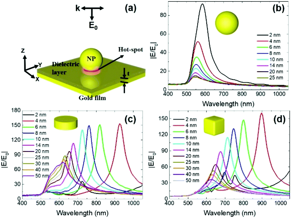 | ||
| Fig. 1 (a) Three-dimensional schematic diagram of the NPOM plasmonic structure with broadband plane wave light source excitation applied from the top. NPs with shapes of a sphere, disk, or cube, and their optical properties are discussed and compared in detail. Simulated broadband near-field enhancement |E/E0| results obtained from the following NP shapes in the NPOM nanostructure: (b) sphere, (c) disk, and (d) cube. Various simulations were carried out as a function of the dielectric layer thickness t (minimum of 2 nm and maximum of 50 nm). | ||
The dielectric layer (refractive index n = 1.5) thickness t was varied from 2 nm to 50 nm. The NP and metallic mirror material properties were assigned to the values for gold. The refractive index of gold was taken from the Johnson and Christy database and was modeled using Lorentz–Drude dispersion fitting.44–48
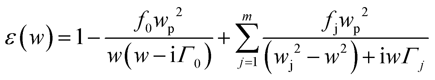 | (1) |
The material index fitting from eqn (1) is divided into two: the first term describes Drude fitting with plasma frequency “wp”, oscillator strength “f0”, and damping constant “Γ0”; the second term being the Lorentz modification describing the number of oscillations “m” with frequency “wj”, oscillator strength “fj”, and damping constant “Γj”. A broadband plane wave source was used to excite the NPOM nanostructure from the top (+Z direction).
Near-field enhancement calculation
The refractive index of gold was taken from the Johnson and Christy database and was modeled using Lorentz–Drude dispersion fitting.44–47 A broadband plane wave source was used to excite the NPOM nanostructure from the top (+Z direction). The broadband near-field enhancement |E/E0| was extracted using a box-shaped electric field monitor closely surrounding the NPOM nanostructure. The average volume integral of |E/E0| was obtained from the average near-field enhancement spectroscopy as follows:17,36,44,45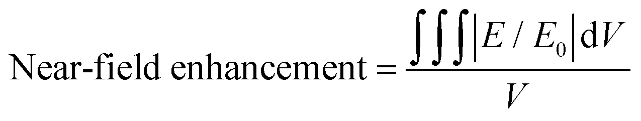 | (2) |
In eqn (2), E describes the local electric field (Ex, Ey, Ez), the amplitude of the incident electric field is E0, and V is the volume at a certain distance within the metal film–NP surface.
Three-dimensional surface charge mapping
The skin effect and integration of Gauss's law were used to calculate the surface charge density (ρ).17,21,37,44 A large induced charge density (ρr) was assumed to be present at the surface (S) of the metal, and this density decreased exponentially as it spread within the metal as per the skin effect.| ρr = ρe−r/δ | (3) |
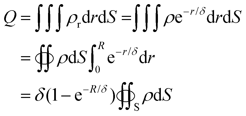 | (4) |
 | (5) |
 | (6) |
Results and discussion
Broadband near-field enhancement spectra
The simulated NPOM designs prepared from three different NP shapes (cube, disk, and sphere) are shown in Fig. 1a. (The model is discussed in detail in the Materials and methods section.) These three NPs are primarily chosen here for two significant reasons: commercial availability of NPs or more facile fabrication compared to other NPs by lithography; and most studied and reported for device applications. Broadband near-field enhancement |E/E0| spectra of the three NP shapes used in the NPOM design are shown in Fig. (1b–d). Of all the NP shapes, the sphere-based NPOM design displayed extreme sensitivity to |E/E0| as a function of the dielectric layer thickness (Fig. 1b). The |E/E0| numbers rapidly dropped as the dielectric layer thickness increased from 2 nm to 10 nm, with minimal differences in the resonance |E/E0| wavelength λ shift as compared with the disk- or cube-based NPOM nanostructures. The other NP shapes (Fig. 1c and d) indicated that the resonance |E/E0| wavelength (λ) was indicated by a ∼1.7-fold increase in the |E/E0| strength. Please see the ESI,† Fig. S2, for the disk- and cube-based NPOM plasmonic nanostructures’ broadband near-field enhancement |E/E0| results for the t = 2 nm condition (at wavelengths between 1000 nm and 1300 nm).The plasmonic nanocavity effects obtained from the simulated NPOM designs were explored by extracting and plotting the resonance |E/E0| wavelength λ (Fig. 2a) and its maximum |E/E0| (Fig. 2b) as a function of the dielectric layer thickness t. As discussed earlier, the sphere-based NPOM nanostructure displayed poor plasmonic characteristics compared with the other NP shapes. Note that the plasmonic nanocavity region in the sphere-based NPOM design mimicked a point-shaped cavity (NP–film interface, as shown in the XY cross-section). This point-shaped contact formed a smaller plasmonic nanocavity volume (or hot-spot region). Hence, severe deterioration in the near-field enhancement was noted, even with minimal dielectric layer thickness modification. Note that this NPOM plasmonic nanocavity mimics a metal–insulator–metal (MIM) structure in which the resonance wavelength tuning depended on the cavity width of the structure.44 The MIM approximation attributed the minimal difference in the resonance |E/E0| wavelength λ shift (36 nm) to the sphere-based NPOM's smaller cavity width (λ shifted from 585 nm to 549 nm as t varied from 2 nm to 10 nm), in contrast with the disk and cube NPOM designs. For t > 10 nm, no major changes in the sphere-based NPOM design were observed.
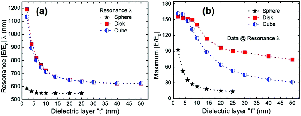 | ||
| Fig. 2 Resonance |E/E0| wavelength λ (a) and respective maximum near-field enhancement |E/E0| (b) data as a function of the dielectric layer thickness for the sphere-, disk-, and cube-based NPOM plasmonic nanostructures. These numbers were extracted from the broadband spectra presented in Fig. 1. The dashed lines are provided as a guide to the eye. | ||
Interestingly, the disk- and cube-based NPOM nanostructures followed a similar trend in the resonance |E/E0| wavelength λ modification when t was varied from 2 nm to 50 nm. Thin dielectric layer variations (between 2 nm and 10 nm) revealed the following differences in the resonance |E/E0| wavelength λ shift: 469 nm broadband tuning for the disk (1192 nm to 723 nm) and 423 nm broadband tuning for the cube (from 1135 nm to 712 nm). For t > 10 nm, the difference in the resonance |E/E0| wavelength λ modification was small: 54 nm (disk) and 51 nm (cube). By contrast, major differences in the near-field enhancement were observed in the cube- and disk-based NPOM plasmonic nanostructures. The near-field enhancement trends could be divided into two cases: case one, encompassing t variations between 2 nm and 20 nm, and case two, encompassing t variations >20 nm. At t = 2 nm, the extracted maximum near-field enhancement numbers were similar for the disk = 156 and cube = 161 nanostructures. The disk-based design's |E/E0| deteriorated by 59 over the case one range (at t = 20 nm, the near-field enhancement was 97) and the value for the cube deteriorated by 98 (at t = 20 nm, the near-field enhancement was 64). Rapid near-field enhancement deterioration was clearly observed for the cube-based NPOM over the case one range. A similar trend in |E/E0| deterioration was observed over the case two range for both plasmonic nanocavity designs, with a decrease of 21 for the cube (at t = 50 nm, the near-field enhancement was 31) and a decrease of 23 for the disk (at t = 50 nm, the near-field enhancement was 74). The disk-based NPOM nanostructures exhibited superior optical characteristics as t increased. Note that the longer wavelength resonance condition for the cube- and disk-based NPOMs with a thin dielectric layer arose from the wide plasmonic cavity relative to that formed by the sphere-based NPOMs, which mimicked the MIM structure.47
Classification of the plasmonic nanocavity strength
Considering the |E/E0| resonance wavelength shift and its respective near-field enhancement properties as a function of t, we classified the NPOM design plasmonic nanocavity strengths (Fig. 3a). The Fig. 2 results were used to divide the plasmonic nanocavity strength into three categories: (i) strong; (ii) medium-to-low; and (iii) NP-only. The third classification, NP-only, indicated that the contribution to the near-field enhancement arose only from the NP, and the hot spot or t contributions were negligible. The plasmonic nanocavity strengths as a function of the dielectric layer t were as follows (listed in the order of high; medium-to-low; and NP-only): sphere NPOM (≤6 nm; >6 to 10 nm; >10 nm), and disk and cube NPOMs (≤14 nm; >14 to 35 nm; >35 nm). These properties were reflected in the three-dimensional electric field amplitude profiles (Fig. 4), which identified the contributions of the near-field enhancement regions. The ESI,† Fig. S3, shows the conventional cross-sectional XZ electric field amplitude profiles. In addition to larger “hot-spot” volume, the edge-based near field enhancement influence can be observed for disk- and cube-based NPOM nanostructures, which resulted in better |E/E0| numbers (for both similar and higher t conditions) when compared with the spherical NP. This edge effect is critical for NPOM based device applications utilizing the mixing of compounds, molecules or quantum dots as a high probability of attachment was seen with edge(s).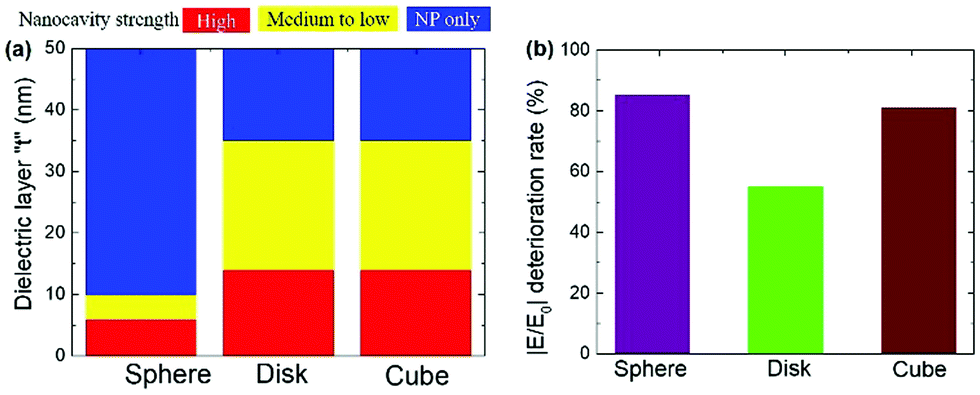 | ||
| Fig. 3 (a) Classification of the plasmonic nanocavity strength in the NPOM nanostructures prepared with sphere-, disk-, and cube-shaped NPs as a function of the dielectric layer thickness. (b) Near-field enhancement deterioration rate percentage, which emphasizes the importance of the NP shapes studied in this work. | ||
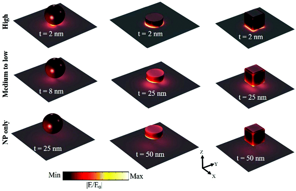 | ||
| Fig. 4 Three-dimensional electric field amplitude profiles for the sphere-, disk-, and cube-based NPOM plasmonic nanostructures extracted from different classifications of the plasmonic nanocavity strength, as described in Fig. 3. | ||
Near-field enhancement deterioration rate%
We next compared the deterioration of the near-field enhancements for the NPOM nanostructures employed in this work. The |E/E0| deterioration rate% was calculated using the data presented in Fig. 2b. The minimum to highest ratio of the |E/E0| difference provided the deterioration rate% (see the ESI† for details). The calculated |E/E0| deterioration rate% values are shown in Fig. 3b. Deterioration rates of 85%, 55%, and 81% were observed for the sphere-, disk-, and cube-based designs, respectively.It is necessary to understand why the near-field enhancement in the cube-based nanostructures deteriorated rapidly despite having a nanocavity strength classification (along with the edge effect) similar to that of the disk NPOM. In addition, we considered why the |E/E0| deterioration rate% trends for the cube and sphere NPOMs were similar. The electric field amplitude profiles alone did not provide answers to these questions; therefore, we utilized the three-dimensional surface charge distribution mappings (explained in Section 2.3), which offered an interpretation of this complex phenomenon (Fig. 5).
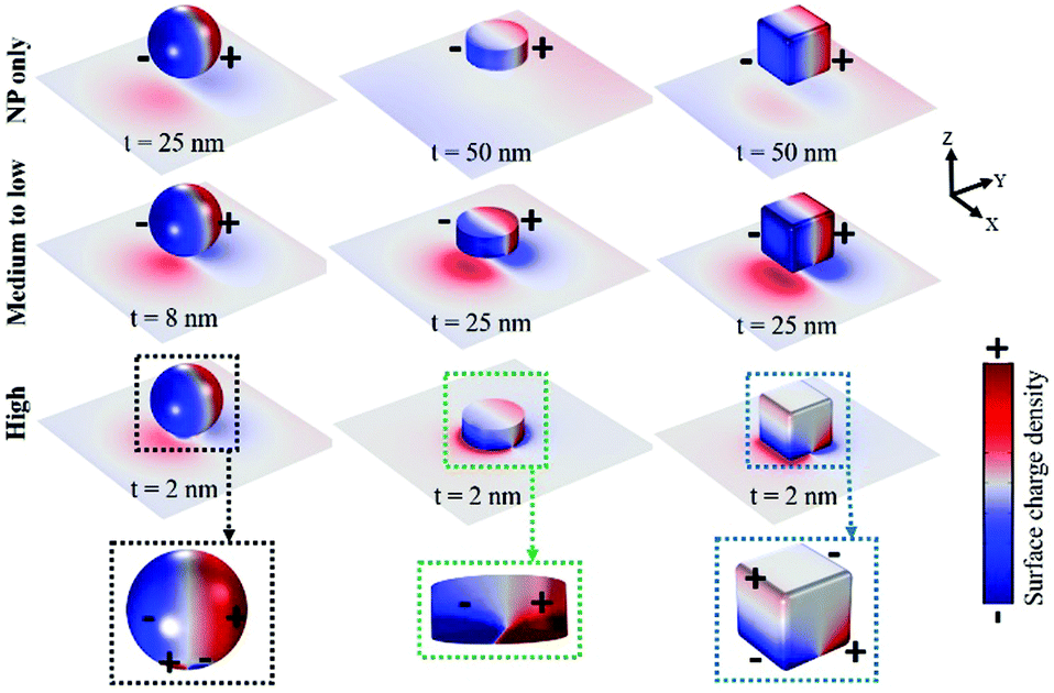 | ||
| Fig. 5 Three-dimensional surface charge density mappings for the sphere-, disk-, and cube-based NPOM plasmonic nanostructures based on three primary classifications of the plasmonic nanocavity strength, as described in Fig. 3. The highlighted colored dashed boxes show the available modes in the nanoparticle when the plasmonic nanocavity strength is high. The illustration of positive and negative charge signs is marked only for NPs to clarify the interpretation of the results (for the film case, the charge signs are not marked). | ||
Mode transitions
As mentioned in the introduction, rather than discussing which NP shape is best, it is significant to view the influence of near field enhancement in terms of plasmonic mode transitions concerning t modification in the NPOM nanostructure. Based on the three-dimensional surface charge density mappings of the simulated NPOM nanostructures (Fig. 5), we primarily categorize the mode transitions (from “high” → “medium-to-low” nanocavity strength region) into two types: type one → dipolar mode only (ex. disk NPOM) and type two → quadrupolar to dipolar mode transition (ex. sphere and cube NPOM). In the type one category, irrespective of t modification, the dipolar mode remains unchanged. This dipolar mode only disk NPOM's optical property reveals its superior near field enhancement properties when compared to the other designs presented in this work. Coming to the type two category, it is interesting to see a significant difference in the sphere and cube as to how the quadrupolar mode changes to the dipolar mode with an increase in the dielectric layer thickness: sphere NPOM → disappearance of bottom surface charges in the NP; cube NPOM → disappearance of the top (Fig. 6). In the sphere NPOM's quadrupolar mode condition (t = 2 nm), the dominance of surface charges in the NP close to the metallic mirror (bottom part) becomes less when compared to the top part. As t increases, the bottom part's surface charges become negligible and disappear. In other words, the surface charges covering the sphere NP's top part dominate the entire NP region when it changes to the dipolar mode. Looking at a similar condition with the cube NPOM's quadrupolar mode (t = 2 nm), it is the opposite case to the sphere. The contribution of surface charges in the bottom part of the cubic NP close to the metallic mirror becomes dominant and completely covers the NP when it changes to the dipolar mode (in other words, the surface charges covering the top part of the NP disappear). This fundamental change in the NP's surface charge property explains the better performance for the cube when compared with the sphere despite having a similar quadrupolar to dipolar mode transition. Higher |E/E0| numbers can be obtained from the NPOM nanostructure if the NP's bottom part surface charges become dominant when changing from the quadrupolar to the dipolar mode, as seen with the cube. If the scenario becomes the reverse (surface charge dominance based upon the NP's top part, as seen with a sphere), smaller |E/E0| numbers will be obtained in comparison. However, irrespective of any case of a quadrupolar to dipolar mode transition, it will lead to a rapid |E/E0| deterioration rate%. Additionally, its possible to extract better |E/E0| (nanocavity region covering medium-to-low → NP-only) on the basis of the edge effect.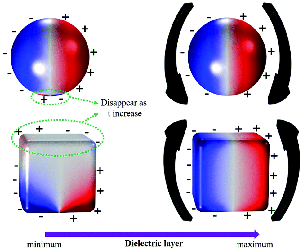 | ||
| Fig. 6 Two different cases of quadrupolar to dipolar mode transition mechanisms as a function of dielectric layer thickness modification explaining the sphere- and cube-based NPOM's optical property differences. | ||
Overall, a superior near field enhancement property is possible with the NPOM nanostructure on the basis of a combination of two factors, which results in a slower |E/E0| deterioration rate%: an unchangeable dipolar mode and the edge effect. In addition to the |E/E0| deterioration rate% obtained from the resonance |E/E0| wavelength position (or λR), we also considered the λR ± 100 nm broadband range either for wavelength-tunable applications or for material (ex. QD) resonance wavelength mismatch (especially for the cube- and disk- NPOM, see the ESI,† Fig. S4). It is necessary to design a device with excellent optical characteristics across a broad wavelength range without severe deterioration in its efficiency in spite of having minor topology defects or fabrication errors.26 Excellent optical characteristics can be seen with the disk due to its slower |E/E0| deterioration rate% all across the λR ± 100 nm range when compared with the cube. Considering all the above properties, the NPOM nanostructure involving the disk NP can boost the variety of the device performance.
Numerous studies of NPOM nanostructures have examined sphere-, disk-, and cube-based NPs. The plasmonic nanocavity strength and respective near-field enhancement deterioration rate% as a function of the mode transition and edge effect reported in this work will find significant importance. It is critical to consider the mode transition properties when designing NPOMs, as the plasmonic properties play a crucial fundamental role in the device components used for fuel generation, energy conversion, photodetectors, sensors, single-molecule detection, and photonic devices. A limited decline in device efficiency can be realized with a precise design choice of plasmonic nanostructures in terms of near-field enhancement deterioration rate%, absorption, and unchanged dipolar mode properties.49 It is crucial to note that an NPOM nanostructure having geometrical parameters delivering a non-transition mode (dipolar mode only) property in combination with the edge effect is essential to realize a highly efficient device. Note that the non-transition (dipolar) mode-based NPOM nanostructures support a flexible geometrical tolerance that is advantageous for device fabrication due to an unchangeable dipolar mode property. On the other hand, NPOM nanostructures that support transition modes (quadrupolar to dipolar) display poor plasmonic characteristics because these mode changes limit the device functionality. It is possible to realize a highly efficient device based upon the cube NPOM but that comes with a restriction (only at thinner t). In short, NPOM nanostructures with non-transition modes achieve superior geometrical tolerance, enabling low-cost device fabrication.
Conclusions
In summary, we presented a three-dimensional FEM simulation study of NPOM plasmonic nanostructures based on three commonly used NP geometries: sphere, disk, and cube. We designed a measure to assess the plasmonic nanocavity strength and respective near-field enhancement deterioration rate% on the basis of mode transitions and the edge effect. Better plasmonic nanocavity strengths were observed using the disk and cube NPOMs compared with the sphere NPOM. The near-field enhancement deterioration rate% showed a superior optical performance for the disk (versus cube) NPOM, despite having similar plasmonic nanocavity strength classifications. The superior light confinement and enhancement properties of the disk NPOM were attributed to the non-transition mode (dipolar mode only) behavior in combination with the edge effect. Rapid deterioration in |E/E0| was observed using the cube and sphere NPOMs due to the transition mode (quadrupolar-to-dipolar). A non-transition dipolar mode-based NPOM design in combination with the edge effect has high technological potential because it can be used to fabricate highly efficient devices for use in multiple fields with flexible fabrication specifications and good broadband usage.Conflicts of interest
The authors declare no conflicts of interest.Acknowledgements
This work was supported by the Creative Materials Discovery program of the National Research Foundation of Korea (NRF) funded by the Ministry of Science and ICT (NRF-2017M3D1A1039287). D. Lee acknowledges the support from the National Research Foundation of Korea (NRF- 2019R1I1A3A01057628).References
- S. Mubeen, J. Lee, N. Singh, S. Krämer, G. D. Stucky and M. Moskovits, Nat. Nanotechnol., 2013, 8, 247 CrossRef CAS PubMed.
- C. Clavero, Nat. Photonics, 2014, 8, 95 CrossRef CAS.
- M. L. Brongersma, N. J. Halas and P. Nordlander, Nat. Nanotechnol., 2015, 10, 25 CrossRef CAS PubMed.
- A. Kristensen, J. K. W. Yang, S. I. Bozhevolnyi, S. Link, P. Nordlander, N. J. Halas and N. A. Mortensen, Nat. Rev. Mater., 2016, 2, 1 Search PubMed.
- Q. Wang and K. Domen, Chem. Rev., 2020, 120(2), 919–985 CrossRef CAS PubMed.
- F. Enrichi, A. Quandt and G. C. Righini, Renewable Sustainable Energy Rev., 2018, 82, 2433 CrossRef CAS.
- X. Shi, K. Ueno, T. Oshikiri, Q. Sun, K. Sasaki and H. Misawa, Nat. Nanotechnol., 2018, 13, 953 CrossRef CAS PubMed.
- M. Du, R. F. Ribeiro and J. Yuen-Zhou, Chem, 2019, 5, 1167 CAS.
- H. Li, W. Ali, Z. Wang, M. F. Mideksa, F. Wang, X. Wang, L. Wang and Z. Tang, Nano Energy, 2019, 63, 103873 CrossRef CAS.
- L. Sang, L. Lei and C. Burda, Nano-Micro Lett., 2019, 11, 97 CrossRef.
- J. W. Stewart, J. H. Vella, W. Li, S. Fan and M. H. Mikkelsen, Nat. Mater., 2019, 1 Search PubMed.
- M. Hertzog, M. Wang, J. Mony and K. Börjesson, Chem. Soc. Rev., 2019, 48, 937 RSC.
- S. I. Bogdanov, A. Boltasseva and V. M. Shalaev, Science, 2019, 364, 532 CrossRef CAS PubMed.
- G. Zhang, S. Jia, Y. Gu and J. Chen, Laser Photonics Rev., 2019, 13, 1900025 CrossRef CAS.
- F.-P. Schmidt, H. Ditlbacher, U. Hohenester, A. Hohenau, F. Hofer and J. R. Krenn, Nano Lett., 2012, 12, 5780 CrossRef CAS PubMed.
- J. B. Lassiter, F. McGuire, J. J. Mock, C. Ciracì, R. T. Hill, B. J. Wiley, A. Chilkoti and D. R. Smith, Nano Lett., 2013, 13, 5866 CrossRef CAS PubMed.
- Y. Huang, L. Ma, M. Hou, J. Li, Z. Xie and Z. Zhang, Sci. Rep., 2016, 6, 30011 CrossRef CAS PubMed.
- R. Chikkaraddy, X. Zheng, F. Benz, L. J. Brooks, B. de Nijs, C. Carnegie, M.-E. Kleemann, J. Mertens, R. W. Bowman, G. A. E. Vandenbosch, V. V. Moshchalkov and J. J. Baumberg, ACS Photonics, 2017, 4, 469 CrossRef CAS.
- M.-E. Kleemann, R. Chikkaraddy, E. M. Alexeev, D. Kos, C. Carnegie, W. Deacon, A. C. de Pury, C. Große, B. de Nijs, J. Mertens, A. I. Tartakovskii and J. J. Baumberg, Nat. Commun., 2017, 8, 1 CrossRef CAS PubMed.
- Y. Yang, A. E. Miroshnichenko, S. V. Kostinski, M. Odit, P. Kapitanova, M. Qiu and Y. S. Kivshar, Phys. Rev. B, 2017, 95, 165426 CrossRef.
- Y. Huang, Y. Chen, L.-L. Wang and E. Ringe, J. Mater. Chem. C, 2018, 6, 9607 RSC.
- A. Boltasseva, J. Opt. A: Pure Appl. Opt., 2009, 11, 114001 CrossRef.
- M. Kahraman, P. Daggumati, O. Kurtulus, E. Seker and S. Wachsmann-Hogiu, Sci. Rep., 2013, 3, 1 Search PubMed.
- R. Walter, A. Tittl, A. Berrier, F. Sterl, T. Weiss and H. Giessen, Adv. Opt. Mater., 2015, 3, 398 CrossRef CAS.
- S. Bagheri, N. Strohfeldt, F. Sterl, A. Berrier, A. Tittl and H. Giessen, ACS Sens., 2016, 1, 1148 CrossRef CAS.
- V. Devaraj, J. Baek, Y. Jang, H. Jeong and D. Lee, Opt. Express, 2016, 24, 8045 CrossRef CAS PubMed.
- G. Liu, Y. Liu, X. Liu, J. Chen, G. Fu and Z. Liu, Sol. Energy Mater. Sol. Cells, 2018, 186, 142 CrossRef CAS.
- V. E. Bochenkov and D. S. Sutherland, Opt. Express, 2018, 26, 27101 CrossRef CAS PubMed.
- Z. Wei, Z.-K. Zhou, Q. Li, J. Xue, A. D. Falco, Z. Yang, J. Zhou and X. Wang, Small, 2017, 13, 1700109 CrossRef PubMed.
- D. K. Gramotnev and S. I. Bozhevolnyi, Nat. Photonics, 2014, 8, 13 CrossRef CAS.
- X. Shi, N. Coca-López, J. Janik and A. Hartschuh, Chem. Rev., 2017, 117, 4945 CrossRef CAS PubMed.
- V. Amendola, R. Pilot, M. Frasconi, O. M. Maragò and M. A. Iatì, J. Phys.: Condens. Matter, 2017, 29, 203002 CrossRef PubMed.
- J. R. Mejía-Salazar and O. N. Oliveira, Chem. Rev., 2018, 118, 10617 CrossRef PubMed.
- F. Enrichi, A. Quandt and G. C. Righini, Renewable Sustainable Energy Rev., 2018, 82, 2433 CrossRef CAS.
- T. Maurer, P.-M. Adam and G. Lévêque, Nanophotonics, 2015, 4, 363 CAS.
- N. Jiang, X. Zhuo and J. Wang, Chem. Rev., 2018, 118, 3054 CrossRef CAS PubMed.
- D.-K. Lim, K.-S. Jeon, H. M. Kim, J.-M. Nam and Y. D. Suh, Nat. Mater., 2010, 9, 60 CrossRef CAS PubMed.
- J. F. Li, Y. F. Huang, Y. Ding, Z. L. Yang, S. B. Li, X. S. Zhou, F. R. Fan, W. Zhang, Z. Y. Zhou, D. Y. Wu, B. Ren, Z. L. Wang and Z. Q. Tian, Nature, 2010, 464, 392 CrossRef CAS PubMed.
- T. Schumacher, K. Kratzer, D. Molnar, M. Hentschel, H. Giessen and M. Lippitz, Nat. Commun., 2011, 2, 1 Search PubMed.
- F. Wang, C. Li, H. Chen, R. Jiang, L.-D. Sun, Q. Li, J. Wang, J. C. Yu and C.-H. Yan, J. Am. Chem. Soc., 2013, 135, 5588 CrossRef CAS PubMed.
- T. B. Hoang, G. M. Akselrod, C. Argyropoulos, J. Huang, D. R. Smith and M. H. Mikkelsen, Nat. Commun., 2015, 6, 1 Search PubMed.
- C. Ciracì, R. T. Hill, J. J. Mock, Y. Urzhumov, A. I. Fernández-Domínguez, S. A. Maier, J. B. Pendry, A. Chilkoti and D. R. Smith, Science, 2012, 337, 1072 CrossRef PubMed.
- S. Namgung, D. A. Mohr, D. Yoo, P. Bharadwaj, S. J. Koester and S.-H. Oh, ACS Nano, 2018, 12, 2780 CrossRef CAS PubMed.
- V. Devaraj, H. Jeong, C. Kim, J.-M. Lee and J.-W. Oh, Coatings, 2019, 9, 387 CrossRef CAS.
- V. Devaraj, J.-M. Lee and J.-W. Oh, Nanomaterials, 2018, 8, 582 CrossRef PubMed.
- V. Devaraj, N.-N. Jeong, J.-M. Lee, Y.-H. Hwang, J.-R. Sohn and J.-W. Oh, J. Korean Phys. Soc., 2019, 75, 313–318 CrossRef CAS.
- P. B. Johnson and R. W. Christy, Phys. Rev. B: Solid State, 1972, 6, 4370 CrossRef CAS.
- M. T. Hill, M. Marell, E. S. P. Leong, B. Smalbrugge, Y. Zhu, M. Sun, P. J. van Veldhoven, E. J. Geluk, F. Karouta, Y.-S. Oei, R. Nötzel, C.-Z. Ning and M. K. Smit, Opt. Express, 2009, 17, 11107 CrossRef CAS PubMed.
- R. T. Ginting, S. Kaur, D.-K. Lim, J.-M. Kim, J. H. Lee, S. H. Lee and J.-W. Kang, ACS Appl. Mater. Interfaces, 2017, 9, 36111–36118 CrossRef CAS PubMed.
Footnote |
| † Electronic supplementary information (ESI) available: Broadband |E/E0| spectra for the cube and disk λ > 1 μm; cross-sectional |E/E0|, |E/E0| deterioration rate% within the ±100 nm wavelength range from the resonance position and the |E/E0| deterioration rate% calculation method. See DOI: 10.1039/d0ma00111b |
| This journal is © The Royal Society of Chemistry 2020 |