
 Open Access Article
 This Open Access Article is licensed under a
 Creative Commons Attribution 3.0 Unported Licence
Tunable electronic and magnetic properties of monolayer and bilayer Janus Cr2Cl3I3: a first-principles study†
Zhaoyong
Guan
 *ab,
Nannan
Luo
c,
Shuang
Ni
d and
Shuanglin
Hu
e
*ab,
Nannan
Luo
c,
Shuang
Ni
d and
Shuanglin
Hu
e
aKey Laboratory of Colloid and Interface Chemistry of the Ministry of Education, School of Chemistry and Chemical Engineering, Shandong University, Jinan, Shandong 250100, P. R. China. E-mail: zyguan@sdu.edu.cn; Fax: +86-0531-88363179; Tel: +86-0531-88363179
bDepartment of Physics, Tsinghua University, Beijing 100084, P. R. China
cShenzhen Geim Graphene Center, and The Low-Dimensional Materials and Devices Laboratory, Tsinghua-Berkeley Shenzhen Institute, Tsinghua University, Shenzhen, Guangdong 518055, P. R. China
dResearch Center of Laser Fusion, China Academy of Engineering Physics, Mianyang, Sichuan 621900, P. R. China
eInstitute of Nuclear Physics and Chemistry, China Academy of Engineering Physics, Mianyang, Sichuan 621900, P. R. China
First published on 20th April 2020
Abstract
Recently, novel two-dimensional (2D) magnetic materials have drawn enormous research attention due to their interesting tunable electronic and magnetic properties. However, 2D Janus materials with intrinsic magnetism are rare. We investigate the geometric and electronic properties of monolayer (ML) and bilayer (BL) intrinsic magnetic Janus Cr2Cl3I3 using first-principles calculations. We find that ML Janus Cr2Cl3I3 is a magnetic semiconductor with the band gaps for the spin-α and spin-β channels being 2.11 and 3.83 eV, respectively. The magnetic ground state of ML Cr2Cl3I3 can be effectively modulated by biaxial strain from the ferromagnetic (FM) state to the antiferromagnetic (AFM) state. Meanwhile, ML Cr2Cl3I3 experiences an electronic phase transition from a half semiconductor (HSC) to a bipolar magnetic semiconducor (BMS) and finally a spin-unpolarized semiconductor with increasing strain. More interestingly, as the biaxial strain increases, the Curie temperature for the FM ground state increases from 36.3 K to 49.2 K. As for bilayer (BL) Cr2Cl3I3, the stacking order could effectively affect the magnetic and electronic properties. The most stable stacking order is AB-II type, followed by AA-II, AB-ClI, AA-ClI, AB-ClCl and AA-ClCl stacking orders. They are all spin-polarized BMS. The magnetic and electronic properties of BL Cr2Cl3I3 change with different stacking orders, possibly due to the quantum confinement effect and interlayer interactions. The stability of ML Cr2Cl3I3 is confirmed by the phonon spectrum and molecular dynamics simulations. The tunable electronic properties together with intrinsic ferromagnetism enrich the diversity of Janus 2D Cr2Cl3I3, which has potential applications in spintronic devices.
1. Introduction
Two-dimensional (2D) systems have attracted much attention in condensed matter physics. For example, the successive discoveries of integer1,2 and fractional3 quantum Hall effects and superconductivity have introduced new physics. Since the discovery of graphene,4,5 the family of 2D materials has grown explosively,6–10 including many famous members such as transition metal dichalcogenides,11 hexagon boron nitride,12 carbon boron nitride,6,8 stanene,9etc. It is well known that strong fluctuations prohibit long-range magnetic order at finite temperature in a 2D system, as depicted by the Mermin–Wagner theorem.13 Therefore, 2D magnetic materials for spintronics have not appeared until recent years.Recently, magnetism in 2D van der Waals (vdW) materials14–20 has attracted much attention. As a possible modulating parameter, magnetism sets up a new routine of developing 2D devices for electronic and spintronic applications.21–24 Magnetic fields14,25 and electric fields23,26–28 are found to be able to tune the magnetism and tunneling resistance in few-layer CrI323,25–27,29–33 and Cr2Ge2Te6.14,34 The high magnetic transition temperatures,14,24,35 various spin configurations,23,26,27,30,32,36 different electronic properties,19,37 and higher magnetic anisotropy energy38–40 of semiconducting magnetic materials are the center of the attention in the development of 2D magnetic devices. Janus monolayers are newly developed 2D materials with intriguing physical properties. For example, Janus transition metal dichalcogenides (TMDs)41 and GaInX2 (X = S, Se, Te)42 present intrinsic dipole and piezoelectric effects. Janus MoSSe has tunable carrier mobility and obvious Rashba-type spin splitting11 caused by spin–orbit coupling.43 And Janus TiSO44 and MoSSe have suitable band gaps11 and optical redox potentials for photocatalysis.11,44,45 The successful synthesis and novel properties of 2D Janus materials could allow them to work as sensors,44 field-effect transistors, and ultra-sensitive detectors.46
On the other hand, the successful experimental realization of 2D magnets21–23,27,28,30,35,47 may provide an exciting new platform for the application of low-dimensional spintronics. CrI3 composed of three atomic layers like a sandwich provides the possibility of forming a Janus structure with intrinsic magnetism. Therefore, it is necessary to study the magnetic order and electronic structure of Janus Cr2Cl3I3 with mirror symmetry broken, which could introduce new physical phenomena.41,43,46 A deep understanding of the intrinsic physical mechanism of Janus chromium trihalides and practical methods to control their spin states are highly required.48,49 Moreover, strain33,50 and stacking order19,33,48–52 are widely used methods to modulate the tunneling magneto-resistances,29,53 magneto-optical effects,54 light scattering31 and topological properties of materials.15,55,56
In this article, using first-principles methods with vdW interaction corrections,57–59 we investigate the geometric, magnetic, and electronic properties and stability of ML Janus Cr2Cl3I3 using hybrid functional-HSE06.60,61 ML Janus Cr2Cl3I3 breaks the out-of-plane mirror symmetry, which would introduce some new properties.42,43,46 Moreover, the electronic properties of Cr2Cl3I3 could be tuned from HSC to BMS8,62–64 or SC, with the magnetic order transforming from FM to Néel AFM states, depending on the strength of the biaxial strain. Remarkably, the corresponding critical temperatures (TC and TN) of Cr2Cl3I3 can be effectively tailored via changing the exchange interaction induced by the biaxial strains. In addition, the magnetic orders and electronic properties of BL Cr2Cl3I3 are found to be closely related to the stacking orders. These tunable electronic and magnetic properties of 2D FM Janus Cr2Cl3I3 demonstrate its great application potential in low-dimensional spintronic devices.
2. Computational details
The calculations on Cr2Cl3I3 are performed by using the plane-wave basis Vienna ab initio Simulation Package (VASP) code,65,66 based on density functional theory under the generalized gradient approximation (GGA) with the Perdew–Burke–Ernzerhof (PBE) functional.67 As the PBE functional often underestimates the band gap of semiconductors,33,63 the Heyd–Scuseria–Ernzerhof (HSE06)60,61 screened hybrid functional is adopted to calculate the magnetic and electronic properties. The DFT-D2 method developed by Grimme58 is adopted to describe the weak vdW interactions. Since the obtained interlayer distance for BL graphene (3.25 Å) and the binding energy per carbon atom (−25 meV) are consistent with early investigations,57,59 we mainly use DFT-D2 to calculate the binding energy, which could provide a good description of long-range vdW interactions of 2D materials. The vacuum space in the z-direction is set as large as 16 Å to avoid the interactions between periodic images. The kinetic energy cutoff for plane waves is set to 400 eV. The geometries are fully relaxed until the total energy is converged to 10−6 eV, and the force acting on every atom is less than 10 meV Å−1. Monkhorst–Pack68k-grids of 6 × 6 × 1, 9 × 9 × 1, and 11 × 11 × 1 are adopted in Brillouin zone integration for the geometry optimization, energy and density of states (DOS) calculations, respectively. 90 uniform k-points along the high-symmetry special k-paths are used to obtain the band structure. The magnetic Janus Cr2Cl3I3 breaks the out-of-plane mirror symmetry, and it introduces an intrinsic dipole moment and electric polarization.42 Therefore, the spin-polarization approach with dipole correction is considered in the following calculations.In order to investigate the magnetic properties, the Curie and Néel temperatures are evaluated with the mean field approximation:
In order to confirm the stability of ML Cr2Cl3I3, the phonon spectrum and density of states are calculated using the finite displacement method as implemented in the Phonopy software.69 We use a 4 × 4 × 1 supercell for Cr2Cl3I3, CrI3 and CrCl3. The geometries are fully relaxed until the total energy is converged to 10−8 eV and the Hellmann–Feynman force acting on every atom is less than 1 meV Å−1 in the phonon spectra calculations. Ab initio molecular dynamics (AIMD) simulations are also performed in the DFT framework. 18![[thin space (1/6-em)]](https://www.rsc.org/images/entities/char_2009.gif) 000 uniform k-points along high-symmetry lines are used to obtain the phonon spectra. The constant mole–volume–temperature (NVT) ensemble with the Nosé–Hoover thermostat70 is adopted at temperatures of 300 K, 500 K, and 700 K in the AIMD simulations. The time step and total time are set to 1 fs and 10 ps, respectively.
000 uniform k-points along high-symmetry lines are used to obtain the phonon spectra. The constant mole–volume–temperature (NVT) ensemble with the Nosé–Hoover thermostat70 is adopted at temperatures of 300 K, 500 K, and 700 K in the AIMD simulations. The time step and total time are set to 1 fs and 10 ps, respectively.
3. Results and discussion
3.1. Geometry of ML Janus Cr2Cl3I3
We first optimize the geometry of ML Janus Cr2Cl3I3 as shown in Fig. 1a–c. Two methods (global optimization and calculation of energy vs. lattice) are used to calculate the lattice of Cr2Cl3I3, and the optimized equilibrium lattice parameter is a = b = 6.626 Å (the two methods give the same result), which is smaller than CrI3 (7.008 Å)36,40,71 but larger than CrCl3 (6.056 Å).40 The vertical distance between Cr and I and Cr and Cl is 1.603 and 1.284 Å, respectively, as shown in Fig. 1c. These values are larger than CrI3 (1.562 Å),40 but smaller than CrCl3 (1.335 Å).40 The corresponding Cr–Cl and Cr–I bond length is 2.403 and 2.717 Å, respectively. These values are larger than CrCl3 (2.358 Å),40 but smaller than CrI3 (2.736 Å).40 From the optimized geometry, we can find that ML Janus Cr2Cl3I3 presents the C3v point group, different from the point group D3d of CrI3 and CrCl3. As Janus Cr2Cl3I3 breaks the out-of-plane structure symmetry, on the two sides are positioned I and Cl atoms, respectively, which induces an electric polarization.11 | ||
| Fig. 1 (a) Top and (b and c) side views of the optimized geometry of ML Janus Cr2Cl3I3. The steel gray, brown, and green balls represent Cr, Cl, and I atoms, respectively. The spin density of (d) antiferromagnetic, and (e) ferromagnetic order of Cr2Cl3I3; the isovalue is 0.02 e Å−3. (f) Band structure of ML Cr2Cl3I3. Red and blue lines represent the bands of spin-α and spin-β electrons, respectively. (g) DOS of Cr2Cl3I3. Black, red, green, and blue lines represent the total DOS and the projected partial DOS from Cr, Cl, and I atoms, respectively. The size of the dots in the band indicates the weight of contributions. The Γ, F, and K k-points are (0, 0, 0), (0, 1/2, 0), and (−1/3, 2/3, 0), respectively. The Fermi-level is set as 0 eV. | ||
For ML Cr2Cl3I3, Néel AFM and FM configurations are considered, as shown in Fig. 1d and e, respectively. The magnetic moment is mainly contributed by the Cr atoms, while the contribution from Cl and I atoms could be neglected. According to Hund's rule, each electron occupying the t2g triplet state of the Cr atom has  , which introduces a magnetic moment of 3.0 μB. For the Néel AFM state, one Cr atom has a magnetic moment of 3.00 μB, and the other has a magnetic moment of −3.00 μB, which is similar to CrI3. The total magnetic moment is 0.00 μB, and the spin density is shown in Fig. 1d. Another magnetic configuration is the FM state, where each Cr atom has a magnetic moment of 3.00 μB. Therefore, there is a total magnetic moment of 6.00 μB in the unit cell, as shown in Fig. 1e. The energy difference between FM and AFM order is defined as ΔE = EAFM − EFM. For ML Cr2Cl3I3, ΔE is 31 meV, which implies that Cr2Cl3I3 is in the FM ground state. The corresponding Tc is 36.3 K, which is bigger than CrCl3 (29.7 K40), and smaller than CrI3 (46.4 K,40 45 K25).
In the above section, the geometric and magnetic properties are investigated. The electronic properties are also calculated, as shown in Fig. 1f and g. ML Cr2Cl3I3 is a spin-polarized semiconductor in the FM ground state. The valence band maximum (VBM) is located at the Γ point, while the conduction band minimum (CBM) is located at the K point. They are both contributed by spin-α electrons. Therefore, ML Cr2Cl3I3 is a HSC, with an indirect band gap of 2.111 eV. This value is bigger than 1.941 eV of CrI3, but smaller than 3.863 eV of CrCl3, as shown in Fig. S2 (ESI†). There is an obvious spin-polarization in Cr2Cl3I3. The band gap of the spin-α channel is 2.111 eV, while the gap of the spin-β channel is 3.874 eV. The VBM of the spin-α channel is located at the Γ point, while the CBM is located at the K point. The VBM of the spin-β channel is located at the Γ point, while the CBM is located at the F point. The overall VBM is mainly contributed by I atoms, and partially contributed by Cl and Cr atoms. By further analysis of the PDOS, the VBM mainly consists of px, py and pz orbitals of I atoms. pz orbitals of Cl atoms, and dyz and dxz orbitals of Cr atoms also make a contribution to the VBM, as shown in Fig. S3 (ESI†). This is consistent with the charge density of the VBM shown in Fig. 2a and c. The CBM is mainly contributed by dxz, dyz, dxy, and dx2−y2 orbitals of Cr atoms, with a little contribution from pz, py and px orbitals of I, and py orbitals of Cl atoms, which is consistent with the analysis of the charge density of the CBM shown in Fig. S4 (ESI†).
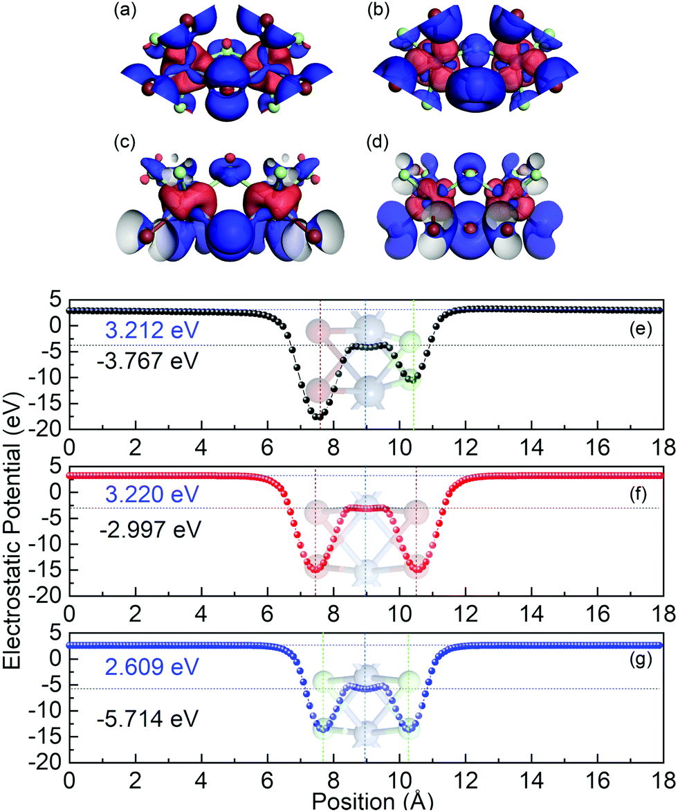 | ||
| Fig. 2 (a–d) Wave functions of ML Cr2Cl3I3 with HSE06 at the VBM (top (a) and side (c) views) and CBM (top (b) and side (d) views) positions. Red and blue colors represent the sign of the wave functions, and the isovalue is 0.006 e Å−3. The xy-averaged electrostatic potential of ML (e) Cr2Cl3I3, (f) CrI3 and (g) CrCl3 calculated by HSE06. The black and blue dashed horizontal lines represent the vacuum energy level and Fermi level, respectively. The coffee, blue and green dashed vertical lines represent the position of the I, Cr and Cl atoms, respectively. | ||
As the Cr atom has d electrons, spin–orbit coupling (SOC) is also taken into consideration. The corresponding band structures are shown in Fig. S5 provided in the ESI.† The indirect band gap of ML Cr2Cl3I3 is reduced to 1.792 eV compared with the original value without SOC of 2.111 eV, because of the orbital splitting at the VBM and CBM with SOC. There is obvious spin–orbit splitting consisting of py, px, and dyz orbitals at the K point, and the corresponding spin–orbit splitting is 0.119 eV. The VBM changes from the original K point to the midpoint along Γ–F symmetry lines, because of the SOC effect. The new VBM consists of pz, dyz, and dxz orbitals. Moreover, there is spin–orbit splitting at the gamma point, which consists of dz2, dyz, and dxz orbitals located at 1.471 eV (splitting of 0.119 eV) and 2.910 eV (splitting of 0.047 eV) above the Fermi-level. For the K point, there is spin–orbit splitting located at 1.082 eV (0.056 eV splitting) and 2.931 eV (0.066 eV splitting), which consists of dz2, dyz, and dxz orbitals. More details can be found in Fig. S5 (ESI†).
In order to evaluate the work function of Cr2Cl3I3, the xy-averaged electrostatic potential is also calculated, as shown in Fig. 2(e). The Fermi-level is −3.767 eV, and the vacuum energy level is 3.212 eV. The work function (W) is defined as: Φ = Evacuum − EF. Evacuum is defined as the vacuum energy level, and EF represents the Fermi-level. The obtained Φ is 6.979 eV, compared to CrCl3 (8.323 eV) and CrI3 (6.217 eV). There are two valleys in the xy-averaged electrostatic potential with different depths, which is different from CrCl3 and CrI3 monolayers where two identical valleys appear. This is caused by the Janus structure of Cr2Cl3I3. One side is I atoms, while the other side is Cl atoms. The first deeper valley is located at 7.600 Å, which corresponds to the location of the I atoms. The other valley is located at the position 9.005 Å, which corresponds to the position of the Cr atoms. Additionally, there are two small peaks located at 8.583 Å and 9.568 Å, respectively, which is consistent with the geometry of ML Cr2Cl3I3. The third shallower valley is located at 10.412 Å, which corresponds to the location of the Cl atoms. Compared with CrCl3 (Fig. 3g) and CrI3 (Fig. 3f), the averaged electrostatic potential (including two smaller local peaks and valleys) shows an unsymmetrical property, as the Janus structure breaks the plane symmetry.
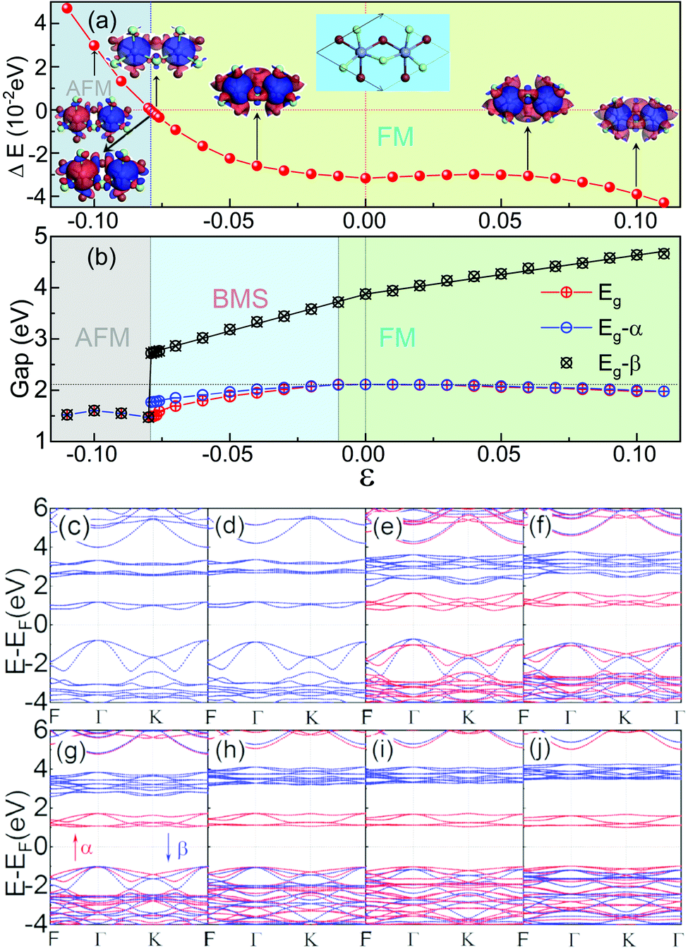 | ||
| Fig. 3 (a) ΔE and (b) the energy gap of ML Cr2Cl3I3 vary with the biaxial strain, ranging from −11% to 11%. The band structure of ML Cr2Cl3I3 under biaxial strains of (c) −10%, (d) −8%, (e) −7.9%, (f) −4%, (g) −2%, (h) 4%, (i) 6% and (j) 10%. The insets of figure (a) present the spin densities of Cr2Cl3I3 under biaxial strains of −10%, −8%, −7.9%, −4%, 6% and 10%, respectively. Here, the isovalue is 0.02 e Å−3. The grey and blue areas represent the AFM and FM ground states of ML Cr2Cl3I3, respectively. The red circles with a cross, the blue circles with a line, and the black circles with a diagonal cross represent the gap, and the gap of spin-α and spin-β electrons, respectively. | ||
3.2. Effect of biaxial strain
Low-dimensional materials are usually synthesized and investigated on all kinds of substrates. Usually, there is a lattice mismatch between the supported 2D material and the underlying substrate, which introduces strain into the 2D material. The strain will further tune the properties of the 2D material by changing the bonding properties.72 Therefore, it is highly desirable to investigate the effects of strain on the properties of 2D materials.72 To address this issue, we first study the effect of biaxial strains (ε) on the magnetic and electronic properties of ML Cr2Cl3I3, as shown in Fig. 3. ε = (a − a0)/a0 is applied on ML Cr2Cl3I3, where a and a0 are the lattice constants with and without strain, respectively. The biaxial compressive strain could transform the ground state of ML Cr2Cl3I3 from the FM to the AFM state. As the biaxial compressive strain increases it enforces the super-exchange interaction. Therefore, the AFM order is enhanced. ML Cr2Cl3I3 could also be transferred from a HSC to a BMS, and even to a spin-unpolarized SC, as the compressive ε monotonically increases. The band gap first increases and then decreases, because of the change of the bond strength.60 For ε = −1%, ML Cr2Cl3I3 is still a direct semiconductor with a gap of 2.112 eV, but the energy level of the CBM (the midpoint along Γ–K symmetry lines, EQ for short) is 0.01 eV lower than the K point (EK). The VBM of the spin-β channel is 0.040 eV higher than that of the spin-α channel, while the VBMs of the spin-α and spin-β channels have the same value, in the absence of the applied strain. As a result, the ML Cr2Cl3I3 has converted from a HSC to a BMS whose CBM and VBM are contributed by different spin channels. For ε = −3% and −2%, the corresponding band gaps are 2.016 and 2.071 eV, with the energy difference between EK and EQ being increased from 0.033 eV to 0.063 eV, respectively. The corresponding energy level splitting is also increased to 0.096 and 0.073 eV at the Γ point, as shown in Fig. 3(g). For ε = −4% and −5%, the band gaps are 1.948 and 1.887 eV, respectively, as shown in Fig. 3(f). The splitting energies are further increased from 0.127 to 0.173 eV. When ε is increased to −6%, the corresponding band gap is further decreased to 1.795 eV, and the energy difference between EK and EQ is increased to 0.150 eV. The corresponding splitting energy is 0.209 eV. For ε = −7%, −7.6%, −7.7%, −7.8%, and −7.9%, the corresponding gap is 1.691, 1.591, 1.514, 1.493 and 1.489 eV, respectively. The corresponding spin splitting energy is 0.253, 0.284, 0.289, 0.300 and 0.366 at the Γ point, respectively. For the biaxial compressive strains in the range of −1% to −7.9%, the corresponding spin splitting energy monotonously increases as the strain increases. When the compressive strain is increased to −8.0% (as shown in Fig. 3(d)), ΔE of ML Cr2Cl3I3 increases from −0.032 eV (0) to −0.030 eV (−2%), −0.026 eV (−4%), −0.009 eV (−7%), −0.004 eV (−7.6%), −0.003 eV (−7.7%), −0.001 eV (−7.8%), −0.0004 eV (−7.9%) and 0.0008 eV (−8.0%), as shown in Fig. 3(a). The corresponding energy difference between the spin-β and α electrons is 1.762, 1.614, 1.502, 1.392, 1.315, 1.220, 1.109, 1.014, 0.975, 0.971, 0.967, 0.955, and 0 eV (−11% < ε < −8%). The corresponding TC is 40.8, 39.4, 38.2, 36.2, 33.4, 28.9, 21.6, 11.9, 4.5, 3.2, 1.9, 0.5 K and 1.1 K (TN), respectively. This means that the FM state is tuned into the AFM ground state as the biaxial compressive strain increases to −8%. Compared with CrI3 (−5.7%)40 and CrCl3 (−2.5%,40 −2.6%71), this value is larger. It originates from the adopted the hybrid functional-HSE06, instead of PBE or PBE+U.71 As the compressive strain continues to increase, the corresponding gap is increased to 1.550 eV (−9%), 1.601 eV (−10%) and 1.520 eV (−11%). The corresponding ΔE is 0.013, 0.030 and 0.047 eV, respectively, and the systems are tuned into the spin-unpolarized state. The corresponding TN is 17.11, 38.4, and 60.6 K, respectively. As the strain increases, the VBM composed of px, py and pz orbitals of I atoms is still located at the Γ point, while the CBM composed of dxz, dyz, dxy, and dx2−y2 orbitals of Cr atoms is transferred from the original K point to the midpoint along Γ–K symmetry lines.Under tensile strain, ΔE first decreases (1%, 4%), and then increases (5%, 11%) as the strain increases, as shown in Fig. 3(a). For ε = 1–4%, the corresponding gap is 2.109, 2.103, 2.100, and 2.079 eV, respectively. At ε = 5%, 6%, 7%, 8%, 9%, 10%, and 11%, the gap is 2.062, 2.048, 2.043, 2.019, 2.000, 1.977 and 1.975 eV, respectively. The gap of spin-α electrons monotonously decreases, while the gap of spin-β electrons monotonously increases. The gap follows a linear relationship: Eg-β = 3.883 + 14.582ε (−8% < ε < 0), Eg-β = 3.895 + 7.408ε (0 < ε < 11%), when ε is in the range of (−11%, 11%). The relationship between Eg-α and ε follows a quadratic function: Eg-α = 2.110 + 0.366ε − 50.319ε2 (−8% < ε < 0). As the strain increases, the VBM composed of px, py and pz orbitals of the I atoms is still located at the Γ point, while the CBM composed of dxz, dyz, dxy, and dx2 orbitals of Cr atoms is transferred from the original K point to the midpoint along the Γ–K symmetry line. The corresponding results are shown in Fig. 3(c)–(g).
ΔE first decreases and then increases as the tensile biaxial strain increases. The corresponding ΔE is −0.031, −0.031, −0.030 and −0.029 eV, respectively, when ε = 1–4%. For ε = 5–11%, the corresponding ΔE is −0.030, −0.031, −0.032, −0.033, −0.036, −0.039, and −0.043 eV, respectively. The critical temperature is closely related to ΔE. As the biaxial strain increases, TC first decreases (0% < ε < 3%) and then increases as the biaxial strain exceeds 3%. For ε = 1–3%, the corresponding TC is 35.5, 35.0, and 34.5 K, respectively. As the biaxial strain further increases, the corresponding TC is 34.2, 34.4, 35.0, 36.3, 38.3, 41.0, and 44.7 K. For a larger ε of 16%, the corresponding TC can go up to 82.6 K. This is caused by the enhancement of the direct exchange interaction between Cr atoms with increasing biaxial tensile strain. The corresponding FM order is also enhanced, so TC tends to increase (Fig. 4).
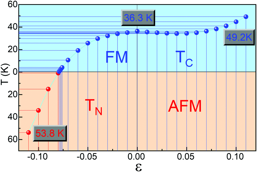 | ||
| Fig. 4 The critical temperature of ML Cr2Cl3I3 as a function of biaxial strain. Different colors show different magnetic ground states. The blue and red areas represent the FM and AFM ground state, respectively. The insets present the corresponding critical temperatures. The red and blue dots represent the corresponding Néel and Curie temperature, respectively. | ||
3.3. Effect of the stacking orders
BL Cr2Cl3I3 is the smallest Cr2Cl3I3 multilayer system stacked by vdW interactions. It is interesting to know: (i) what are the magnetic and electronic properties of BL Cr2Cl3I3 and (ii) are the magnetic and electronic properties of BL Cr2Cl3I3 also closely related to the stacking configurations.Moreover, CrX3 (X = I, Br, Cl) is usually synthesized with multilayers stacked together by vdW interactions.6,9,14,22–28,30,31,35,53,73,74 So the stacking-induced modifications of the properties need to be systemically discussed. Taking BL MoSSe as a reference,11 six different stacking patterns (AA-II, AA-ClI, AA-ClCl, AB-ClI, AB-II and AB-ClCl) of BL Cr2Cl3I3 are considered, and the optimized geometries are shown in Fig. 5a–f, respectively. The interlayer vertical distance of the plane of the I (Cl) and Cl (I) atoms d is defined to describe the interaction between the Cr2Cl3I3 layers. The corresponding distance and binding energies calculated by the DFT-D2,58 DFT-D3,30–32 and DFT-TS33 methods are shown in Table 1. We can find that the AB-ClCl configuration has the smallest d = 3.01 Å calculated by DFT-D2, which is smaller than AA-II (3.145 Å) and AA-ClI (3.123 Å), AA-ClCl (3.743 Å), AB-ClI (3.807 Å), and AB-II (3.806 Å). Eb is defined as Eb = EBL − EML × 2, where EBL is the total energy of the relaxed bilayer Cr2Cl3I3. The corresponding Eb for the AB-II configuration is −0.990 eV, while the corresponding values of AA-II, AA-ClI, AA-ClCl, AB-ClI, and AB-ClCl are −0.938, −0.755, −0.629, −0.810, and −0.676 eV, respectively. Therefore, the AB-II configuration is the most stable one, which is different from CrI332 and CrCl3.75 This may be caused by the symmetry breaking of Janus Cr2Cl3I3. Other optimized vdW functionals (such as DFT-D330–32) and self-consistent screening of the Tkatchenko–Scheffler method (TS33) are also adopted to investigate BL Cr2Cl3I3, and they show the same trend. The Eb calculated by DFT-D3 for the AB-II configuration with distance 3.603 Å is −0.549 eV, while the corresponding Eb of AA-II, AA-ClI, AA-ClCl, AB-ClI and AB-ClCl is −0.487, −0.439, −0.340, −0.465 and −0.415 eV, respectively. A similar trend also appears in the DFT-TS results. The AB-II configuration is still the most stable one among the six geometries. All the results are collected in Table 1. Therefore, the discussion is established based on the DFT-D2 results in the following part. The magnetic and electronic properties are usually related to the stacking orders of 2D materials. We also investigate the magnetic order of BL Cr2Cl3I3, and the corresponding spin densities are shown in the middle set of Fig. 5. The stable magnetic orders are related to the stacking orders. AA-ClI, AA-ClCl, AB-ClI, AB-II and AB-ClCl show a FM ground state, which is defined as one Cr2Cl3I3 layer ferromagnetically coupled with another. The total magnetic moment is 12.00 μB, and each layer of Cr2Cl3I3 contributes 6.00 μB. The magnetic moment mainly localizes at the Cr atoms, as shown in the spin densities of BL Cr2Cl3I3 in Fig. 5. The corresponding ΔE is positive. AA-II shows AFM ground order, which implies one layer antiferromagnetically couples with another. The corresponding ΔE is −0.003 eV, and the total magnetic moment is 0 μB, as one layer contributes 6.00 μB and another layer contributes −6.00 μB. No matter what the magnetic order is, all BL Janus Cr2Cl3I3 are BMSs. There are three important parameters: Δ1, Δ2 and Δ3, to characterize BMSs, as shown in Fig. S6 (ESI†), which are defined in the early work.8,62,63 For AB-II, the corresponding Δ1, Δ2 and Δ3 are 2.111, 0.038 and 1.795 eV, respectively. AA-II is a BMS with an AFM ground state. Most BMSs have a FM ground state,76 while an AFM BMS is quite rare. The corresponding Δ1, Δ2 and Δ3 are 0.075, 0.254 and 1.229 eV, respectively. Δ1 is quite small, so it's easy to tune the BMS into a half-metal. It should be noted here that Δ3 is big enough to ensure the stability of the half-metallicity. For all the stacking orders, the gaps of the spin-α and spin-β channels are larger than the global band gap (Table 2).
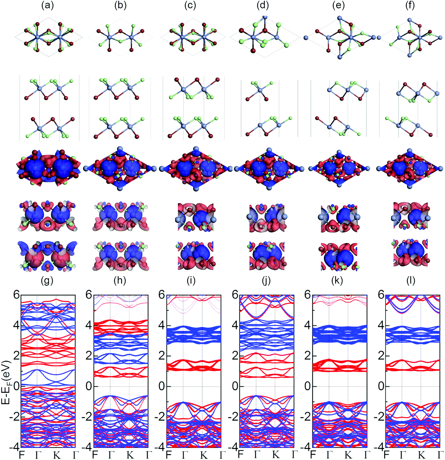 | ||
| Fig. 5 (a–f) The optimized geometries of BL Cr2Cl3I3 with different stacking orders with top and side views. The stacking orders of (a) AA-II, (b) AA-ClI, (c) AA-ClCl, (d) AB-ClI, (e) AB-II, and (f) AB-ClCl are shown in top and side views. (g–l) The spin densities with the FM ground state of the corresponding structures are shown in (g) AA-II, (h) AA-ClI, (i) AA-ClCl, (j) AB-ClI, (k) AB-II, and (l) AB-ClCl. The bottom set is the corresponding band structures. The isovalue is 0.02 e Å−3. The red and blue lines represent the contribution of spin-α and spin-β electrons, respectively. | ||
| System | DFT-D2 | DFT-D3 | TS | |||
|---|---|---|---|---|---|---|
| d 0 (Å) | E b (eV) | d 0 (Å) | E b (eV) | d 0 (Å) | E b (eV) | |
| AA-II | 3.145 | −0.938 | 3.111 | −0.487 | 3.681 | −0.503 |
| AA-ClI | 3.123 | −0.755 | 3.073 | −0.439 | 3.395 | −0.456 |
| AA-ClCl | 3.743 | −0.629 | 3.807 | −0.340 | 3.362 | −0.354 |
| AB-ClI | 3.807 | −0.810 | 3.708 | −0.465 | 3.32 | −0.491 |
| AB-II | 3.806 | −0.990 | 3.603 | −0.549 | 3.698 | −0.520 |
| AB-ClCl | 3.010 | −0.676 | 2.977 | −0.415 | 3.079 | −0.397 |
| System | Magnetic | ΔE (meV) | Gap (eV) | Gap-α (eV) | Gap-β (eV) |
|---|---|---|---|---|---|
| AA-II | AFM | −3.0 | 0.075 | 1.350 | 0.325 |
| AA-ClI | FM | 2.0 | 1.221 | 1.233 | 2.107 |
| AA-ClCl | FM | 1.0 | 2.071 | 2.080 | 3.813 |
| AB-ClI | FM | 70.0 | 1.180 | 1.190 | 2.910 |
| AB-II | FM | 8.0 | 1.991 | 2.013 | 3.786 |
| AB-ClCl | FM | 2.0 | 2.049 | 2.065 | 3.792 |
3.4. Stability of Janus Cr2Cl3I3
The dynamical stability of ML Cr2Cl3I3 is confirmed via computing the phonon dispersion curves and phonon density of states, which show no imaginary phonon modes (Fig. 6a). The highest vibration frequency is 9.09 THz, which is higher than ML CrI3 (7.32 THz), but smaller than CrCl3 (10.95 THz), as shown in Fig. S7 (ESI†), reflecting the mechanical robustness of the covalent bonds. Meanwhile, certain phonon modes of Cr2Cl3I3 are absent because of the breaking of mirror symmetry, which reduces the lattice from point group D3d to C3v, compared with CrI3 and CrCl3, as shown in Fig. S7 (ESI†).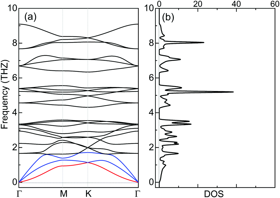 | ||
| Fig. 6 (a) Phonon spectrum, and (b) phonon density of states (PHDOS) of ML Cr2Cl3I3. | ||
The thermal stability of Cr2Cl3I3 is also examined via ab initio molecular dynamics (AIMD) simulations. The simulated temperatures are 300, 500 and 700 K. The fluctuations of the total energy of Cr2Cl3I3 at 300, 500 and 700 K are shown in Fig. 7(a)–(c), respectively. During the simulation progress, the sandwich-like structure of ML Janus Cr2Cl3I3 remains intact at room temperature, and the total energy oscillates around −34.41 eV. The maximum energy fluctuation is 0.38 eV. The energy oscillates around −34.13 eV and the energy fluctuation is 0.65 eV at 500 K. The snapshots of ML Cr2Cl3I3 are also presented, showing intact structures. In a word, the structures are well kept without obvious distortions in the simulated time (10 ps) at 300 K, 500 K and 700 K, as shown in Fig. 7. We note that the use of a periodic boundary condition in AIMD simulations with a relatively small system size can artificially increase the stability of the structures. A larger supercell (2 × 2 × 1 cell) is also adopted, and it shows similar results to the unit cell.
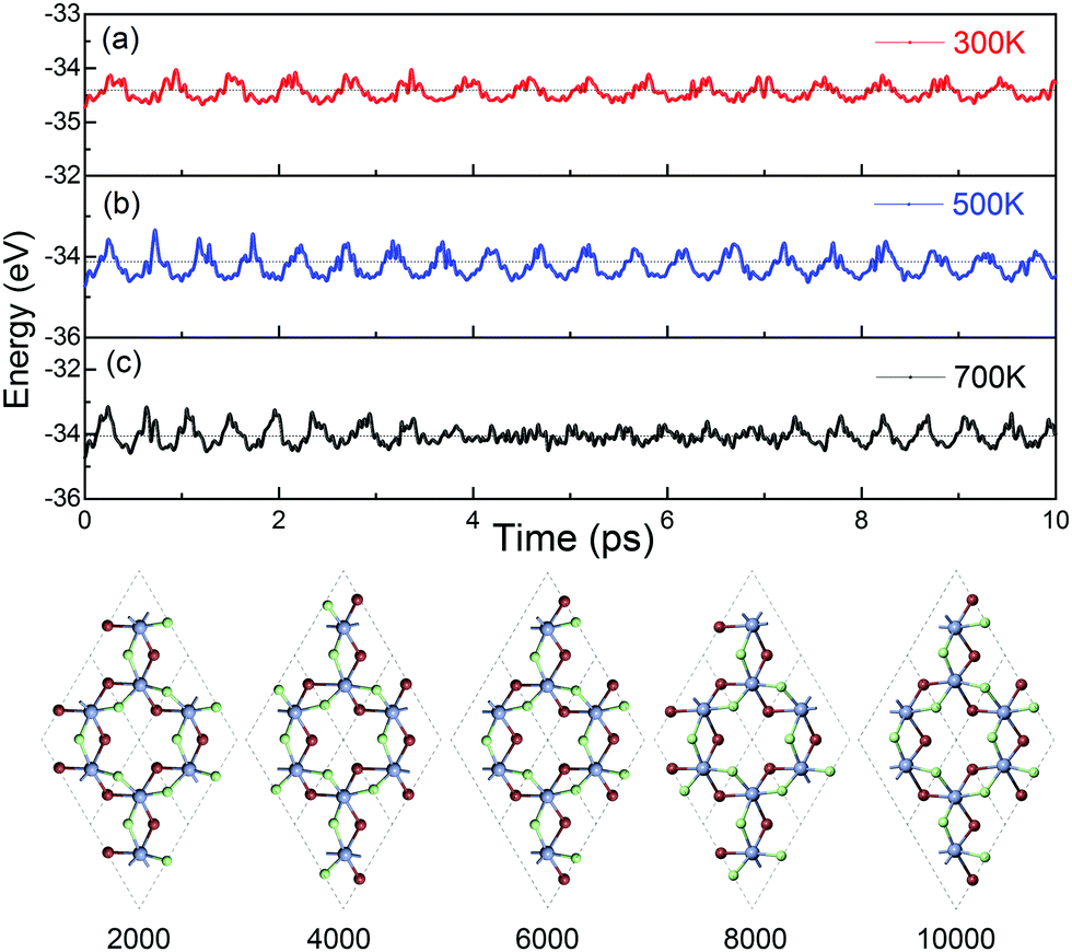 | ||
| Fig. 7 Ab initio MD simulations of the evolution of the energy of ML Cr2Cl3I3 under temperatures of (a) 300 K, (b) 500 K, and (c) 700 K. The total time is 10 ps. The bottom is the top views of simulation snapshots at 2, 4, 6, 8 and 10 ps of ab initio MD simulations at 300 K. | ||
3.5. Synthetization of Janus Cr2Cl3I3
2D Janus TMDs, such as MoSSe is synthesized by selenizing the MoS2 monolayer77 or substituted MoSe2 monolayer with sulfurization.78 Janus Cr2Cl3I3 monolayers should be also synthesized by replacing the top-layer I atoms with Cl atoms through chlorinating the CrI3 monolayer in chemical vapor deposition.4. Conclusions
In conclusion, we examine the geometric, magnetic, and electronic properties of Janus Cr2Cl3I3 with first-principles calculations. ML Cr2Cl3I3 is a HSC with a direct band gap of 2.111 eV, showing an obvious electron spin-polarization. The electronic properties of ML Cr2Cl3I3 could be effectively modulated by biaxial strains, from the HSC into a BMS, and even to a spin-unpolarized SC. As the compressive biaxial strain increases, ML Cr2Cl3I3 is tuned from the FM to the AFM ground state (ε ≥ 7.9%). The corresponding TC is 36.3 K. As the biaxial compressive and tensile strains are increased to 10%, the corresponding critical temperatures are 53.8 (TN) and 49.2 K (TC), respectively. Moreover, the magnetic configuration and electronic properties could also be effectively modulated by the stacking orders. For BL Cr2Cl3I3, the most stable AB-II configuration presents a FM ground state. BL Cr2Cl3I3 in all considered stacking orders is a BMS. Last, the phonon spectrum and AIMD confirm the dynamical and thermal stability of Cr2Cl3I3. The modulated magnetic and electronic properties imply that Janus Cr2Cl3I3 should be a promising candidate material for 2D spintronic devices.Conflicts of interest
The authors declare no competing financial interest.Acknowledgements
We thank Doctor Yang Li, Prof. Xingxing Li, and Chen Si for helpful discussion. This work was partially supported by the financial support from the Natural Science Foundation of China (Grant No. 11904203), the Fundamental Research Funds of Shandong University (Grant No. 2019GN065), the President foundation of China Academy of Engineering Physics (YZJJLX2016004), China Postdoctoral Science Foundation (No. 2019M650619) and the National Key Research and Development Program of China (Grant No. 2016YFB0201203). The Shanghai Supercomputer Center, National Supercomputing Centers of Guangzhou, and Supercomputer Centers of Tsinghua and Shandong University should be acknowledged.References
- V. Gusynin and S. Sharapov, Phys. Rev. Lett., 2005, 95, 146801 CrossRef CAS PubMed
.
- T. Mukherjee, S. Chowdhury, D. Jana and L. C. L. Y. Voon, J. Phys.: Condens. Matter, 2019, 31, 335802 CrossRef CAS PubMed
- S. C. Zhang, T. H. Hansson and S. Kivelson, Phys. Rev. Lett., 1989, 62, 82 CrossRef CAS PubMed
- A. K. Geim, Science, 2009, 324, 1530–1534 CrossRef CAS PubMed
- A. C. Neto, F. Guinea, N. M. Peres, K. S. Novoselov and A. K. Geim, Rev. Mod. Phys., 2009, 81, 109 CrossRef
- L. Ci, L. Song, C. Jin, D. Jariwala, D. Wu, Y. Li, A. Srivastava, Z. F. Wang, K. Storr, L. Balicas, F. Liu and P. M. Ajayan, Nat. Mater., 2010, 9, 430–435 CrossRef CAS PubMed
- Z. Guan, J. Wang, J. Huang, X. Wu, Q. Li and J. Yang, J. Phys. Chem. C, 2014, 118, 22491–22498 CrossRef CAS
- Z. Guan, W. Wang, J. Huang, X. Wu, Q. Li and J. Yang, J. Phys. Chem. C, 2014, 118, 28616–28624 CrossRef CAS
- M. Liao, Y. Zang, Z. Guan, H. Li, Y. Gong, K. Zhu, X.-P. Hu, D. Zhang, Y. Xu, Y.-Y. Wang, K. He, X.-C. Ma, S.-C. Zhang and Q.-K. Xue, Nat. Phys., 2018, 14, 344–348 Search PubMed
- N. Luo, W. Duan, B. I. Yakobson and X. Zou, Adv. Funct. Mater., 2020, 2000533–2000541, DOI:10.1002/adfm.202000533
- Z. Guan, S. Ni and S. Hu, J. Phys. Chem. C, 2018, 122, 6209–6216 CrossRef CAS
- D. Golberg, Y. Bando, Y. Huang, T. Terao, M. Mitome, C. Tang and C. Zhi, ACS Nano, 2010, 4, 2979–2993 CrossRef CAS PubMed
- N. D. Mermin and H. Wagner, Phys. Rev. Lett., 1966, 17, 1133–1136 CrossRef CAS
- C. Gong, L. Li, Z. Li, H. Ji, A. Stern, Y. Xia, T. Cao, W. Bao, C. Wang, Y. Wang, Z. Q. Qiu, R. J. Cava, S. G. Louie, J. Xia and X. Zhang, Nature, 2017, 546, 265 CrossRef CAS PubMed
- Y. Hou, J. Kim and R. Wu, Sci. Adv., 2019, 5, eaaw1874 CrossRef PubMed
- M. Ge, Y. Su, H. Wang, G. Yang and J. Zhang, RSC Adv., 2019, 9, 14766–14771 RSC
- Z. Zhang, X. Ni, H. Huang, L. Hu and F. Liu, Phys. Rev. B: Condens. Matter Mater. Phys., 2019, 99, 115441 CrossRef CAS
- H. Zhang, W. Qin, M. Chen, P. Cui, Z. Zhang and X. Xu, Phys. Rev. B: Condens. Matter Mater. Phys., 2019, 99, 116003 Search PubMed
- P. Jiang, C. Wang, D. Chen, Z. Zhong, Z. Yuan, Z.-Y. Lu and W. Ji, Phys. Rev. B: Condens. Matter Mater. Phys., 2019, 99, 144401–144409 CrossRef CAS
- S. Chen, C. Huang, H. Sun, J. Ding, P. Jena and E. Kan, J. Phys. Chem. C, 2019, 123, 17987–17993 CrossRef CAS
- Z. Sun, Y. Yi, T. Song, G. Clark, B. Huang, Y. Shan, S. Wu, D. Huang, C. Gao, Z. Chen, M. McGuire, T. Cao, D. Xiao, W.-T. Liu, W. Yao, X. Xu and S. Wu, Nature, 2019, 572, 497–501, DOI:10.1038/s41586-019-1445-3
- D. Ghazaryan, M. T. Greenaway, Z. Wang, V. H. Guarochico-Moreira, I. J. Vera-Marun, J. Yin, Y. Liao, S. V. Morozov, O. Kristanovski, A. I. Lichtenstein, M. I. Katsnelson, F. Withers, A. Mishchenko, L. Eaves, A. K. Geim, K. S. Novoselov and A. Misra, Nat. Electron., 2018, 1, 344–349 CrossRef CAS
- S. Jiang, J. Shan and K. F. Mak, Nat. Mater., 2018, 17, 406–411 CrossRef CAS PubMed
- M. Bonilla, S. Kolekar, Y. Ma, H. C. Diaz, V. Kalappattil, R. Das, T. Eggers, H. R. Gutierrez, P. Manh-Huong and M. Batzill, Nat. Nanotechnol., 2018, 13, 289–294 CrossRef CAS PubMed
- B. Huang, G. Clark, E. Navarro-Moratalla, D. R. Klein, R. Cheng, K. L. Seyler, D. Zhong, E. Schmidgall, M. A. McGuire, D. H. Cobden, W. Yao, D. Xiao, P. Jarillo-Herrero and X. Xu, Nature, 2017, 546, 270–285 CrossRef CAS PubMed
- S. Jiang, L. Li, Z. Wang, J. Shan and K. F. Mak, Nat. Electron., 2019, 2, 159–163 CrossRef
- K. S. Burch, Nat. Nanotechnol., 2018, 13, 532 CrossRef CAS PubMed
- B. Huang, G. Clark, D. R. Klein, D. MacNeill, E. Navarro-Moratalla, K. L. Seyler, N. Wilson, M. A. McGuire, D. H. Cobden, D. Xiao, W. Yao, P. Jarillo-Herrero and X. Xu, Nat. Nanotechnol., 2018, 13, 544–549 CrossRef CAS PubMed
- Z. Wang, I. Gutierrez-Lezama, N. Ubrig, M. Kroner, M. Gibertini, T. Taniguchi, K. Watanabe, A. Imamoglu, E. Giannini and A. F. Morpurgo, Nat. Commun., 2018, 9, 2516–2523 CrossRef PubMed
- J.-H. Yang and H. Xiang, Nat. Mater., 2019, 12, 1273–1274, DOI:10.1038/s41563-019-0524-z
- B. Huang, J. Cenker, X. Zhang, E. L. Ray, T. Song, T. Taniguchi, K. Watanabe, M. A. McGuire, D. Xiao and X. Xu, Nat. Nanotechnol., 2020, 3, 212–216, DOI:10.1038/s41565-019-0598-4
- N. Sivadas, S. Okamoto, X. Xu, C. J. Fennie and D. Xiao, Nano Lett., 2018, 18, 7658–7664 CrossRef CAS PubMed
- Z. Guan, S. Ni and S. Hu, RSC Adv., 2017, 7, 45393–45399 RSC
- J. He, G. Ding, C. Zhong, S. Li, D. Li and G. Zhang, J. Mater. Chem. C, 2019, 7, 5084–5093 RSC
- M. Gibertini, M. Koperski, A. F. Morpurgo and K. S. Novoselov, Nat. Nanotechnol., 2019, 14, 408–419 CrossRef CAS PubMed
- F. Zheng, J. Zhao, Z. Liu, M. Li, M. Zhou, S. Zhang and P. Zhang, Nanoscale, 2018, 10, 14298–14303 RSC
- D. Soriano, C. Cardoso and J. Fernández-Rossier, Solid State Commun., 2019, 299, 113662 CrossRef CAS
- I. Lee, F. G. Utermohlen, D. Weber, K. Hwang, C. Zhang, J. van Tol, J. E. Goldberger, N. Trivedi and P. C. Hammel, Phys. Rev. Lett., 2020, 124, 017201 CrossRef CAS PubMed
- J. L. Lado and J. Fernández-Rossier, 2D Mater., 2017, 4, 035002 CrossRef
- L. Webster and J.-A. Yan, Phys. Rev. B: Condens. Matter Mater. Phys., 2018, 98, 144411 CrossRef CAS
- L. Dong, J. Lou and V. B. Shenoy, ACS Nano, 2017, 11, 8242–8248 CrossRef CAS PubMed
- Y. Guo, S. Zhou, Y. Bai and J. Zhao, Appl. Phys. Lett., 2017, 110, 163102 CrossRef
- Y. C. Cheng, Z. Y. Zhu, M. Tahir and U. Schwingenschlögl, EPL, 2013, 102, 57001 CrossRef
- W. Chen, X. Hou, X. Shi and H. Pan, ACS Appl. Mater. Interfaces, 2018, 10, 35289–35295 CrossRef CAS PubMed
- K. Ren, S. Wang, Y. Luo, J.-P. Chou, J. Yu, W. Tang and M. Sun, J. Phys. D: Appl. Phys., 2020, 53, 185504 CrossRef CAS
- R. Li, Y. Cheng and W. Huang, Small, 2018, 14, 1802091 CrossRef PubMed
- Y. Liu, Y. Huang and X. Duan, Nature, 2019, 567, 323–333 CrossRef CAS PubMed
- M. Idrees, H. U. Din, R. Ali, G. Rehman, T. Hussain, C. V. Nguyen, I. Ahmad and B. Amin, Phys. Chem. Chem. Phys., 2019, 21, 18612–18621 RSC
- W. Guo, X. Ge, S. Sun, Y. Xie and X. Ye, Phys. Chem. Chem. Phys., 2020, 22, 4946–4956 RSC
- Z. Guan, C.-S. Lian, S. Hu, S. Ni, J. Li and W. Duan, J. Phys. Chem. C, 2017, 121, 3654–3660 CrossRef CAS
- Z. Guan and S. Ni, Appl. Phys. A: Mater. Sci. Process., 2017, 123, 678 CrossRef
- Z. Lin, C. Si, S. Duan, C. Wang and W. Duan, Phys. Rev. B: Condens. Matter Mater. Phys., 2019, 100, 155408 CrossRef CAS
- T. Song, X. Cai, M. W.-Y. Tu, X. Zhang, B. Huang, N. P. Wilson, K. L. Seyler, L. Zhu, T. Taniguchi, K. Watanabe, M. A. McGuire, D. H. Cobden, D. Xiao, W. Yao and X. Xu, Science, 2018, 360, 1214–1218 CrossRef CAS PubMed
- M. Wu, Z. Li, T. Cao and S. G. Louie, Nat. Commun., 2019, 10, 10325–10327 Search PubMed
- S. Baidya, J. Yu and C. H. Kim, Phys.
Rev. B: Condens. Matter Mater. Phys., 2018, 98, 155148 CrossRef CAS
- L. Chen, J.-H. Chung, B. Gao, T. Chen, M. B. Stone, A. I. Kolesnikov, Q. Huang and P. Dai, Phys. Rev. X, 2018, 8, 041028 CAS
- Y. Baskin and L. Meyer, Phys. Rev., 1955, 100, 544 CrossRef CAS
- S. Grimme, J. Comput. Chem., 2006, 27, 1787–1799 CrossRef CAS PubMed
- R. Zacharia, H. Ulbricht and T. Hertel, Phys. Rev. B: Condens. Matter Mater. Phys., 2004, 69, 155406 CrossRef
- J. Heyd, G. E. Scuseria and M. Ernzerhof, J. Chem. Phys., 2003, 118, 8207–8215 CrossRef CAS
- J. Heyd, G. E. Scuseria and M. Ernzerhof, J. Chem. Phys., 2006, 124, 219906 CrossRef
- Z. Guan, S. Ni and S. Hu, ACS Omega, 2019, 4, 10293–10301 CrossRef CAS PubMed
- Z. Guan, C. Si, S. Hu and W. Duan, Phys. Chem. Chem. Phys., 2016, 18, 12350–12356 RSC
- Z. Guan, S. Ni and S. Hu, ACS Omega, 2020, 5, 5900–5910 CrossRef CAS PubMed
- G. Kresse and J. Furthmüller, Phys. Rev. B: Condens. Matter Mater. Phys., 1996, 54, 11169–11186 CrossRef CAS PubMed
- G. Kresse and J. Furthmüller, Comput. Mater. Sci., 1996, 6, 15–50 CrossRef CAS
- J. P. Perdew, K. Burke and M. Ernzerhof, Phys. Rev. Lett., 1996, 77, 3865–3868 CrossRef CAS PubMed
- H. J. Monkhorst and J. D. Pack, Phys. Rev. B: Condens. Matter Mater. Phys., 1976, 13, 5188–5192 CrossRef
- A. Togo and I. Tanaka, Scr. Mater., 2015, 108, 1–5 CrossRef CAS
- S. Nosé, J. Chem. Phys., 1984, 81, 511–519 CrossRef
- Z. Wu, J. Yu and S. Yuan, Phys. Chem. Chem. Phys., 2019, 21, 7750–7755 RSC
- C. Si, Z. Sun and F. Liu, Nanoscale, 2016, 8, 3207–3217 RSC
- C. Bao and S. Zhou, Nat. Mater., 2020, 19, 263–264, DOI:10.1038/s41563-020-0614-y
- L. Thiel, Z. Wang, M. A. Tschudin, D. Rohner, I. Gutierrez-Lezama, N. Ubrig, M. Gibertini, E. Giannini, A. F. Morpurgo and P. Maletinsky, Science, 2019, 364, 973–976 CrossRef CAS PubMed
- H. Wang, V. Eyert and U. Schwingenschloegl, J. Phys.: Condens. Matter, 2011, 23, 116003 CrossRef CAS PubMed
- X. Li, X. Wu, Z. Li, J. Yang and J. G. Hou, Nanoscale, 2012, 4, 5680–5685 RSC
- A.-Y. Lu, H. Zhu, J. Xiao, C.-P. Chuu, Y. Han, M.-H. Chiu, C.-C. Cheng, C.-W. Yang, K.-H. Wei, Y. Yang, Y. Wang, D. Sokaras, D. Nordlund, P. Yang, D. A. Muller, M.-Y. Chou, X. Zhang and L.-J. Li, Nat. Nanotechnol., 2017, 12, 744–749 CrossRef CAS PubMed
- J. Zhang, S. Jia, I. Kholmanov, L. Dong, D. Er, W. Chen, H. Guo, Z. Jin, V. B. Shenoy, L. Shi and J. Lou, ACS Nano, 2017, 11, 8192–8198 CrossRef CAS PubMed
Footnote |
| † Electronic supplementary information (ESI) available: Information on materials, energy with lattice parameters, partial orbital projected band structure, band structure of CrCl3 and CrI3, PDOS, band structure with SOC, band structure under certain strains of the ML Janus Cr2Cl3I3 calculated by the HSE06 functional, phonon spectrum and density of states (calculated by PBE) of CrCl3 and CrI3. See DOI: 10.1039/d0ma00085j |
| This journal is © The Royal Society of Chemistry 2020 |