
 Open Access Article
 This Open Access Article is licensed under a Creative Commons Attribution-Non Commercial 3.0 Unported Licence
Conversion of h-BN into c-BN for tuning optoelectronic properties
Ariful
Haque
 * and
Jagdish
Narayan
* and
Jagdish
Narayan
Materials Science and Engineering, North Carolina State University, Raleigh, North Carolina 27695.7916, USA. E-mail: ahaque@ncsu.edu
First published on 8th May 2020
Abstract
Boron nitride (BN) films containing different percentages of cubic phase contents were grown on a (0001) sapphire substrate using a novel pulsed laser processing method. To synthesize cubic boron nitride (c-BN), the hexagonal boron nitride (h-BN) target was ablated by a pulsed KrF laser (λ = 248 nm) during the pulsed laser deposition process followed by the pulsed laser annealing (PLA) with an ArF laser (λ = 193 nm). We performed a set of detailed characterization analyses on the fabricated BN films by Raman spectroscopy, X-ray diffraction (XRD), high resolution SEM, EBSD, and UV-Vis measurements. Raman spectroscopy was successfully utilized to identify the crystalline quality and to determine the fraction of c-BN phase quantitatively in the BN films. Here, we report that c-BN phase content can be tuned by the laser energy density during the PLA treatment. The optical bandgap of the fabricated BN films was found to increase with increasing cubic phase content and a correlation was obtained between the optical bandgap and the c-BN phase content in the films. The details of the structure–property correlation and the possible applications of these films are discussed.
Introduction
Boron nitride (BN) is a refractory material, which exists in different polymorphic forms and exhibits interesting optical and electronic properties. The phase diagram of BN contains a liquid-h-BN–c-BN triple point at 3500 K and 9.5 GPa pressure, where h-BN can be converted into c-BN.1 Thermodynamic calculations have shown some variance to the triple point, but these calculations involved too many adjustable parameters to draw definite conclusions.2 The sp2 bonded hexagonal and rhombohedral structures as well as the sp3 bonded cubic and wurtzitic structures all exist at different temperatures and pressures in the phase diagram of BN.3 Among these phases the hexagonal boron nitride (h-BN) is structurally analogous to graphite and the cubic boron nitride (c-BN) is isostructural and isoelectronic to diamond. Despite their structural similarities with carbon polymorphs, all the phases of BN are wide bandgap semiconductors with bandgap over 5.0 eV unlike zero bandgap of graphite and related materials. Due to its hardness and chemical inertness (higher resistance to oxidation) to ferrous materials in harsh environments, c-BN is the most desirable one for technological applications.4 The ease of p- and n-type doping and excellent thermal properties also make c-BN an exciting material to be used in high frequency and high power devices, which could be operated under extreme conditions such as high temperature, radiative environments in space or in high chemical erosion environments. The c-BN also has many other possible applications as a heat-conducting substrate, a cold cathode emitter with negative electron affinity, and a component in various UV detectors. However, the bulk cubic phase exists in the high-temperature and high-pressure region of the BN phase diagram (3500 K/9.5 GPa), which is not amenable to thin film applications. The fabrication of high quality single crystal c-BN films has many challenges. Researchers have tried chemical/physical vapor-deposition methods to grow the cubic phase of boron nitride with limited success. With PVD methods, low crystallinity and higher defect densities were observed and the existence of interfacial soft and humidity sensitive h-BN, disordered turbostratic boron nitride (t-BN) and amorphous boron nitride (a-BN) leads to low phase purity in c-BN.5 Unlike for diamond fabrication, the chemical vapor deposition (CVD) techniques of c-BN fabrication have also shown limited success. Only 0.24 μm thick films with around 80% cubic phase content were achieved via the CVD route.6,7 Some success in growing highly crystalline and phase-pure c-BN was reported by ion beam assisted deposition on CVD diamond films but the measured thickness was only about 30 nm.8 To address the aforementioned issues related to structure and quality, we have recently discovered a novel route to fabricate phase-pure c-BN from PLD grown h-BN on a sapphire substrate.9,10 This fabrication technique is based upon the nanosecond laser melting, which occurs during pulsed laser annealing (PLA). In this technique, we use a 193 nm pulsed laser at room temperature and ambient pressure to convert nanocrystalline h-BN into c-BN. In this paper, we have carried out a systematic study to understand the c-BN conversion from nanocrystalline h-BN using different laser energy densities. Depending upon the amount of undercooling we are able to convert h-BN into phase mixtures of h-BN and c-BN with different relative ratios, eventually leading to epitaxial phase-pure c-BN. Since the tuning of the relative ratio and the epitaxial nature of c-BN play a role in the determination of properties, we have carried out detailed characterization and property analysis of the mixed phase and phase-pure c-BN. We have investigated the structure and phase purity of the BN samples using detailed Raman spectroscopy and explored the optical properties using UV-Vis spectroscopy. Because of the dependence of the sensitivity of the Raman signal on the crystalline quality, only thick films with a substantial amount of cubic phase content can be characterized by Raman spectroscopy.11,12 Owing to the improved quality of the BN samples, we have successfully quantified the c-BN phase content for the first time in the BN samples using Raman spectroscopy. Finally, a correlation between the optical bandgap and the fraction of cubic phase in the BN films was established for tuning and bandgap engineering of composite materials for interesting solid state devices.Experimental details
PLD and PLA
Hexagonal boron nitride (h-BN) was deposited on both c and r-sapphire at room temperature using a KrF laser (wavelength = 248 nm, pulse duration = 25 ns) at an energy density of 2.5–3.0 J cm−2 under a base vacuum of 5 × 10⁻⁷ Torr. A high quality dense h-BN target was used to grow the h-BN films with thickness ∼500 nm on the sapphire substrates. These films were irradiated using a pulsed ArF laser (wavelength = 193 nm, pulse duration = 20 ns) in air at energy densities between 0.52 and 0.7 J cm−2 to convert into c-BN nanostructures, microstructures, and large-area thin films. During the laser annealing process, the as-deposited films were melted in a super-undercooled state and subsequently quenched within 200–250 nanoseconds.40,41 The single crystal, sapphire template helped to grow epitaxial single crystal c-BN structures via domain matching epitaxy.Raman spectroscopy
The as-deposited and laser-annealed partially and fully converted c-BN samples were characterized using a WITec confocal Raman microscope system (alpha300M) with a maximum sensitivity excitation wavelength of 532.16 nm to identify the Raman active vibration modes. A crystalline Si sample (with a characteristic Raman peak at 520.6 cm−1) was used to calibrate the Raman spectra.XRD
X-ray diffraction (XRD) was performed using θ/2θ geometry on the phase-pure c-BN thin film using a Rigaku SmartLab X-ray diffractometer with a CuKα X-ray source (25 kV, 15 mA). Diffraction data were collected with a 0.02 step size in the 2θ range of 22°–80° and a constant dwell time of 0.5 second per scan point. Bragg–Brentano reflection geometry was used during the data acquisition process.SEM and EBSD
High-resolution scanning-electron-microscopy (HRSEM) with sub-nanometer resolution was carried out on the laser irradiated samples using the FEI Verios 460L SEM. We also conducted electron backscatter diffraction (EBSD) measurements using a FEI Quanta 3D FEG FIB-SEM system to map out the Kikuchi diffraction patterns for determining the relative film orientations with the substrate and to identify the crystal structures. In this system, an EBSD HKL Nordlys detector with lateral resolution less than 10 nm was used to obtain the Kicuchi diffraction patterns. A stationary electron beam with 15 kV energy and 11 nA current interacted with the tilted sample (70°) and the diffracted electrons from the crystalline surface formed a three-dimensional pattern. The diffraction pattern is characteristic of the crystal structure, and hence this pattern has been used to determine crystal structures and orientation.13Results and discussion
In our study, sample A is the as-deposited phase-pure h-BN, samples B, C and D consist of a phase mixture of c-BN and h-BN annealed at 0.52 J cm−2, 0.56 J cm−2, and 0.60 J cm−2, respectively, and sample E is the phase-pure c-BN which has been annealed at 0.7 J cm−2. A direct conversion of h-BN into phase mixtures of h-BN and c-BN and phase-pure c-BN has been accomplished by 193 nm nanosecond pulsed laser melting at room temperature and atmospheric pressure in air. This first-order phase transformation occurs as a result of quenching from the super undercooled liquid state. According to the equilibrium P vs. T phase diagram, phase transformation from h-BN to c-BN can only be attained in a high-temperature and high-pressure region, as the h-BN, c-BN, and liquid triple point lies at 3500 K/9.5 GPa.14 Thermodynamic calculations by Solozhenko show this triple point at 3700 K/7 GPa; however, a large number of fitting parameters in the calculation raise doubts about the accuracy of these calculations.2The non-equilibrium laser melting of h-BN creates a super-undercooled state and shifts the triple point to as low as 2800 K at atmospheric pressure, which has been calculated using Simulation of Laser Interaction with Materials (SLIM) software developed by Singh and Narayan.15 This super-undercooled state rapidly quenches and leads to the formation of crystalline c-BN. Depending upon the amount of laser energy density used in the PLA process, which determines the amount of undercooling, we can control the volume fraction of h-BN and c-BN in the mixed phase. Finally if we allow enough nucleation and growth time, the liquid phase can completely be converted into phase-pure c-BN.10Fig. 1 shows the SEM micrograph of the fully transformed large area c-BN film.
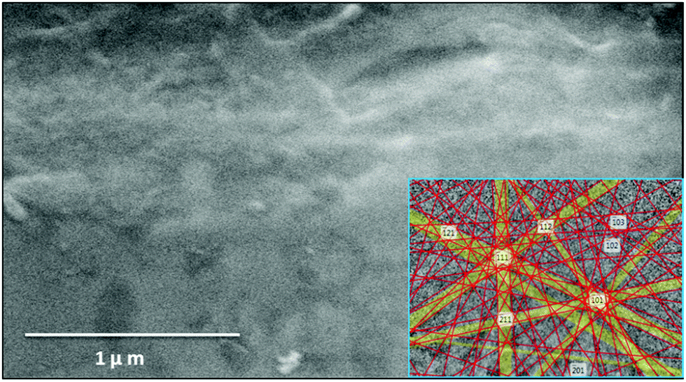 | ||
| Fig. 1 High resolution SEM micrographs of the large area thin film of phase-pure c-BN annealed at 0.7 J cm−2. The inset in figure is showing the EBSD pattern from the phase-pure c-BN confirming the same orientation relationship. | ||
Fig. 2(a) shows the XRD pattern containing (0002) and (10![[1 with combining macron]](https://www.rsc.org/images/entities/char_0031_0304.gif) 0) peaks obtained by Bragg–Brentano geometry, which confirms the hexagonal crystal structure of the as-deposited BN film on c-sapphire grown by the PLD technique. The (0002) peak is centered at 27.06° and the (100) peak (centered at ∼41.65°) is overlapped with the c-sapphire peak. We calculated the interlayer distance between the h-BN planes using Bragg's law (2d
0) peaks obtained by Bragg–Brentano geometry, which confirms the hexagonal crystal structure of the as-deposited BN film on c-sapphire grown by the PLD technique. The (0002) peak is centered at 27.06° and the (100) peak (centered at ∼41.65°) is overlapped with the c-sapphire peak. We calculated the interlayer distance between the h-BN planes using Bragg's law (2d![[thin space (1/6-em)]](https://www.rsc.org/images/entities/char_2009.gif) sinθ = λ, where λ is the X-ray wavelength, θ = 13.53°, d is the interlayer gap). The interlayer distance was found to be 0.329 nm for the (0002) peak. The XRD peaks are of low intensity with a broad FWHM which imply the nanocrystalline nature of the as-deposited h-BN film. We estimated the particle size using THE Scherrer formula (
sinθ = λ, where λ is the X-ray wavelength, θ = 13.53°, d is the interlayer gap). The interlayer distance was found to be 0.329 nm for the (0002) peak. The XRD peaks are of low intensity with a broad FWHM which imply the nanocrystalline nature of the as-deposited h-BN film. We estimated the particle size using THE Scherrer formula ( , where k is the shape constant factor ∼0.94 and β1/2 is the FWHM for the corresponding h-BN peak). From this, the particle size was found to be ∼28 nm from the (0002) peak, which closely matches with the previously reported value.9Fig. 2(b) shows a θ–2θ scan for out-of-plane orientation of a representative phase-pure c-BN thin film on (0001) sapphire measured by high-resolution XRD. The full width at half maximum (FWHM) of the (111) c-BN peak at 43.66° is close to the instrumental resolution of 0.2° which eliminates any possibility of the size-broadening effect. No evidence of any contamination phase was observed in the XRD analysis. Overall, the XRD spectrum implies high crystalline quality of the phase-pure c-BN sample fabricated by the PLA technique. The structural and crystallographic characteristics were obtained by performing EBSD, also known as the backscatter Kikuchi diffraction (BKD) technique, on the c-BN samples. The information about the crystallographic orientation of the c-BN structures by means of EBSD-analysis is shown in the insets of Fig. 1. The diffracted electrons from the planes of the c-BN sample form a Kikuchi-pattern which contains 3-D structure information confirming the cubic phase of BN and the relative orientation across the surfaces of the samples with respect to the substrate.
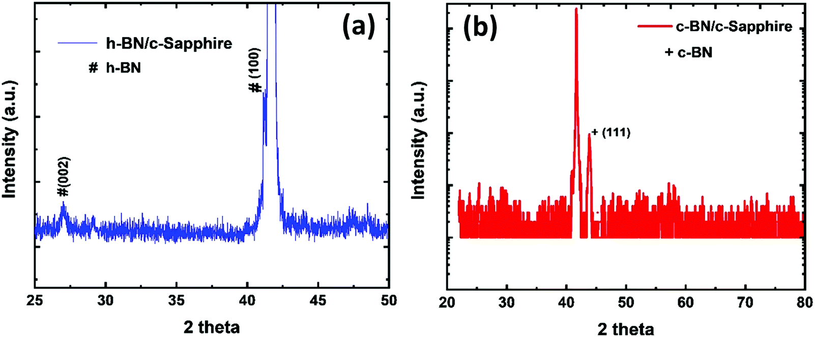 | ||
| Fig. 2 XRD pattern of (a) the as-deposited h-BN thin film on c-sapphire, and (b) the phase-pure c-BN thin film on c-sapphire after PLA treatment. | ||
Fig. 3 shows the Raman spectra of the as-deposited h-BN, phase mixture of h-BN and c-BN, and fully converted phase-pure c-BN after the laser annealing treatment. The Raman spectra are different for the samples annealed with different laser energy densities. To minimize the temperature variation effect on the measurements, we kept the laser power below 50 mW during the measurements.16 Because of the ionic nature of the zinc blende c-BN, the Raman active (Γ15) optical phonon mode at the center of the Brillouin zone splits into transverse optical (TO) and longitudinal optical (LO) phonon modes.17 These Raman active phonon modes show characteristic peaks at 1056 cm−1 (TO) and 1306 cm−1 (LO). A single first-order Raman active mode of Γ5 symmetry is present in h-BN at an energy of 1364 cm−1.17 The formation of the c-BN phase can be detected by the presence of the vibrational peak in the range of 1060–1100 cm−1 using infra-red (IR) spectroscopy. However, different compounds such as SiOx and some metal borides also show a similar type of absorption peaks in that same region. Therefore, we used Raman spectroscopy to conclusively identify the phase and assess the crystalline quality of the BN samples. It should be noted that the Raman analysis of the BN films is less affected compared to IR spectroscopy by factors such as film thickness, film–substrate interface, and optical properties of the substrate.18 It is always a big challenge to precisely determine the individual phase content in a mixed phase BN sample. Previous studies have used FTIR absorption peak intensities of h-BN (Ih-BN) and c-BN (Ic-BN) at wavenumbers ∼1080 cm−1 and 1380 cm−1, respectively, to calculate the cubic phase volume content by using the following expression: Xc-BN = Ic-BN/(Ic-BN + Ih-BN). However, this technique can only be implemented when the BN films are thin enough to provide an acceptable FTIR signal. Increasing film thickness introduces several complexities including: (i) the percent of transmittance drops close to zero and the c-BN absorption peak gets wider, (ii) the FTIR signal consists of nonlinear background due to the optical interference with thicker films, and (iii) large Reststrahlen bands form at higher wavenumbers due to the non-transmissible nature of the IR light between the LO and TO modes of c-BN through the c-BN lattice.19 Because of the considerably large film thickness (>0.5 μm) the FTIR spectroscopy is not preferable for analyzing the BN samples fabricated by the PLA technique. Therefore, we have chosen Raman spectroscopy to assess the quality and determine the c-BN phase content in the BN samples. The scattering efficiency of h-BN in Raman spectroscopy is several times higher than that of c-BN.20 Thus, during the assessment of the phase purity of c-BN films any trace of h-BN phase otherwise undetectable via other characterization techniques can easily be identified by Raman spectroscopy. One should also consider the relative scattering efficiency between the h-BN and c-BN Raman peaks to calculate the fraction of cubic phase content in the BN samples. The area intensities of the h-BN and c-BN peaks were corrected for discrepancy in scattering efficiencies. Reich et al.20 calculated scattering efficiency for c-BN and h-BN at different scattering wavelengths which have been considered during the calculation of the cubic phase content in the BN samples using peak fitting analysis. Raman spectroscopy is an established technique to determine the quality of the BN sample. Several studies have shown that the Raman peaks of c-BN samples substantially broadened and downshifted towards lower wavenumbers with the enhancement of defect states/density and decrease in crystal size.21,22 Therefore, it is difficult to obtain well-defined Raman spectra from c-BN films composed of small and highly defective crystallite entities. On the other hand, the Raman peaks are seen to be upshifted with compressive stress in the c-BN films.12 The observed upshifts in the Raman peaks of our samples with respect to the bulk c-BN (1055 cm−1 for TO and 1305 cm−1 for LO) coincide with the fact that compressively stressed c-BN films were fabricated by the PLA process.20 Additionally, the symmetry and smaller FWHM values of the Raman peaks obtained from the laser annealed c-BN samples imply improved crystallinity and better film quality.23 For reference we have compared the Raman spectra of our c-BN films obtained by the PLA process with three other Raman spectra: (i) c-BN crystals of size in-between 4 and 8 μm grown by the HPHT method (commercially from Showa-Denko Co. Ltd, Japan), (ii) c-BN samples grown by the dc jet plasma chemical vapor deposition (CVD) technique, and (iii) c-BN films deposited by physical vapor deposition (PVD) at low substrate bias (−35 V).24,25 The peak position and FWHM of both TO and LO Raman modes are shown for comparison in Table 1.
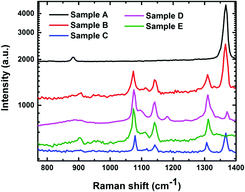 | ||
| Fig. 3 Raman spectra of the BN samples using a 532 nm green laser showing the characteristic E2g peak of phase-pure h-BN at 1370 cm−1, and characteristic LO(Γ), TO(Γ), and LO(L) peaks of c-BN at 1311.3 cm−1, 1073.1 cm−1 and 1140 cm−1, respectively. | ||
| Sample | Mode | Peak position (cm−1) | FWHM (cm−1) |
|---|---|---|---|
| HTHP 4–8 μm | TO | 1049.6 | 12.5 |
| LO | 1301.3 | 11.1 | |
| CVD | TO | 1048.4 | 28.8 |
| LO | 1301.8 | 19.7 | |
| PVD (−35 V substrate bias) | TO | 1058 | 60 |
| LO | — | — | |
| PLD and PLA (our experiment) | TO | 1073.1 | 10.2 |
| LO | 1311.3 | 9.1 |
In order to assess the feasibility of BN as an optoelectronic material in the UV range, it is important to understand the nature of the optical bandgap and accurately determine its magnitude. Despite the fact that h-BN and c-BN are the two most studied structures of BN, to date no agreement concerning their optical bandgap energy has been obtained experimentally. From the analysis of the available literature data it is evident that there is a considerable distribution in the experimentally obtained optical bandgap values ranging from 4.3 eV to 6.0 eV.26,27 On the other hand, in the case of pure c-BN the value of Eg was reported to be in-between 5.8 eV and 6.4 eV in the literature.17,28 Transmission measurements were performed in the visible and UV region to determine the optical bandgaps of our films. All the films are highly transparent in the visible region of the incident light spectrum. Fig. 4(a) shows the representative transmission spectrum of the phase-pure c-BN film. It is well established that h-BN is a direct bandgap semiconductor while c-BN is an indirect bandgap material. In the case of h-BN the value of p is 1/2 in the (αhν)pvs. Eg (Tauc) plot while p is equal to 2 for c-BN in the same plot due to the band to band transition. Therefore, sample A, which is predominantly composed of h-BN, is fitted well in the form of αhν = K1(hν − Eg)1/2 in the high energy region, where K1 is a material dependent constant. This plot is shown in Fig. 4(b). On the other hand, sample E, which is predominantly consisting of c-BN, is fitted well in the form of αhν = K1(hν − Eg)2, which is shown in Fig. 4(d). In all of the cases, the optical bandgap energy is calculated from the linear fitting profile of the x-axis intercept. The obtained direct bandgap energy from sample A was found to be 5.08 eV, whereas sample E corresponded to an indirect transition corresponding to 5.93 eV energy gap. Samples B, C, and D, however, consist of both h-BN and c-BN phase mixtures and therefore the data of these samples could not be directly fit well with either αhν = K1(hν − Eg)1/2 or αhν = K1(hν − Eg)2. Hence we followed a technique used by Davis in amorphous selenium29 to address this complexity by fitting the data of these three samples with αhν = K(hν − Eg) in the linear region, where K is a material dependent constant. Zhang et al.30 also followed the same procedure to determine the bandgap in BN films with different amounts of cubic phase content on Si and fused silica substrates. Fig. 4(c) represents the plots of αhν vs. Eg for samples B, C, and D. The X-axis intercepts from the fitted profiles of the linear regions give the bandgap energies of 5.63 eV, 5.79 eV, and 5.87 eV, respectively. In agreement with an effective medium approach, the optical bandgap of the BN samples with mixed phases should increase with increasing c-BN phase content. Fig. 5 represents the dependence of optical bandgap energy on c-BN phase content. In this plot, Eg increases steadily with c-BN phase content in the BN samples as both the phases present in the BN films have covalent bonding between B and N atoms. Therefore, we can introduce an empirical formula correlating the optical bandgap with the c-BN phase content from the linear fitting profile of this plot,
| Eg = Eh-BN × Ch-BN + Ec-BN × Cc-BN | (1) |
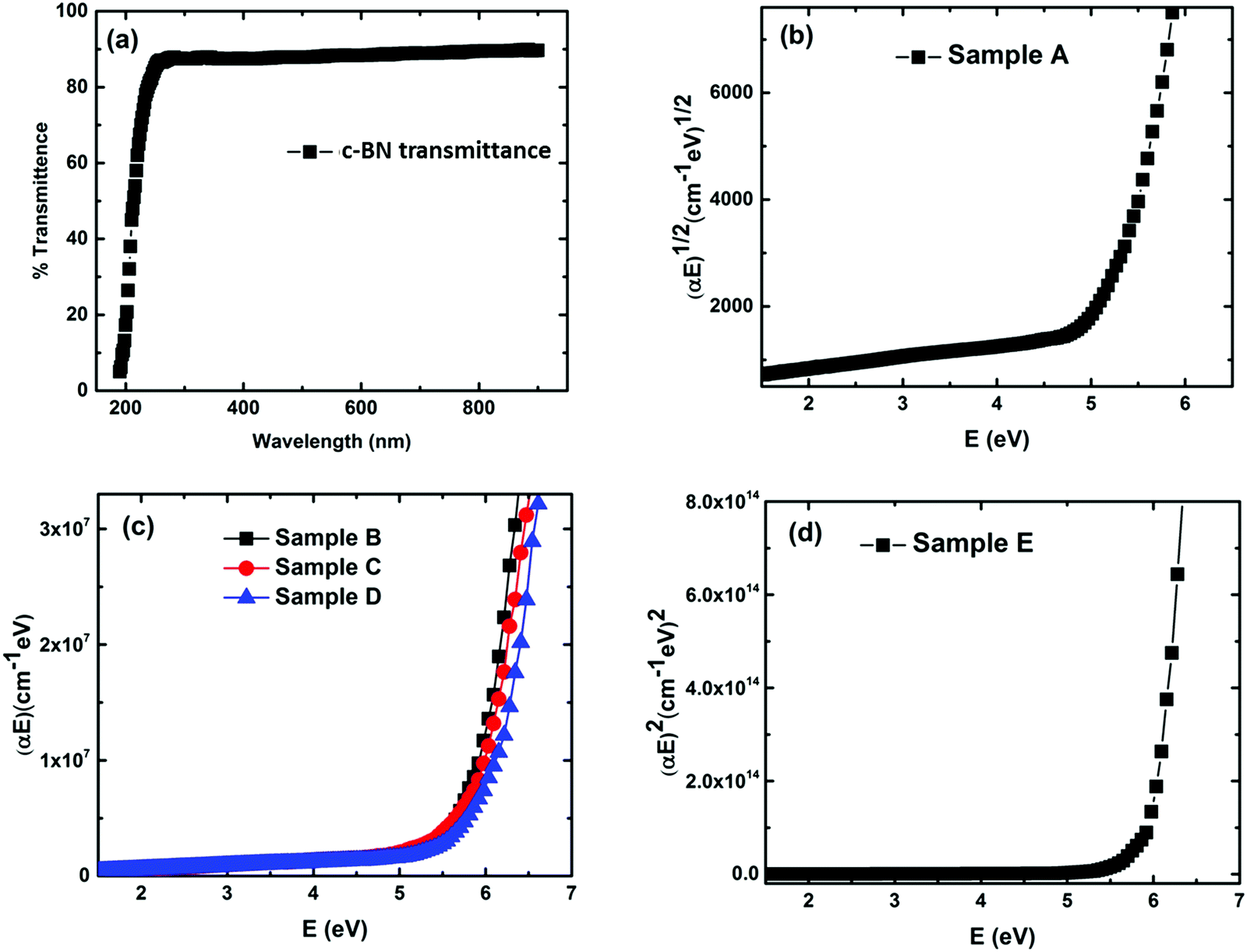 | ||
| Fig. 4 UV-Vis measurement plots of the BN samples. (a) Transmittance spectra of the phase-pure c-BN sample (sample E). (b) Tauc plot of phase-pure h-BN (sample A). (c) Tauc plot of samples B, C and D (mixed phases of h-BN and c-BN). (d) Tauc plot of phase-pure c-BN (sample E). | ||
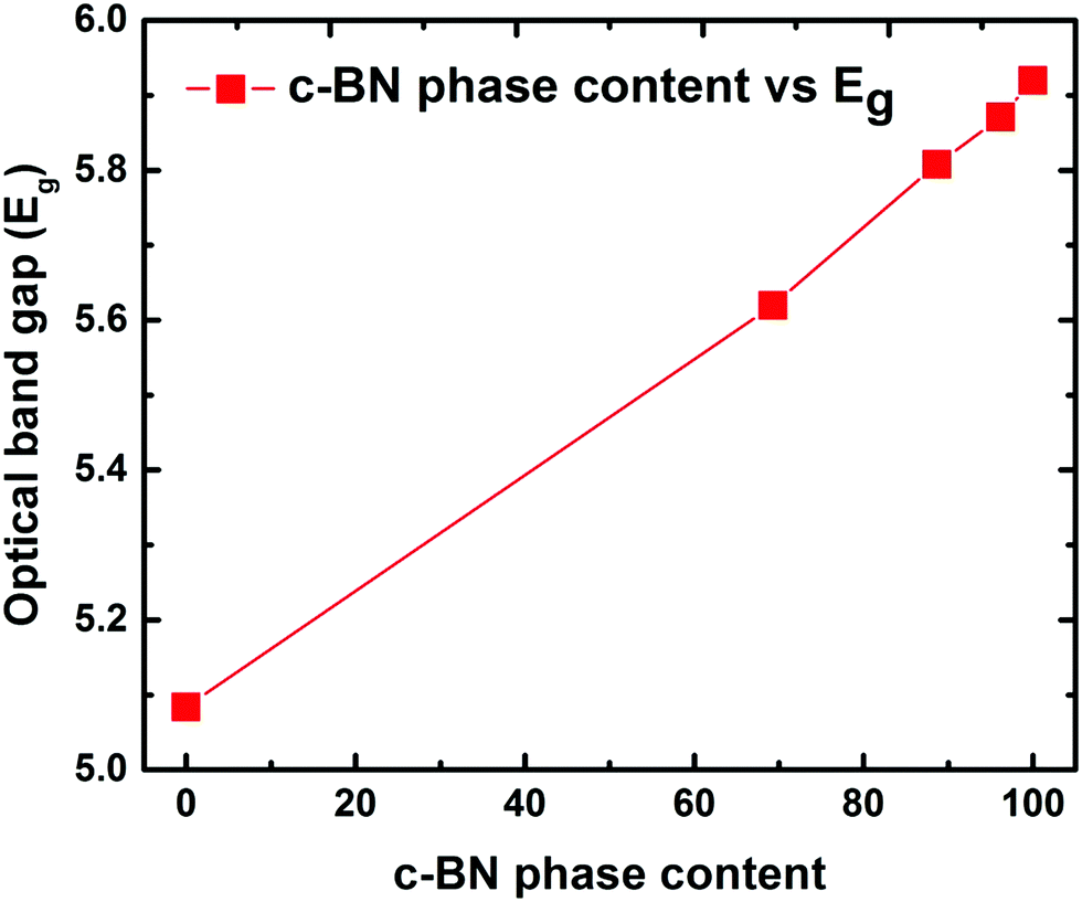 | ||
| Fig. 5 Optical bandgap vs. c-BN phase content showing the dependence of the obtained optical bandgap on the c-BN phase content. The increasing trend of the optical bandgap with the c-BN phase content gives the empirical formula (eqn (1)). | ||
In this experimental analysis we calculated the Eg of h-BN, c-BN and the phase mixture of h-BN and c-BN by assuming α as the energy dependent coefficient which varies as I(λ) = I0e−αt, where I0 is the intensity of the incident light at a particular wavelength (λ), I is the intensity of the transmitted light at that incident wavelength, and t is the thickness of the sample.34 The values of α have been derived successfully owing to the photon excitation from the relatively shallow acceptor states which lie 5.08 eV below the conduction band minimum in the case of h-BN. These acceptor states are thought to be distributed according to the Gaussian distribution profile and the density of states in the conduction band of h-BN varies in the form of (E − Eg)1/2, which signifies the parabolic profile of the conduction band.35 In the case of phase-pure c-BN the shallow acceptor states lie 5.93 eV below the conduction band minima. The band structures we considered to measure the optical bandgap energies for h-BN and c-BN perfectly match with theoretical band structures. The measured value of Eg for h-BN suggests a quasi-direct gap transition at H or K points.36–38 An Eg of 5.2 ± 0.2 eV, due to the direct transition at the H point (H3 → H2) of the Brillouin zone in the h-BN structure, reported by Hoffman and co-workers closely matches with our measured value of 5.04 eV.39 The Eg of c-BN can be correlated with the minimum Γ–X indirect energy transition of the theoretical studies.39 However, due to the unavailability of any theoretical study on the electronic structure and the optical energy bandgap calculations we cannot correlate the obtained Eg values of mixed phases of c-BN and h-BN.
Conclusions
The quality of the h-BN, phase-pure c-BN, and phase mixture of h-BN and c-BN thin films fabricated by our novel technique has been studied in terms of structural transformation and phase purity using a number of different characterization techniques. Raman spectroscopy has been successfully implemented to determine the phase purity and calculate the h-BN and c-BN phase contents in the mixed phase samples for the first time in BN films with relatively large film thickness. The structures of the BN samples were also confirmed consistently by UV-Vis measurements. A direct correlation between the phase fraction of h-BN and c-BN phase contents and the optical bandgap energy has been obtained in this experimental study. The mixed phase BN samples and the phase-pure c-BN films fabricated by this process can easily be doped with both p- and n-type dopants for optoelectronic applications. Overall, in this work a remarkable progress in the fabrication of high-quality phase-pure c-BN and a phase mixture of h-BN and c-BN has been made and these hold numerous possibilities in the field of electronics and optoelectronics under extreme environments and also this c-BN can successfully be implemented as a pivotal material for the machining of ferrous alloys to achieve prolonged life, reduced chemical reaction, and interfacial interactions.Conflicts of interest
There are no conflicts to declare.Acknowledgements
This research was supported by the Army Research Office Grant No. W911NF-16-1-0375. The authors would like to acknowledge the use of analytical instrument facility (AIF) at North Carolina State University, which is supported by the State of North Carolina and National Science Foundation. The authors are very pleased to thank John Prater and Siddharth Gupta for their technical assistance and useful feedback. We also wish to acknowledge the Fan Family Foundation Distinguished Chair Endowment for Professor J. Narayan.References
- F. R. Corrigan and F. P. Bundy, J. Chem. Phys., 1975, 63, 3812 CrossRef CAS.
- V. L. Solozhenko, High Press. Res., 1995, 13, 199 CrossRef.
- H. Neumann, Cryst. Res. Technol., 1995, 30, 910 CrossRef CAS.
- S. Ulrich, J. Schwan, W. Donner and H. Ehrhardt, Diamond Relat. Mater., 1996, 5, 548 CrossRef CAS.
- M. Lu, A. Bousetta, R. Sukach, A. Bensaoula, K. Walters, K. Eipers-Smith and A. Schultz, Appl. Phys. Lett., 1994, 64, 1514 CrossRef CAS.
- D. H. Berns and M. A. Cappelli, Appl. Phys. Lett., 1996, 68, 2711 CrossRef CAS.
- D. H. Berns and M. A. Cappelli, J. Mater. Res., 1997, 12, 2014 CrossRef CAS.
- X. W. Zhang, H.-G. Boyen, N. Deyneka, P. Ziemann, F. Banhart and M. Schreck, Nat. Mater., 2003, 2, 312 CrossRef CAS PubMed.
- J. Narayan and A. Bhaumik, APL Mater., 2016, 4, 020701 CrossRef.
- J. Narayan, A. Bhaumik and W. Xu, J. Appl. Phys., 2016, 119, 185302 CrossRef.
- J. Yu and S. Matsumoto, Diamond Relat. Mater., 2004, 13, 1704 CrossRef CAS.
- W. J. Zhang and S. Matsumoto, Phys. Rev. B: Condens. Matter Mater. Phys., 2001, 63, 073201 CrossRef.
- A. Haque and J. Narayan, Carbon, 2019, 150, 388–395 CrossRef CAS.
- V. L. Solozhenko, High Press. Res., 1995, 13, 199 CrossRef.
- R. K. Singh and J. Narayan, Phys. Rev. B: Condens. Matter Mater. Phys., 1990, 41, 8843 CrossRef PubMed.
- A. Haque, S. Gupta and J. Narayan, ACS Appl. Electron. Mater., 2020 Search PubMed.
- D. A. Evans, A. G. McGlynn, B. M. Towlson, M. Gunn, D. Jones, T. E. Jenkins, R. Winter and N. R. J. Poolton, J. Phys.: Condens. Matter, 2008, 20, 075233 CrossRef.
- P. B. Mirkarimi, K. F. McCarty and D. L. Medlin, Mater. Sci. Eng., R, 1997, 21, 47 CrossRef.
- G. Turrel, Infrared and Raman Spectra of Crystrals, Academic, London, 1972 Search PubMed.
- S. Reich, A. C. Ferrari, R. Arenal, A. Loiseau, I. Bello and J. Robertson, Phys. Rev. B: Condens. Matter Mater. Phys., 2005, 71, 205201 CrossRef.
- H. Saitoh and W. A. Yarbrough, Appl. Phys. Lett., 1991, 58, 2228 CrossRef CAS.
- T. Werninghaus, J. Hahn, F. Richter and D. R. T. Zahn, Appl. Phys. Lett., 1997, 70, 958 CrossRef CAS.
- A. Haque, P. Pant and J. Narayan, J. Cryst. Growth, 2018, 504, 17–25 CrossRef CAS.
- W. J. Zhang and S. Matsumoto, J. Mater. Res., 2001, 16, 3430 CrossRef CAS.
- K. M. Leung, H. Q. Li, Y. S. Zou, K. L. Ma, Y. M. Chong, Q. Ye, W. J. Zhang, S. T. Lee and I. Bello, Appl. Phys. Lett., 2006, 88, 241922 CrossRef.
- V. L. Solozhenko, A. G. Lazarenko, J.-P. Petitet and A. V. Kanaev, J. Phys. Chem. Solids, 2001, 62, 1331 CrossRef CAS.
- K. Watanabe, T. Taniguchi and H. Kanda, Nat. Mater., 2004, 3, 404 CrossRef CAS PubMed.
- V. Y. Kulikovsky, L. R. Shaginyan, V. M. Vereschaka and N. G. Hatynenko, Diamond Relat. Mater., 1995, 4, 113 CrossRef CAS.
- E. A. Davis, J. Non-Cryst. Solids, 1970, 4, 107 CrossRef CAS.
- X. W. Zhang, Y. J. Zou, B. Wang, X. M. Song, H. Yan, G. H. Chen and S. P. Wong, J. Mater. Sci., 2001, 36, 1957 CrossRef CAS.
- K. Yuge, A. Seko, Y. Koyama, F. Oba and I. Tanaka, Phys. Rev. B: Condens. Matter Mater. Phys., 2008, 77, 094121 CrossRef.
- J. Narayan, A. Bhaumik and A. Haque, Acta Mater., 2019, 178, 179–185 CrossRef CAS.
- J. Narayan, A. Bhaumik, S. Gupta, A. Haque and R. Sachan, Mater. Res. Lett., 2018, 6, 353 CrossRef CAS.
- F. N. Taufique, A. Haque, P. Karnati and K. Ghosh, J. Electron. Mater., 2018, 47(11), 6731–6745 CrossRef.
- D. A. Evans, A. G. McGlynn, B. M. Towlson, M. Gunn, D. Jones, T. E. Jenkins, R. Winter and N. R. J. Poolton, J. Phys.: Condens. Matter, 2008, 20, 075233 CrossRef.
- Y.-N. Xu and W. Y. Ching, Phys. Rev. B: Condens. Matter Mater. Phys., 1993, 48, 4335 CrossRef CAS PubMed.
- L. Liu, Y. P. Feng and Z. X. Shen, Phys. Rev. B: Condens. Matter Mater. Phys., 2003, 68, 104102 CrossRef.
- R. Dovesi, C. Pisani, C. Roetti and P. Dellarole, Phys. Rev. B: Condens. Matter Mater. Phys., 1981, 24, 4170 CrossRef CAS.
- D. M. Hoffman, G. L. Doll and P. C. Eklund, Phys. Rev. B: Condens. Matter Mater. Phys., 1984, 30, 6051 CrossRef CAS.
- A. Haque and J. Narayan, Stability of electron field emission in Q-carbon, MRS Commun., 2018, 8(3), 1343–1351 CrossRef CAS.
- A. Haque and J. Narayan, Diam. Relat. Mater., 2018, 86, 71–78 CrossRef CAS.
| This journal is © The Royal Society of Chemistry 2020 |