
 Open Access Article
 This Open Access Article is licensed under a Creative Commons Attribution-Non Commercial 3.0 Unported Licence
Engineering inclined orientations of piezoelectric films for integrated acoustofluidics and lab-on-a-chip operated in liquid environments
Yong-Qing
Fu
 *a,
Hua-Feng
Pang
ab,
Hamdi
Torun
a,
Ran
Tao
ac,
Glen
McHale
d,
Julien
Reboud
e,
Kai
Tao
f,
Jian
Zhou
g,
Jingting
Luo
c,
Desmond
Gibson
h,
Jikui
Luo
i and
PingAn
Hu
j
*a,
Hua-Feng
Pang
ab,
Hamdi
Torun
a,
Ran
Tao
ac,
Glen
McHale
d,
Julien
Reboud
e,
Kai
Tao
f,
Jian
Zhou
g,
Jingting
Luo
c,
Desmond
Gibson
h,
Jikui
Luo
i and
PingAn
Hu
j
aFaculty of Engineering and Environment, Northumbria University, Newcastle upon Tyne, NE1 8ST, UK. E-mail: richard.fu@northumbria.ac.uk
bDepartment of Applied Physics, College of Science, Xi'an University of Science and Technology, Xi'an, 710054, P. R. China
cShenzhen Key Laboratory of Advanced Thin Films and Applications, College of Physics and Energy, Shenzhen University, 518060, Shenzhen, P. R. China
dInstitute for Multiscale Thermofluids, School of Engineering, University of Edinburgh, Kings Buildings, Edinburgh EH9 3FB, UK
eDivision of Biomedical Engineering, James Watt School of Engineering, University of Glasgow, Glasgow, G12 8LT, UK
fKey Laboratory of Micro and Nano Systems for Aerospace, Ministry of Education, North Western Polytechnical University, Xi'an 710072, P. R. China
gCollege of Mechanical and Vehicle Engineering, Hunan University, Changsha 410082, P. R. China
hInstitute of Thin Films, Sensors & Imaging, University of the West of Scotland, Scottish Universities Physics Alliance, Paisley PA1 2BE, UK
iCollege of Information Science & Electronic Engineering, Zhejiang University, Hangzhou 310027, P. R. China
jSchool of Materials Science and Engineering, MOE Key Laboratory of Micro-Systems and Micro-Structures Manufacturing, Harbin Institute of Technology, Harbin 150001, P. R. China
First published on 23rd November 2020
Abstract
Different acoustic wave modes are required for effective implementation of biosensing and liquid actuation functions in an acoustic wave-based lab-on-a-chip. For efficient sensing in liquids, shear waves (either a thickness-shear bulk wave or a shear-horizontal surface acoustic wave) can achieve a high sensitivity, without significant loss of acoustic wave energy. On the other hand, longitudinal bulk waves or out-of-plane displacement waves (such as Rayleigh waves) enable efficient sampling functions and liquid manipulation. However, there are significant challenges in developing a lab-on-a-chip to efficiently generate multiple wave modes and perform both these functions on a single piezoelectric substrate, especially when a single crystalline orientation is available. This paper highlights the latest progress in the theories and techniques to deliver both sensing and microfluidic manipulation functions using engineered inclined-angled piezoelectric films, allowing for the simultaneous generation of longitudinal (or Rayleigh) and thickness-shear bulk (or shear-horizontal surface acoustic) waves. Challenges and theoretical constraints for generating various wave modes in the inclined films and techniques to efficiently produce inclined columnar and inclined crystalline piezoelectric films using sputtering deposition methods are presented. Applications of different wave modes in the inclined film-based lab-on-chips with multiple sensing and acoustofluidic functions are also discussed.
1. Introduction
Piezoelectric materials have the unique property of generating electricity when they are subjected to external deformation/pressure; and vice versa, they are able to perform actuation functions through geometrical changes when external electrical fields are applied. These materials include:1 (1) bulk crystals of quartz (SiO2), lithium tantalite (LiTaO3), lithium niobate (LiNbO3), sapphire (Al2O3), lead zirconate titanate (Pb(Zr,Ti)O3, PZT), barium strontium titanate (BaSrTiO3), etc.; (2) piezoelectric thin films such as PZT, zinc oxide (ZnO), aluminium nitride (AlN), LiNbO3, gallium nitride (GaN), and boron nitride (BN); and (3) piezo-polymers such as polyvinylidene fluoride (PVDF), polymer-ceramic composites, etc. By depositing metal electrodes on the top and bottom surfaces of a piezoelectric material, a bulk acoustic wave (BAW), in either a longitudinal mode or a thickness-shear mode (TSM), can be generated when electrical signals are applied to these two electrodes as illustrated in Fig. 1a and b. A common example is a quartz crystal microbalance (QCM), with a TSM wave mode generated in a quartz crystal sandwiched between two electrodes, which have been commercially used in various sensing applications. Film bulk acoustic resonators (FBARs, with a piezoelectric film on top of a membrane structure) and solidly mounted resonators (SMRs, with a piezoelectric film on stacks of alternate layers of low and high acoustic impedance forming a Bragg acoustic reflector) have recently been extensively studied. They have structures similar to those of BAW devices, but their dimensions (both size and film thickness) are much smaller (on the micron or sub-micron scale), thus achieving operation frequencies from sub-GHz to tens of GHz, suitable for high precision sensor applications.2,3 Similarly, FBARs and SMRs can have either longitudinal or TSM waves, similar to those shown in Fig. 1a and b, depending on the crystal orientation of the film.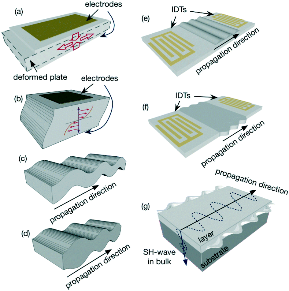 | ||
| Fig. 1 Illustrations of different types of commonly observed acoustic waves: (a) longitudinal bulk acoustic waves (BAWs) generated between a top electrode and bottom electrode; (b) thickness-shear mode (TSM) waves generated between two electrodes; (c) Lamb waves, antisymmetric mode (A mode, or flexural plate waves–FPWs); (d) Lamb waves, symmetrical mode or extensional mode (S mode); (e) Rayleigh surface acoustic waves (SAWs) generated on a piezoelectric material using interdigital transducers (IDTs); (f) shear horizontal SAWs (SH-SAWs) generated on piezoelectric materials using IDTs; (g) Love-mode waves generated on the surface of an SH-SAW device coated with a thin wave-guide layer. | ||
Lamb waves are commonly generated when the substrate thickness is smaller than or comparable to the wavelength of the propagating waves on the substrate (see Fig. 1c and d). Lamb waves include: antisymmetric mode (A mode), also called flexural plate waves (FPWs), and symmetrical mode or extensional mode (S mode). It has been recently reported that Lamb waves can be generated using thin film piezoelectrics on a membrane structure.4,5
In a surface wave configuration, interdigitated transducers (IDTs) are commonly deposited onto the piezoelectric material, and surface acoustic waves (SAWs) can be generated after resonant frequency signals are applied to these IDTs. The SAWs propagate on the surface of the material in either an out-of-plane (e.g. Rayleigh) mode or an in-plane (e.g., shear horizontal) mode, as shown in Fig. 1e and f. Rayleigh SAWs can be generated on specifically oriented bulk piezoelectric substrates such as ST cut and Y-cut quartz, 128° Y-X-cut LiNbO3 and X-112° Y-cut LiTaO3 substrates, as well as vertically aligned or (0002) oriented films (often called c-plane or z-plane orientated) of ZnO, AlN, PZT or LiNbO3. Shear-horizontal SAWs (SH-SAWs) are generated on ST-cut quartz, 64° Y-X-cut LiNbO3 and 36° Y-X-cut LiTaO3, and the waves propagate via a shear-horizontal mode on the substrate surface6,7 (Fig. 1f). SH-SAWs can also be generated on many piezoelectric thin films with in-plane textures such as (10![[1 with combining macron]](https://www.rsc.org/images/entities/char_0031_0304.gif) 0) (commonly called the m-plane) or (11
0) (commonly called the m-plane) or (11![[2 with combining macron]](https://www.rsc.org/images/entities/char_0032_0304.gif) 0) (commonly called the a-plane), or (102) orientations (commonly called the r-plane).8–19 Another commonly investigated SAW is Sezawa mode, which is excited in SAW devices that harbour a layered structure where the phase velocity of the SAWs in the substrate is much larger than that of the overlaid piezoelectric film.4,5 They are intrinsically guided waves, which propagate at the interfaces between the film and substrate. The ratio of the wavelength to the piezoelectric film thickness plays a critical role in the properties of Sezawa waves. As the waves propagate along the interface, the influence of the structure of the thin film may be limited, although the detailed effects have not been studied.
0) (commonly called the a-plane), or (102) orientations (commonly called the r-plane).8–19 Another commonly investigated SAW is Sezawa mode, which is excited in SAW devices that harbour a layered structure where the phase velocity of the SAWs in the substrate is much larger than that of the overlaid piezoelectric film.4,5 They are intrinsically guided waves, which propagate at the interfaces between the film and substrate. The ratio of the wavelength to the piezoelectric film thickness plays a critical role in the properties of Sezawa waves. As the waves propagate along the interface, the influence of the structure of the thin film may be limited, although the detailed effects have not been studied.
Generally, bulk piezoelectric materials are much thicker and have better piezoelectric parameters on a large scale, whereas piezoelectric thin films have advantages in microscale devices for MEMS and lab-on-chip applications.2–6 For a better understanding of the different film orientations of piezoelectric film materials, Fig. 2 shows four typically observed crystal orientations, i.e., (0001) c-plane, (100) m-plane, (110) a-plane and (102) r-plane. Love mode SAWs, one of the key guided acoustic waves,20 can be generated within a thin wave-guide layer (such as SiO2, ZnO or polymers with sub-micron thickness) coated onto an SH-SAW device as shown in Fig. 1g.21 The Love mode waves have been regarded as optimal for biosensing under liquid conditions, mainly because the acoustic velocity of the wave-guide layer is lower than that of the substrate; thus the SH-SAWs generated are mostly trapped within this thin wave-guide layer, leading to a high sensitivity to signal changes at the surface.22,23
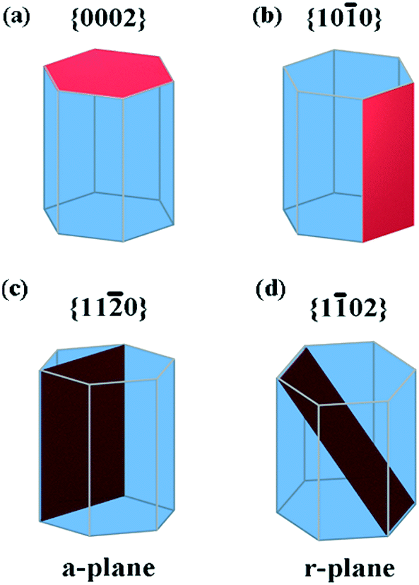 | ||
| Fig. 2 Illustrations of four commonly observed orientations for wurtzite piezoelectric crystal structures. (a) {0002} c-plane; (b) {100} m-plane; (c) {110} a-plane; and (d) {102} r-plane. | ||
Both the longitudinal bulk waves and out-of-plane (Rayleigh) SAWs are significantly damped when they come in contact with a liquid, because a large portion of their wave movements on the surface is vertical. Therefore, they are subjected to extensive damping, with significant deformations up to a few wavelengths at the solid–liquid interface. Therefore, they are not recommended for sensing applications in a liquid or highly humid environment, but instead have recently been extensively explored for acoustofluidic (or bio-sampling) functions such as mixing, jetting, nebulisations, particle/cell manipulations and acoustic heating.24–27 TSM waves, SH-SAWs and Love mode waves have been applied for liquid sensing due to their limited dissipation of wave energy during their propagations at the solid–liquid interface, but for the same reason, they are less commonly used in acoustofluidics.28,29
Recently acoustic wave devices have been extensively explored for detection of biomolecules, viruses, DNA, bacteria and cells.4,5,30 Most of these devices are required to work in a liquid environment. Therefore, there is a need to generate both shear waves (either TSM or SH-SAWs) for efficient bio-sensing and longitudinal or Rayleigh waves for bio-sampling and liquid sample manipulation processes, in one device platform. However, there are significant challenges to generate both these functions onto one single piezoelectric substrate with a given crystal orientation.
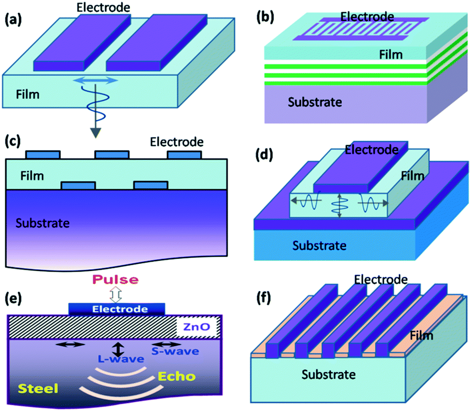
For the BAW devices, it is possible to generate both longitudinal and shear wave modes by fabricating devices on a bulk piezoelectric material with a suitably chosen crystal cut or orientation (e.g., non-vertically aligned ones). Similarly, thin-film FBARs based on specially designed inclined angled piezoelectric ZnO and AlN thin films have been extensively investigated to generate both longitudinal (for microfluidics) and BSM waves (for liquid sensing) and thus have been used under liquid conditions as shown in Fig. 3a.31–35 Generally the longitudinal wave has a higher frequency than the corresponding bulk shear mode due to their differences in acoustic wave velocities with an illustration shown in Fig. 3b.
 | ||
| Fig. 3 The configurations of thin films and acoustic waves that can be generated: (a) thin film FBARs with inclined angled piezoelectric thin films can generate both longitudinal (for microfluidics) and bulk shear waves (for liquid sensing); (b) a schematic illustration to indicate the differences in the frequencies of longitudinal and bulk shear waves; (c) Rayleigh SAW and SH-SAW generated with IDTs deposited on top of inclined angled piezoelectric films; (d) a schematic illustration to indicate the differences in the frequencies of Rayleigh SAW and SH-SAWs. | ||
For quartz-crystal based SAW devices, Rayleigh waves can be excited and then propagate along the X-cut direction on the 37° Y-cut quartz wafer, whereas the SH-SAW can be excited normal to the above direction. For thin film-based SAW devices, if the electrodes of the interdigitated transducers (IDTs) are deposited on top of inclined angled piezoelectric films as shown in Fig. 3c, both the Rayleigh SAW and SH-SAW can be generated. It is generally agreed that the SH-SAW has a higher frequency than the Rayleigh one as illustrated in Fig. 3d.36–39
Apart from using the inclined-angled or non-vertically aligned films, other potential methods have been proposed to generate waves for sensing under liquid conditions on vertically oriented (0002) materials or films. For example, one key and widely studied method is the use of a lateral field electrode (LFE) design40–43 as illustrated in Fig. 4a. This establishes laterally excited resonators to generate shear, or mostly pseudo-shear waves,44–47 which can be used for biosensing in a liquid environment, along with vertical waves for acoustofluidic functions to form an integrated lab-on-a-chip based on thin films.48 These types of LFE designs can be easily combined with FBAR or SMR designs, thus generating both longitudinal and shear thin film bulk modes.49 For the LFE mode, the shape, dimension and distance of two electrode pads are not critical, whereas the thickness of the piezoelectric material below is critical to determine the generation of the wave frequencies.
 | ||
| Fig. 4 The acoustic waves are excited in different structures: (a) lateral field electrode to form laterally excited ZnO or AlN thin film resonators to generate shear waves to be operated in a liquid solution; (b) tilt electric fields generated from standard IDTs on a c-axis vertically aligned piezoelectric film deposited on dielectric reflector stacks of AlN/SiO2, thus resulting in the electric fields being mainly aligned along the x-axis of the film plane; (c) the top and bottom electrodes are not perfectly aligned in the z-direction, thus the asymmetrical fields will generate both vertical and shear waves; (d) off-axis excitation, where the top electrode is relatively smaller than the bottom electrode; thus both pseudo-shear and pseudo-longitudinal waves can be generated; (e) both longitudinal wave (L-wave) and shear bulk wave (S-wave) generated in a standard pulse-echo ultrasonic test; (f) a periodically patterned ZnO film was deposited between fingers of IDTs to fill the gaps of the IDTs and implement SAW resonators. | ||
Another method is to modify electric fields generated from standard IDTs (as shown in Fig. 4b and c). In Fig. 4b, a bulk shear acoustic wave can be generated using a standard IDTs on a c-axis vertically aligned piezoelectric film deposited on dielectric reflector stacks of AlN/SiO2, thus resulting in the electric fields being mainly aligned along the x-axis of the film plane.50 Meanwhile, in Fig. 4c, the top and bottom electrodes are not perfectly aligned in the z-direction, thus the asymmetrical fields will generate both vertical and shear waves, although the film's crystal structure is vertically aligned.
Another method explored to a lesser extent is called off-axis excitation, where the top electrode is relatively smaller than the bottom electrode; thus both pseudo-shear and pseudo-longitudinal waves can be generated by this method as shown in Fig. 4d. A similar idea using two top electrodes with different areas has also been proposed for a ZnO SMR sensor, which can generate both shear and longitudinal modes for biosensing under liquid conditions.51 This design is actually often reported in standard pulse-echo ultrasonic tests where a mixture of shear and longitudinal waves can be easily generated when using a small area of the top electrode on thin-film coated metallic substrates (see Fig. 4e).52,53
There is another reported method54 in which a periodically patterned ZnO film was deposited between fingers of IDTs to fill their gaps and implement the SAW resonator as shown in Fig. 4f. Both the longitudinal and transverse wave modes can be generated.
However, the efficiency in generating strong and effective shear mode waves for all the above-mentioned unique designs is debatable.55,56
So far, the use of inclined angled thin films has been shown to generate both longitudinal (or Rayleigh waves) and TSM (or SH-SAW) waves. The produced inclined angled thin film devices can be used as the building blocks of integrated microsystems for microfluidic lab-on-a-chip, with the possibility of using separate wave modes for the functions of liquid transportation, biosampling and sensing. However, there are many contradictory views in the literature about the inclined angles of films (either columnar or crystal ones), the fundamental formation mechanisms of inclined crystals and their key growth parameters. Many different techniques have been developed but there are a lot of issues on uniformity of inclined angles, film thickness and acoustic wave properties. It is still a great challenge to successfully generate both these types of waves for SAW and FBAR devices and realise all the different functions of an integrated lab-on-a-chip. In this paper, we address all of the above issues and discuss the following key questions:
(1) What are the fundamental and theoretical issues in the use of inclined films to generate both vertical and shear waves?
(2) How can inclined columnar and inclined crystal piezoelectric films be produced efficiently using film deposition methods and what are the key processing parameters?
(3) How can both shear waves and longitudinal/Rayleigh waves be generated?
(4) How can these waves be effectively integrated into one platform and applied for lab-on-chip applications?
2. Fundamentals of angles of inclination and wave modes in inclined films
SAW and FBAR devices based on inclined films have recently been extensively studied and have shown improved mass sensitivities and good performance under liquid conditions.57,58 For these devices, the inclination angles have shown significant influences on the generation of acoustic wave modes.2.1. Definitions of three angles of inclination
Before discussing the details of these mixed wave modes, three different definitions of the angles of inclination must be clarified, which have been previously discussed in ref. 4 and 5: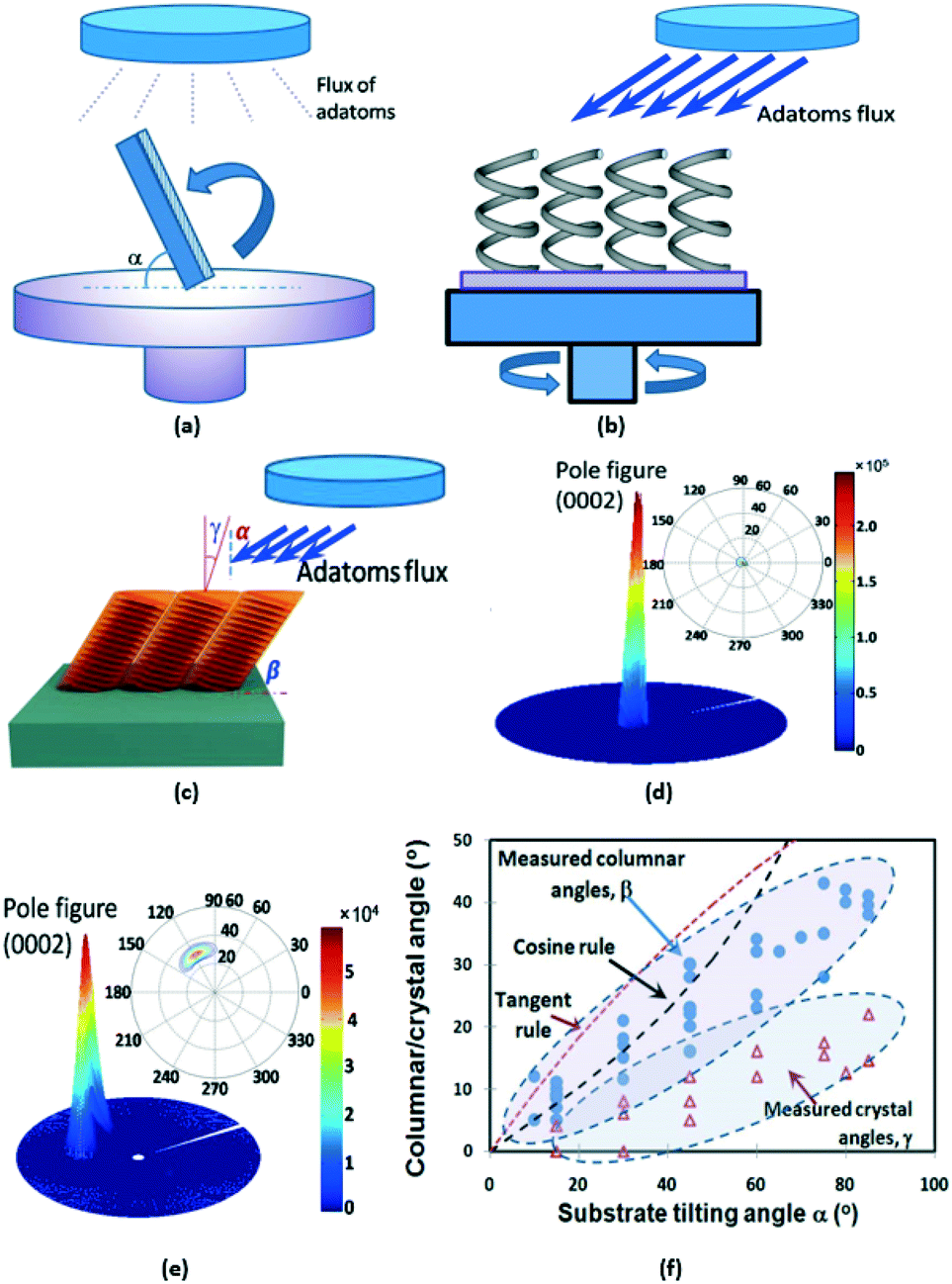 | ||
| Fig. 5 (a) Tilting angle deposition or oblique angle deposition (OAD); (b) glancing angle deposition (GLAD)with tilting/rotating in a 3D scheme at very large tilting angles; (c) illustration of the relationship between columnar tilting angles, substrate tilted angles and crystal tilting angles; crystal tilting angle obtained from (d) X-ray diffraction (XRD) pole figures of a c-axis orientated AlN film; (e) XRD pole figures of a 30° crystal inclined AlN film; both figures (d) and (e) are provided by Prof. Enrique Iborra from the University of Polytechnic Madrid, Spain; (f) different angle readings along with the data produced from the tangential and cosine rules.5 Here, the adatoms refer to the arriving and deposited atoms/ions onto the substrate surface, and they are derived from the sputtering targets through diffusion, migration and bombardment. | ||
Generally, the crystal inclination angle γ is much smaller than the columnar tilted angle β (see Fig. 5c and f). In many cases, even though the film shows a large columnar inclined angle, the crystal inclination angle is actually near zero, meaning that the crystals in the film still grow along the (0002) orientation.70 However in other cases, the cross-section morphology did not show any apparent inclined columnar morphology, even after the film was deposited by significant tilting of the substrate. However, detailed texture analysis using X-ray diffraction (XRD) revealed the formation of crystal inclined structures.71
2.2. Relationships among angles of inclination
Empirical relationships have been proposed to analyse the links between the substrate tilting angle α (or incident angle of the vapour flux) and columnar inclination angle β using the OAD method. For example, the tangent rule,72,73 cosine rule74,75 and other empirical equations are commonly used relationships:tan(α) = 2![[thin space (1/6-em)]](https://www.rsc.org/images/entities/char_2009.gif) tan(β) tan(β) | (1) |
| β = α − arcsin[(1 − cosα)/2] | (2) |
| tan(β) = 2tan(α)/{3[1 + ϕtan(α)sin(α)]} | (3) |
To the best of our knowledge, there are no available analytical relationships between the substrate tilting angle and crystal inclination angle (α vs. γ), or between the columnar inclination angle and crystal inclination angle (β vs. γ). This is mainly due to the crystal orientation/angles being influenced by a wide range of parameters, including process parameters, thin film material properties, target and substrate conditions and properties. Fig. 5(f) shows some data of crystal inclination angle γ as a function of substrate tilting angles α obtained from inclined angled ZnO and AlN films. Another challenge is that the XRD or TEM/EBSD methods are needed to precisely determine crystal orientations. However, these data are not widely available, partly because of the complexity of the geometry of the sample preparation and the speciality of the characterisation techniques. It is generally agreed that the crystal inclination angles are much smaller than the columnar angles, and in many cases, the c-axis crystal orientation (0002) is still dominant for most of the columnar inclined films. Another reason could be that the deposited “inclined” films are actually a mixture of vertically aligned crystals and inclined angled crystals, and it is difficult to develop mathematical models for the description of the relationships among the different angles (e.g., α, β and γ).
2.3. Key mechanisms determining columnar and crystal inclination angles
The columnar inclination angles are pre-dominantly controlled by deposition process parameters and substrate conditions. To generate columnar inclination angles in the films, the main controlling mechanisms include:(1) Direction and energy of the incoming adatoms on the deposited film;
(2) Surface micro-/nano-scale features and their shadowing and self-shadowing effects;
(3) Migration/diffusion of surface adatoms;
(4) Channelling effect or momentum/bombardment of arriving adatoms.
On the other hand, crystal inclination angles γ in the deposited films are intrinsically determined by competing factors among the growth rates of different crystal orientations or crystal planes on the film surface,77,78 which are controlled not only by process parameters, but also by material properties of both the film and the substrate. In the following, we will discuss a few key factors.
• Shadowing effect (mostly determines the columnar inclined angles).
During the OAD processes, the newly generated crystal nuclei on the substrate can form shadows behind them, which prevents the further formation of microstructures in these “shadowed” regions (see Fig. 6a), thus forming columnar inclined angle structures. This so-called shadowing effect is strongly linked to the directionality of the incoming particles. The inclined angled columnar structure is easily generated when the arriving particles have a good line of sight such as in an evaporation process, and also if the substrate tilted angle is large enough. On the contrary, during the sputtering process, the plasma contains energetically charged ions, reactive species and sputtered atoms, which are all attracted onto the surface of the deposited film with different impinging angles. There is a well-known cosine law to describe the distribution of the sputtered adatoms as below (also illustrated in Fig. 6b):79
| J(θ) = Yφ(cosθπ) | (4) |
 | ||
| Fig. 6 (a) Illustration of the shadowing effect during film deposition; (b) cosine law distribution of the sputtered adatoms on the substrate surface; (c) channelling effects during the sputtering process; (d) a circular-shaped target produces a ring distribution of inclined columnar angles (dark area) in the films, which can be revealed clearly from the illustration of the cross-section morphology; (e) an interlayer can promote the growth of inclined angled films; (f) pre-treatment of the surface to generate the desired surface roughness or surface topography and enhance the shadowing effect for growth of inclined angled films; (g) an additional blind/shutter positioned between the target and the substrates can change the plasma distribution onto the deposited films, thus promoting the inclined film growth; (h) an external oxygen or nitrogen ion or plasma source can control the oxygen/nitrogen ion bombardment to the deposited film during its inclined angled film growth. | ||
• Bombardment and channelling effects (for both columnar and crystal inclination angles).
During sputtering processes of ZnO, AlN and PZT films, various reactive species (such as O–, O, N, N+, N2+, etc.) and energetic species (such as Ar or Ar+ ions) in the plasma have strong influences on the energy transfer to the deposited films. During a standard magnetron sputtering process, the kinetic energy of sputtered atoms/ions arriving at the substrate could vary from sub-eV to hundreds of eV, which generate various effects (such as deposition, bombardment, etching, and implantation) and have a significant effect on the formation of columnar structures. As will be explained later, process parameters, such as a higher plasma power or a lower pressure, will result in an increase of the kinetic energy of these impinging atoms onto the substrate, which is one of the key reasons why fully crystalline films and also piezoelectric effects of ZnO, AlN and PZT can be easily achieved in the sputtering process operated without any external heating, or post-poling processes.4,5 Similarly, this effect would significantly influence the columnar inclined angles of the deposited film.
It is well-known that bombardment of the adatoms during sputtering will generate the so-called channelling effects (see Fig. 6c), which enhance the formation of columnar inclined structures, especially at a low incident flux and in a low temperature/pressure environment. In such circumstances, free movement of adatoms (deposited onto the substrate surfaces) can be restricted in a certain direction, thus promoting film growth along a desired orientation. For example, the (100) plane was found to be easily generated when the film was exposed to ion irradiation during electron beam evaporation due to its line-of-sight effect.80 During deposition of ZnO and AlN films, the film texture was changed from (0002) into (100) or (110) by using a directional oxygen or nitrogen ion beam placed at an angle to the substrate surface, which is mainly due to this ion channelling effect.81
• Surface migration/diffusion (for both columnar and crystal inclination angles).
Irradiation or bombardment of the arriving adatoms could contribute to the densification of the film's microstructure by enhancing the mobility of the deposited adatoms through the angular distribution of the neutral species.82 During the sputtering process, ion bombardment (mainly Ar, as well as O2 or N2) will significantly influence the structures of the crystals, as well as the development of large compressive stress,83,84 and could result in either formation of dense microstructures (due to the enhanced mobility of the deposited adatoms), or porous structures (due to the channelling effect or bombarding/damaging effects). In many cases, significant surface migration of adatoms deposited onto the film surface is not effective to promote the crystal inclined angle formation.
• Nature of the film material and bonding probability (mostly for crystal inclination angles).
Crystal angles of films are linked with the nature of film materials and also different bonding probabilities of atoms during growth. For example, for an AlN film, this factor could link to the formation of bonds such as (N, Al) or dimers (Al–N).85 It was reported that a higher chamber pressure promotes the generation of more (Al–N) dimers thus resulting in the growth of AlN (100) planes. Meanwhile, at a low pressure, atoms of N and Al are dominant, rather than the dimers of Al–N, and thus the (0002) growth is promoted.73 The effects of pressure will be discussed in the next section.
2.4. Effects of sputter deposition process parameters
As discussed above about the physical mechanisms, the energy/angular distribution of the incoming material flux and the mobility of the adatoms during the inclined angled deposition process are critical for the formation of film microstructures. All sputter deposition process parameters will influence the film growth in different orientations and the surface mobility of adatoms and thus will influence the inclination angle of the film growth.76 These key process parameters include:4,5 the nature of the substrate (such as phases or chemical composition, crystalline orientation, roughness, etc.) and process parameters (such as gas pressure, target plasma power, position and distance of the substrate vs. target, deposition time, bias potential, substrate temperature, gas ratio and flow rates, external ion/electron beam source, and plasma shields).86When an external bias voltage/power source is applied to the substrates during the sputtering deposition, the film orientation along (0002) is generally enhanced, but not the other orientations due to the normal direction of the energetic Ar ions bombarding onto the substrate surface. During the growth of ZnO and AlN films, a positive bias has been shown to increase the kinetic energies of oxygen or nitrogen ions, and enhance the mobility of adatoms arriving onto the film surface, causing significant bombardment/cleaning effects, large compressive stress and increase in roughness. A negative bias decreases bombardment but still provides sufficient mobility of adatoms arriving onto the film surface, thus enhancing (0002) texture growth.4,5
O2/Ar or N2/Ar gas ratios also have significant effects on the film texture.93 For example, AlN films with (100) or (110) orientation were obtained on 3C-SiC-on-Si substrates by simply increasing the nitrogen to argon ratio from 40% to 80% at a total gas flow of 50 sccm.84 In this case, the variations of the gas ratio would change the kinetic energy of the atoms deposited onto the films.
0)//LaAlO3(100),101 ZnO(110)/r-plane (102),102 and ZnO(110)/sapphire Al2O3(012).103 However, these epitaxial growth methods are expensive and the orientations are significantly dependent on the quality of the substrate materials and deposition conditions.16,103
Another commonly used method for changing the film orientation is to deposit an interlayer or a seed-layer (as illustrated in Fig. 6e), which could provide a template and promote the inclined angle growth of the piezoelectric films.104,105 For example, a thin AlN buffer of tens of nanometres has significantly facilitated the crystal quality of a-pane ZnO films and the formation of SH-SAWs.106 This type of interlayer does not need to be a piezoelectric material. This interlayer can be further pre-treated to generate the desired surface roughness or surface topography and enhance the shadowing effect in order to grow columnar inclined angled films (see Fig. 6f for some examples of these patterns). For example, a ZnO film with an inclined angle of 45° was obtained on a diamond substrate107 with pre-deposited pyramidal-shaped diamond features,108 mainly due to shadowing effects. Pre-patterned substrates can be prepared using a variety of methods, including photolithography, ion-beam milling, laser beam writing, nano-imprinting, embossing and self-assembly of nano-structured array patterns.
3. Sputtering techniques and technical challenges
In this section, we will discuss further about the sputtering techniques and challenges to realise different types of inclined films.3.1. Substrate tilting or target tilting
As mentioned, inclined ZnO and AlN films are commonly prepared using the OAD method.81,109–114 The setup and process of the OAD method are simple, through either tilting the substrates, or sometimes tilting the target. However, the uniformity is critical, and the inclination angles and film thicknesses could be dramatically different along the substrate plane, which causes a big problem for massive production and device performance. Also nanorods or helical structures of ZnO or AlN can easily be grown using the OAD or GLAD method. However, high-performance SAW and FBAR devices have not been generated from these highly porous nanostructures, due to high dissipation of energy for effective wave propagation.3.2. Locating samples at off-centre positions115
In the sputtering process, if the target is small compared with the substrate, a deposited film has a vertically columnar structure and (0002) orientation at its centre area as shown in Fig. 6d as an example. At a certain distance away from the target (or at off-centre positions from the plasma source as shown in Fig. 6d), inclined angle columnar structures with tilted angles up to 10° to 20° can be obtained, mainly due to ion channelling and shadowing effects.116 However, at locations far away from the plasma source, the (0002) orientation becomes dominant again as illustrated in Fig. 6d, mainly due to the limited ion/electron/adatom bombardment energy and insignificant channelling effects, leading to the dominant self-orientation along the (0002) orientation. This simple technique is believed to avoid the need for any special re-configuration of the deposition setup. However, the window area over which a uniformly inclined angle is produced is quite small (for example, a circular and ring area as shown in the dark area in Fig. 6d). This surely poses a challenge for the mass production of acoustic wave devices.3.3. Epitaxial growth on a specific substrate
Generally, by selecting a suitable substrate with a preferred orientation, inclined crystal films can be deposited using specific methods. However, these process methods are generally expensive, complicated, and difficult to control, as already discussed in section 2.4.5.3.4. A suitable seed layer with inclined angles
Inclined films can be obtained when they are grown onto a pre-deposited seed layer with a texture or pre-fixed inclined angle on the substrate. For example, using a textured Al film as a seed layer, tilted crystal ZnO films have been developed for liquid sensors.108 Using an AlN (29) orientation seed layer, inclined angled ZnO films with a c-axis crystal inclined at angles up to 45° have also been successfully obtained. The inclined crystal AlN seed layer enhanced the coupling coefficients of the ZnO films and achieved narrower angle distributions in the inclined crystal film.117–120 Technically this (29) AlN seed layer could be obtained using a sputtering method with a low sputtering power and a relatively high pressure.120 More details have also been discussed in section 2.4.5.
3.5. Using a shutter or blind placed between the target and substrate
An additional blind/shutter (for example, a metallic plate) can be placed between the target and the substrates and thus only allows oblique particles to arrive on the substrate surface (see Fig. 6g).121 The changes of plasma distribution near the shutter or blind enhance the ion bombardment/channelling and shadowing effects.122 This type of blind shutter can also be designed to move horizontally or rotated into different tilting angles, thus the distributions of plasma onto the substrate would be changed, thus realising different columnar angled films. However, the obtained area is relatively small and the uniformity of inclined angled films is often poor.3.6. External ion or electron beam sources
An external oxygen or nitrogen ion beam source can be used to control the oxygen/nitrogen ion bombardment during film growth as illustrated in Fig. 6h.123 These sources, including an ion beam, an external electric field,124 or an additional anode located near the substrate, can have a significant effect on the orientation of the growing films based on ion channelling effects,37 as discussed in section 2.4.1. This generally makes the deposition process complicated and high cost, and the treated area of the film is not large, which is mainly dependent on the size of ion beam sources.3.7. Summary of technical challenges
Even though inclined angled films as thick as a few microns (see Fig. 7(a) for an example) with a size of a four inch wafer have been successfully prepared using different techniques during the sputtering deposition, there are still many critical issues to be solved: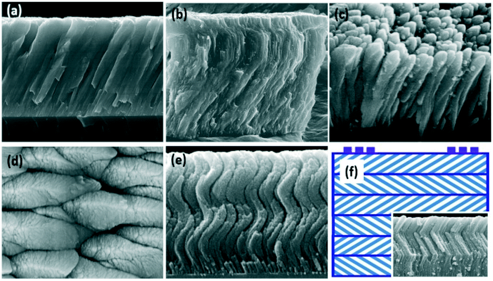 | ||
| Fig. 7 (a) Inclined angled ZnO films with a thickness of 3.5 microns on silicon; (b) the columnar inclination angle of films has gradually changed during deposition; (c) porous and loose columnar inclined microstructures; (d) rough and significantly elongated surface grainy structures for columnar inclined angled ZnO films; (e) example of 3D spiral and porous titania nanorod structures fabricated from the GLAD method; (f) illustration and example of multi-layered zig-zag ZnO structures. | ||
(1) Non-uniformity of film thickness and inclination or tilting angles over a large planar scale. As mentioned, most of the methods used to generate the inclination angle are not able to obtain a significant uniformity over large areas (for example, larger than 2 or 3 inches);125
(2) Variation of inclination angles along the film's cross-section (e.g., thickness) direction. It is a challenge to maintain a constant inclined angle along the thickness direction. Studies showed that the columnar inclination angles of films would often be gradually changed during deposition, or sometimes even change to a vertical orientation during deposition (see Fig. 7b for an example).81,126 These phenomena can be explained by the inevitable minor changes in the deposition conditions occurring over a lengthy deposition process (in most cases tens of hours), which could change the mobility of deposited species.
(3) Significant variations in acoustic wave propagation characteristics in planar directions. The large variation in c-axis tilt angles over a large area causes difficulties in obtaining consistent resonant frequencies and repeatable performance when a number of resonator chips are fabricated over this area. The acoustic wave velocities and frequencies of the devices decrease with increasing angles of inclination.
(4) A mixture of c-axis and inclined crystals in the deposited film. It is commonly seen that for the prepared inclined films, XRD analysis reveals that the film actually consists of both c-axis and crystal inclined films. This is probably the reason why many characterisation data of crystal inclined angles are confusing. However, identification of the precise percentages or ratios between them would be a challenging work.
(5) Formation of loosely columnar, porous or nanofiber structures due to self-shadowing effects. When the film is deposited at very large substrate tilting angles (e.g., above 60° or 70°), the formed columnar microstructures are normally quite porous and loose (see Fig. 7(c)), and many film surfaces are very rough with a significantly elongated grainy surface morphology (see Fig. 7(d)). Indeed, both the OAD and GLAD methods have been mainly used to generate nano-pillars, nanorods or 3D spiral porous structures (see Fig. 7(e) for an example). Tait127 derived an equation about the density of the film, ρ, as a function of the substrate tilting angle, α.
| ρ = 2cosα/(1 + cosα) | (5) |
It should also be noted that one of the key advantages using piezoelectric films for acoustic wave devices is the generation of in-plane isotropic acoustic wave properties,4,5 so the patterning positions or directions of IDTs or electrodes will not affect the wave mode generation and acoustic wave properties (such as velocities or frequencies). However, if columnar and crystal inclined films are used, the anisotropic acoustic wave properties within the film plane negate this benefit, e.g., becoming significantly anisotropic.
(6) Poor film adhesion for porous and nano-columnar structured films at large inclination angles. Highly inclined columnar angled films generally do not have as good adhesion as vertical and dense films, although the film stress could be decreased significantly at a larger columnar tilting angle.129 The lower film stress is mainly due to the formation of defects which cause tensile stress and are compensated for by film compressive stress.
In order to solve the issue of poor thickness uniformity, zig-zag (or spiral) patterns have been prepared by repeatedly changing the tilting angles of substrates (or by rotating the substrates) during tilted angle deposition.129–133 By using multi-layered zig-zag structures as shown in Fig. 7f, the longitudinal mode was found to be significantly suppressed, whereas the shear mode was not affected.130 The operational frequency and absolute sensing sensitivity in the liquid have also been reported to increase with layer numbers.132 This means that the FBAR or SAW devices made of these multi-layered zig-zag films should significantly enhance the performance of the shear waves. The uniformity of the thickness of inclined films could also be improved if compared with one single inclined film.131,134 Although in principle, this zig-zag film can be easily achieved using OAD and GLAD methods, the process increases the complexity of wave mode generation and device fabrication, and the microstructures become much poorer whilst the surface roughness is increased dramatically, all combining to pose significant challenges for its applications.
4. Effects of the inclination angle on wave propagation
4.1. On thin film bulk acoustic waves
Inclination angles (both columnar and crystal lattice) have significant effects on peak amplitude ratios between shear and longitudinal wave modes and their electromechanical coupling coefficients.134 However, it should be noted that for most theoretical studies, the crystal inclined angle γ was used in the analysis, whereas for most of the experimental studies, the columnar inclined angle β was often used in the data analysis.Fig. 8a and b show the theoretical values of wave velocities of both longitudinal and bulk shear modes of an AlN film as a function of crystal inclined angles, respectively, which follows the results proposed in ref. 134. As shown in Fig. 8a, the velocity of longitudinal wave decreases quickly with the increase of the inclination angle to ∼45°, above which it increases slightly until 90°. Meanwhile, as shown in Fig. 8a, the velocity of bulk shear waves increases continuously with the increase of the inclination angle to 35°, above which it gradually decreases until 90°. Fig. 8b shows the electromechanical coupling coefficients of the AlN film as a function of the c-axis inclination angle for the bulk acoustic waves (including FBARs). When the inclination angle is increased from 0 to 45°, the ratio of shear wave mode (to the longitudinal one) and its k2 values gradually increase, whereas those of the longitudinal mode gradually decrease. The values of k2 for the shear and longitudinal waves become similar at an angle of ∼10°. The k2 values of the shear mode become larger than the longitudinal values with the angle increased from ∼10° to ∼60°.135–137 The maximum k2 value of shear mode resonance occurs at a c-axis angle of inclination of about 25–38°. Theoretical analysis shows that pure thickness-longitudinal modes for ZnO (or AlN) FBARs are generated at c-axis angles of 0° (0°) and 67.1° (65.4°), whereas pure thickness-shear modes for ZnO (or AlN) FBARs are generated at 43° (46.1°) and 90° (90°).134,138
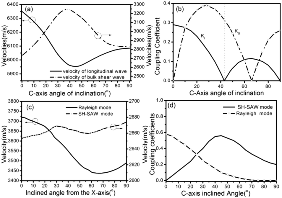 | ||
| Fig. 8 (a) Theoretically calculated wave velocities between longitudinal and bulk shear modes; (b) electromechanical coupling coefficients for both shear and longitudinal modes as a function of c-axis inclined angles for the FBAR devices; figures are redrawn and modified based on the results from ref. 134 and 138; (c) theoretically calculated wave velocities between Rayleigh and SH-SAW modes; (d) electromechanical coupling coefficients for both Rayleigh and SH-SAW modes as a function of c-axis inclined angles for the SAW devices. Figures are redrawn and modified based on the results from ref. 139, 140 and 143. | ||
Pang et al. studied the effect of inclination angles using a pulse-echo ultrasonic method141,142 for inclined ZnO films with different columnar inclination angles on steel substrates. Results showed that both the longitudinal echoes and shear echoes from the back wall of the steel plate could be obtained. A dual mode wave pattern (i.e., with both components of longitudinal and shear waves, mainly due to the small size of the top electrode compared to that of the metal substrate) was detected for the ZnO film with a crystal inclined angle of 0°. When the inclined columnar angle was increased, the amplitude ratios of the shear/longitudinal wave components were increased. When the inclined angle was increased to 31°, a nearly pure shear wave was obtained whilst the longitudinal wave excitation was significantly suppressed.141 For further increases of the inclination angle up to 35°, the shear wave was still dominant but the longitudinal component re-appeared.141
4.2. On SAWs
Reports on the effects of the inclination angle on the generation of Rayleigh mode and SH-SAWs are less readily available. This is mainly because a relatively thicker inclined film with a larger scale of uniform inclination angle is required for the generation of these SAW modes, and the IDTs for the SAW devices generally have larger sizes (for example, in many cases the dimensions of their reflectors are added). Fig. 8c shows the velocity results of Rayleigh and SH-SAW modes as a function of the inclined angle vs. X-axis in bulk LiNbO3 SAW devices. When the inclined angle is increased from 0° to 90°, the theoretically calculated velocity of the Rayleigh mode is much lower than that of the SH-SAW mode.139,140 A similar dispersive behaviour of the Rayleigh and SH-SAW modes exists in the inclined piezoelectric films.136Fig. 8d illustrates that when the crystal inclined angle γ is 0° (e.g., (0002) orientation) for the ZnO SAW devices, the Rayleigh wave is dominant and has the largest value of k2. With an increase in crystal inclined angle γ, the value of k2 for the Rayleigh wave gradually decreases until becoming negligible as the crystal inclined angle approaches 90°.143 Conversely, the amplitude ratio and k2 value of the SH-SAW peak become zero for vertically aligned films, but they increase with the crystal inclined angles up to 45°, and then gradually decrease up to 90°.Yanagitani and Suzuki144 reported that c-axis inclined AlN films showed significant decreases in shear wave acoustic impedance, but not in that of the vertical Raleigh type of waves. They have attributed this effect to the significant shear elastic softening caused by the weak inter-columnar connection. This elastic softening effect could also explain the difficulties in achieving the SH-SAWs in inclined films, and there are few papers about the successful generation of both wave modes in inclined films.
5. Sensing, acoustofluidics and integrated lab-on-a-chip using inclined films
5.1. FBAR liquid sensors and microfluidic devices based on inclined angled films
Recently, FBAR or SMR sensors with inclined angled piezoelectric films have been extensively studied for biosensing in liquid. These sensors could be made from both ZnO and/or AlN films with columnar inclination angles and crystal inclination angles to generate shear waves for sensing in liquid.144–148 The inclined angled films used in the fabrication of the FBAR or SMR devices are easily obtained as they are generally very thin (sub-microns to one or two microns) and small (e.g., micron scale). Within such a thickness range and such an area range, a uniform inclined angled film in both thickness and planar directions is readily obtained, enabling a huge number of successful reports on their applications. Both ZnO and AlN films have been extensively used in these FBAR or SMR devices for biological applications in liquid environments as summarized in Table 1. Due to their much higher wave propagation velocities for AlN films compared with those for ZnO films, AlN FBARs or SMRs have their advantages compared with those of ZnO devices, but the ZnO film has its advantages with relatively higher electro-coupling coefficients.149 To further enhance the sensitivity and performance of FBAR devices, new materials, such as carbon nanotubes and graphene, were also deposited onto the inclined AlN film.150| Piezoelectric materials | Structures | Inclined angle | Working frequency | Sensitivity | Key applications | Ref. |
|---|---|---|---|---|---|---|
| ZnO | FBAR | 2 GHz | 2.4 kHz cm2 ng−1 | Detect DNA and protein molecules | 151 | |
| ZnO | FBAR | 16° | 830 MHz | 1 kHz cm2 ng−1 | Water–glycerol solution | 152 |
| ZnO | FBAR | 1.04 GHz | 500–1358 Hz cm2 ng−1 | Blood proteins (e.g. A1b, IgG and fibrinogen) | 153 | |
| ZnO | SMR | C-axis inclination angle 25° | 1.1 GHz | 4.9 kHz cm2 ng−1 | Rabbit immunoglobin G (IgG) molecule | 104 |
| ZnO | FBAR | 1.4 GHz | Human blood coagulation process | 154–156 | ||
| ZnO | FBAR | 800 MHz | 50 ppm | CO2 | 157 | |
| ZnO | 13.6° tilted c-axis | 1.28 GHz | 158 | |||
| ZnO | FBAR | c-axis inclined angle of 24° | 2.26 GHz | 20 pg ml−1 | Cardiac biomarkers in the clinical serum | 159 |
| AlN | FBAR | c-axis 23° | 800 Hz cm2 ng−1 | Human IgE | 160 | |
| AlN | FBAR | 30° | 700 MHz to 1.5 GHz | 1.5 to 2.9 kHz cm2 ng−1 | Streptavidin and biotinylated BSA, and crosslinked fibrinogen | 161, 162 |
| AlN | SMR | Crystal inclined angle of 30° | 1.2 GHz | 163 | ||
| AlN | FBAR | 20° columnar inclined | 1.2 GHz | 2045.89 Hz cm2 ng−1 | Carcinoembryonic antigens (CEA) | 164 |
| FBAR | 23°-Tilted columnar structure | 1.175 GHz | 1.425 × 105 cm2 g−1 | IgE | 165 | |
| AlN | FBAR | Inclined angles of 23° | 1.17 GHz and 2.07 GHz | 2295 Hz cm2 ng−1, and 1363 Hz cm2 ng−1 | 166 | |
| AlN | Shear mode SMR | 1.3 GHz | 1800 kHz pg−1 cm−2 | Gravimetric biosensor | 57 | |
| AlN | FBAR | 21.6° crystal inclined | 1.87 GHz (6221 m s−1) and 3.15 GHz (10268 m s−1) |
Human haemostatic parameters, such as prothrombin time (PT) | 167, 168 |
As discussed above, inclined angled FBAR devices have been widely used in liquid biosensing, whereas so far, there are no reports for liquid actuation applications using the inclined angled FBAR devices. The integrated functions for both microfluidics and biosensing on one platform have never been demonstrated. In principle, bulk acoustic waves are able to generate liquid streaming and create flow patterns. For example, a circularly self-focused bulk wave acoustic transducer capable of generating focused waves on a (0002) oriented ZnO film on silicon, so-called “liquid needles”, was used to generate a focused acoustic wave in a liquid chamber and to produce a needle-shape liquid column on the free surface of the liquid tank.169–172 Meanwhile, for many microfluidic functions, the electrical power required is quite high, thus the devices could be easily damaged, unless this has been controlled using methods such as compensation circuits.
5.2. Inclined angled SAW liquid sensors and microfluidic devices
Pure SH-SAW devices using films of the (100) m-plane, (110) a-plane and (102) r-plane, as well as Love mode thin film SAWs have been obtained in many configurations. However, there are few reports for successful achieving both Rayleigh SAW and SH-SAWs using one inclined angled piezoelectric film. It is still a great challenge to generate the integrated SH-SAW and Rayleigh waves for both microfluidics and biosensing by using inclined ZnO and AlN films, and this has never been reported so far.
Fardeheb-Nammeri et al.173 previously reported that SAW devices made from c-axis inclined AlN films (with a maximum crystal inclined angle of 10°) achieved shear waves with a velocity of 5832 m s−1, and Rayleigh waves with a much lower velocity of 5082.72 m s−1. SH-SAW devices were also demonstrated using c-axis tilted Sc doped (44%) AlN films (c-axis inclined 5.5° over the whole sample surface) fabricated on sapphire.174 Within these limited reported references, the SH-SAWs from the inclined film SAW devices have been applied for liquid sensing demonstrations, and the Rayleigh SAW components have never been used for microfluidics or biosampling demonstrations.
As explained in section 3.7, the specific challenge related to the generation of both Rayleigh waves and SH-SAWs using the inclined angled films is the need for thick (a few microns) and large-area films (2 or 3 inch and above) in order to pattern the IDTs and precisely control the waves. Most of the films deposited using the OAD method have mixed c-axis and inclined crystals, and often the c-axis orientation is more dominant for the film texture. In most cases, due to the formation of loosely columnar, porous or nanofiber structures, the SH-SAWs in the inclined angled film devices show weak signals.
6. Conclusions and future outlook
This paper reviews the mechanisms, techniques and problems about inclined-angled piezoelectric films to generate both longitudinal (or Rayleigh) waves and thickness-shear bulk (or shear-horizontal surface acoustic) waves. This approach is advantageous, yet challenging, for simultaneously enabling molecular sensing and liquid actuation. So far, the generation of different wave modes has been demonstrated using inclined piezoelectric thin films with FBAR and SAW structures using three different types of inclinations: substrate tilting, columnar tilting, and crystal tilting. The effects of the inclination angle design should be evaluated carefully by identifying the specific definitions of these different angles. Applications of different types of waves integrated into lab-on-chips for multifunctionality have been explored. However, there are still technical challenges such as non-uniformity of the inclination angle and non-uniformity of the film thickness that limits their widespread adoption. The inclined films are generally relatively porous, have rough surfaces with poor adhesion, and generally do not retain usable acoustic wave properties for their application to real-life systems.Recently there were also many studies for wearable and flexible SAW devices, in which thin foils of metal and polymers are used. When inclined films are deposited on thin substrates and foils, the control of foil deformation and the generation of different waves become challenging. In that case, Lamb waves or flexural waves will be dominant and co-existed with shear waves; thus the modes will become hybridized.
The acoustic devices of the inclined-angle piezoelectric films, including SAW and FBAR devices, will be used as a critical part to be integrated with electrowetting-on-dielectrics (EWOD), electrophoresis, and dielectrophoresis (DEP), into a complex system, which may be developed to control and manipulate liquid samples or cells, detect toxic and poisonous gas and sensitively response to slight environmental changes such as the variation of ultraviolet light, pressure and humidity.175,176 They are also promising to embed in 3D printed microfluidics to enhance the capacity of pumping and sensing the biological liquid in the desired tubes and chambers.177 Considering the functionalities of acoustic waves, technical developments and challenges, our projections for further development in the area of engineered inclined-angle piezoelectric films are as follows:
(1) Different electrode structures can be patterned on a single substrate that can be used for the efficient generation of different wave modes. For example, anisotropy due to inclined-angle piezoelectric films allows the generation of longitudinal waves in one axis and shear waves in the perpendicular axis. Longitudinal waves can be utilized for efficient liquid pumping, while the shear waves enable sensitive detection. This configuration is especially advantageous in a microfluidic channel where several detectors can be placed in an array formation as shown in Fig. 9a. In this architecture, the longitudinal wave could be coupled along the channel and the shear wave transducers placed perpendicular to the channel. The detection area for these transducers can be functionalised with individual types of molecules for specific detection. An array of SAW devices can be patterned and fabricated, and then used for multiple sensing purposes.
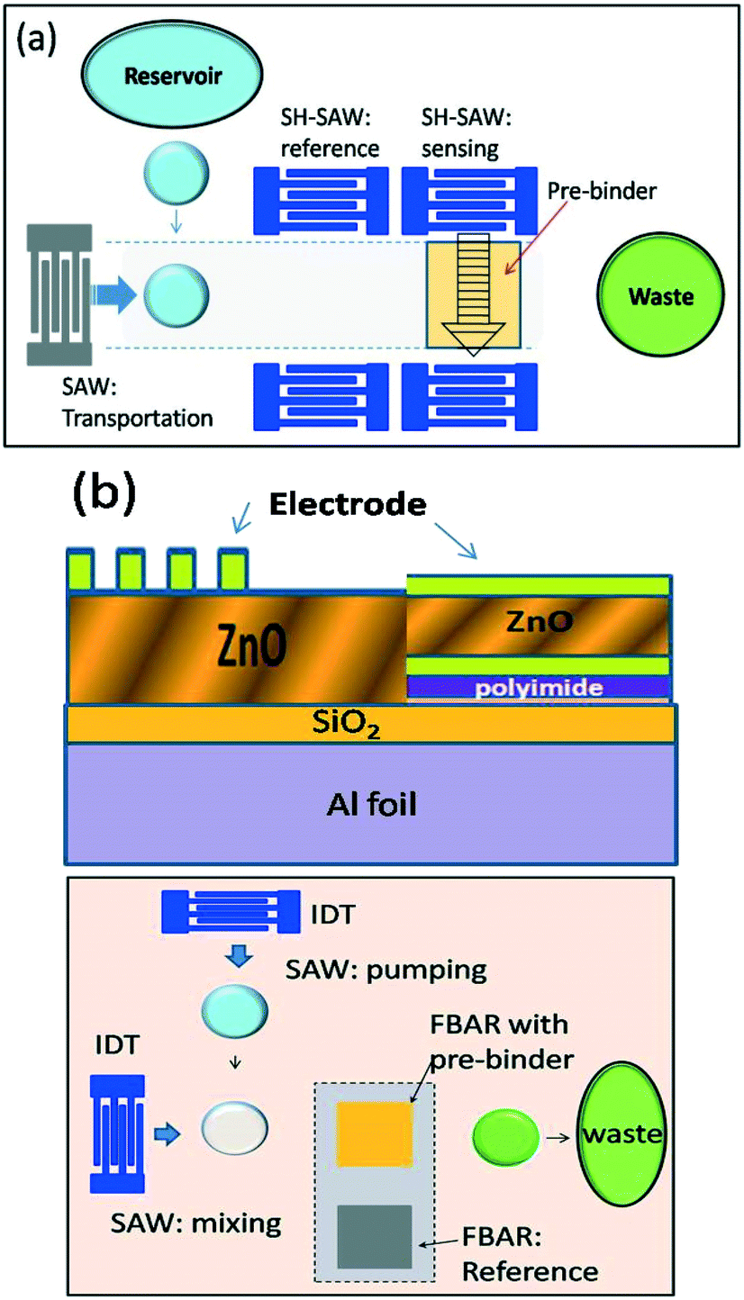 | ||
| Fig. 9 (a) Integrated liquid sensor using both Rayleigh mode SAWs and SH-SAWs on a substrate; (b) demonstration of a smart and integrated system based on SAW biosampling and liquid transportation functions and FBAR liquid sensing functions. | ||
(2) A single structure can be designed as a multimode transducer. The difference in acoustic velocities associated with different wave modes allows simultaneous optimisation of a single structure at distinct wavelengths favouring selected wave modes. In an operation scenario, this enables liquid pumping using longitudinal waves at one frequency and sensing using shear waves at another frequency.
(3) A particular configuration to simultaneously optimise the sensing and liquid manipulation functions is the integration of Rayleigh SAW and shear wave FBAR devices into a single platform. The best inclination angle should be optimised so that a single structure can be used to generate Rayleigh SAWs for liquid manipulation and shear waves in the FBAR configuration for sensitive detection.
(4) Despite its benefits in terms of multifunctionality, improved performance and high level of integration, there are technical challenges to realise this method such as the difficulty in mass production of inclined films with a uniform thickness due to the difference in the deposition rate among others. Precise control in deposition processes can provide a breakthrough point to design and develop various acoustic devices for efficient acoustofluidic manipulation and highly sensitive detection on a single platform.
(5) More studies can be focused on the mechanisms of interference of different types of wave modes and enable beam steering on a single substrate. The ability to generate different wave types on a single substrate opens the possibility of applying new techniques designed for Lamb waves, Love waves, and bulk waves into SAW devices.
Fig. 9b shows that a novel, smart and integrated system with multiple functions could be developed, based on the flexible control of the inclination angle and easy steering of the propagation of the acoustic waves on different substrates. The liquid from a reservoir will be efficiently and remotely transported to the detection area where the biobinders are located (i.e., on top of the FBAR) through conventional microchannel designs. The following SAW induced mixing will speed up the reaction and reduce the immuno-reaction time, which can minimize non-specific bonding and thus reduce faulty detection. Pairs of FBAR devices will be fabricated in order to minimize the temperature drifts and other interferences on the FBAR sensors. This can also be extended by fabricating multiple FBAR sensor arrays to provide multiple disease detection capabilities. In the MEMS process, integration is more challenging as both the SAW and FBAR device elements involve several process steps, and their process compatibility as well as single interferences will be the main focus. One inherent advantage of this design is that SAW devices and FBAR sensor arrays on the same chip can be fabricated using similar fabrication steps. A judicious selection and deposition of different immobilised bio-binders on the FBAR arrays enables the detection of different types of DNA or proteins, providing a basis for multiple disease detection. Once the reaction is complete, the SAW device can generate a wave to drive the liquid waste away. In this proposed integrated system, the droplet transportation, immobilization and detection are implemented in sequence, to minimise cross-talk and interference.
Author contributions
Y. Q. Fu: conceptualization, resources, methodology, writing-original draft, supervision, project administration, funding acquisition. H. F. Pang: investigation, visualization, data curation, writing-original draft, funding acquisition. H. Torun: visualization, data curation, validation, writing-review & editing. R. Tao: investigation, formal analysis, data curation. G. McHale: funding acquisition, validation, writing-review & editing. J. Reboud: investigation, validation. writing-review & editing. K. Tao: investigation, data curation. J. Zhou: investigation, data curation. J. Luo: investigation, funding acquisition. D. Gibson: validation, writing-review & editing. J. K. Luo: funding acquisition, writing-review & editing. P. Hu: validation, writing-review & editing.Conflicts of interest
There are no conflicts to declare.Acknowledgements
Funding support from the UK Engineering and Physical Sciences Research Council (EPSRC) under grant EP/P018998/1, Newton Mobility Grant (IE161019) through Royal Society and the National Natural Science Foundation of China, and Royal Academy of Engineering UK-Research Exchange with China and India, NSFC (51302173, 61274037, 11504291), National Key Research and Development Program of China (Grant no. 2016YFB0402705), Foundation for Distinguished Young Talents in Higher Education of Guangdong (Grant no. 2013LYM_0078), and Basic Research Program of Shenzhen (Grant no. JCYJ20140418091413493) is acknowledged. The following persons are acknowledged for their participation in the research work: Dr. Chao Zhao, Dr. Zhefeng Lei, Dr. Xiang Tao, Dr. Pep Canyelles-Pericas, Dr. Yifan Li, Mr. Andrew Bunyan, Prof. Frank Placido, Dr. Shigeng Song, Prof. William Milne, Prof. Andrew Flewitt, Dr. Mario De Miguel Ramos and Prof. Enrique Iborra.Notes and references
- R. Weigel, D. P. Morgan, J. M. Owens and A. Ballato, IEEE Trans. Microwave Theory Tech., 2002, 50, 738–749 CrossRef CAS
.
- I. Katardjiev and V. Yantchev, Vacuum, 2012, 86, 520–531 CrossRef CAS
- Y. Zhang, J. K. Luo, A. J. Flewitt, Z. Cai and X. Zhao, Biosens. Bioelectron., 2018, 116, 1–15 CrossRef CAS PubMed
- Y. Q. Fu, J. K. Luo, X. Du, A. J. Flewitt, Y. Li, A. Walton and W. I. Milne, Sens. Actuators, B, 2010, 143, 606–619 CrossRef CAS
- Y. Q. Fu, J. K. Luo, N. T. Nguyen, A. J. Walton, A. J. Flewitt, X. T. Zu, Y. Li, G. McHale, A. Matthews, E. Iborra, H. Du and W. I. Milne, Prog. Mater. Sci., 2017, 89, 31–91 CrossRef CAS
- G. Wingquist, J. Bjurstrom, L. Liljeholm, V. Yantchev and I. Katardjiev, Sens. Actuators, B, 2007, 123, 466–473 CrossRef
- X. Cao, F. Jin and J. Yang, IEEE Trans. Ultrason. Ferroelectr. Freq. Control, 2012, 59, 2522–2527 Search PubMed
- X. D. Lan, S. Y. Zhang, Y. Wan, L. Fan and X. J. Shui, Sens. Actuators, A, 2015, 230, 136–141 CrossRef CAS
- T. Yanagitani, M. Matsukawa, Y. Watanabe and T. Otani, J. Cryst. Growth, 2005, 276, 424–430 CrossRef CAS
- J. Luo, A. Quan, C. Fu and H. Li, J. Alloys Compd., 2017, 693, 558–564 CrossRef CAS
- R. Aggarwal, H. Zhou, C. Jin, J. Narayan and R. J. Narayan, J. Appl. Phys., 2010, 107, 113530 CrossRef PubMed
- F. Jose, R. Ramaseshan, S. Tripura Sundari, S. Dash, A. K. Tyagi, M. S. R. N. Kiran and U. Ramamurty, Appl. Phys. Lett., 2012, 101, 254102 CrossRef
- T. Kawamoto, T. Yanagitani, M. Matsukawa and Y. Watanabe, Jpn. J. Appl. Phys., 2010, 49, 07HD16 CrossRef
- J. Chen, H. Deng, H. Ji and Y. Tian, J. Vac. Sci. Technol., A, 2011, 29, 03A116 CrossRef
- Y. Kashiwaba, T. Abe, S. Onodera, F. Masuoka, A. Nakagawa, H. Endo, I. Niikura and Y. Kashiwaba, J. Cryst. Growth, 2007, 298, 477–480 CrossRef CAS
- T. Abe, Y. Kashiwaba, S. Onodera, F. Masuoka, A. Nakagawa, H. Endo, I. Niikura and Y. Kashiwaba, J. Cryst. Growth, 2007, 298, 457–460 CrossRef CAS
- T. Yanagitani, M. Matsukawa, Y. Watanabe and T. Otani, J. Cryst. Growth, 2005, 276, 424–430 CrossRef CAS
- R. Ro, R. Lee, Z. X. Lin, C. C. Sung, Y. F. Chiang and S. Wu, Thin Solid Films, 2013, 529, 470–474 CrossRef CAS
- J. Cui, J. Du, J. Wang and J. S. Yang, Philos. Mag. Lett., 2014, 94, 447–454 CrossRef CAS
- C. Caliendo and M. Hamidullah, J. Phys. D: Appl. Phys., 2019, 52, 153001 CrossRef
- F. Josse, F. Bender and R. W. Cernosek, Anal. Chem., 2001, 73, 5937–5944 CrossRef CAS PubMed
- G. McHale, M. K. Banerjee, M. I. Newton and V. V. Krylov, Phys. Rev. B: Condens. Matter Mater. Phys., 1999, 59, 8262–8270 CrossRef CAS
- E. Gizeli, F. Bender, A. Rasmusson, K. Saha, F. Josse and R. Cernosek, Biosens. Bioelectron., 2003, 18, 1399–1406 CrossRef CAS
- R. Friend and L. Y. Yeo, Rev. Mod. Phys., 2011, 83, 647–704 CrossRef
- L. Y. Yeo and J. R. Friend, Annu. Rev. Fluid Mech., 2014, 46, 379–406 CrossRef
- L. Y. Yeo and J. R. Friend, Biomicrofluidics, 2009, 33, 012002 CrossRef PubMed
- C. Fu, A. J. Quan, J. T. Luo, H. F. Pang, Y. J. Guo, Q. Wu, W. P. Ng, X. T. Zu and Y. Q. Fu, Appl. Phys. Lett., 2017, 110, 173501 CrossRef
- S. Brodie, Y. Q. Fu, Y. Li, M. Alghane and A. Walton, Appl. Phys. Lett., 2011, 99, 153704 CrossRef
- M. J. Fernandez, J. L. Fontecha, I. Sayago, M. Aleixandre, J. Lozano, J. Gutierrez, I. Gracia, C. Cane and M. D. Horrillo, Sens. Actuators, B, 2007, 127, 277–283 CrossRef CAS
- A. Sanz-Hervás, M. Clement, E. Iborra, L. Vergara, J. Olivares and J. Sangrador, Appl. Phys. Lett., 2006, 88, 161915 CrossRef
- M. Clement, J. Olivares, J. Capilla, J. Sangrador and E. Iborra, IEEE Trans. Ultrason. Ferroelectr. Freq. Control, 2012, 59, 128–134 Search PubMed
- A. D. Rambu, N. Iftimie and G. I. Rusu, Mater. Sci. Eng., B, 2012, 177, 157–163 CrossRef CAS
- J. G. Gardeniers, Z. M. Rittersma and G. J. Burger, J. Appl. Phys., 1998, 83, 7844–7854 CrossRef CAS
- T. Mirea, J. Olivares, M. Clement and E. Iborra, Sens. Actuators, A, 2019, 289, 87–93 CrossRef CAS
- G. Carlotti, D. Fioretto, G. Socino and L. Palmieri, Ultrason. Symp. Proc., 1990, 449–453 CAS
- H. W. Lehmann and R. Widner, J. Appl. Phys., 1973, 44, 3868–3879 CrossRef CAS
- J. S. Wang and K. M. Lakin, Appl. Phys. Lett., 1983, 42, 352–354 CrossRef CAS
- S. Maniv and A. Zangvil, J. Appl. Phys., 1978, 49, 2787–2792 CrossRef CAS
- D. Chen, J. Wang, D. Li, Y. Xu and Z. Li, Sens. Actuators, A, 2011, 165, 379–384 CrossRef CAS
- C. J. Chung, Y. C. Chen, C. C. Cheng and K. S. Kao, IEEE Trans. Ultrason. Ferroelectr. Freq. Control, 2008, 55, 857–864 Search PubMed
- C. D. Corso, A. Dickherber and W. D. Hunt, J. Appl. Phys., 2007, 101, 054514 CrossRef
- D. Chen, J. J. Wang, Y. Xu and D. Li, Sens. Actuators, B, 2012, 171–172, 1081–1086 CrossRef CAS
- J. Bjurstrom, I. Katardjiev and V. Yantchev, Appl. Phys. Lett., 2005, 86, 154103 CrossRef
- D. Chen, J. Wang, Y. Xu, D. Li, L. Zhang and W. Liu, J. Micromech. Microeng., 2013, 23, 095032 CrossRef
- I. Voiculescu and A. N. Nordin, Biosens. Bioelectron., 2012, 33, 1–9 CrossRef CAS PubMed
- W. Xu, J. Appel and J. Chae, J. Microelectromech. Syst., 2012, 21, 302–307 CAS
- R. Tao, J. Reboud, H. Torun, G. McHale, L. E. Dodd, Q. Wu, K. Tao, X. Yang, J. T. Luo, S. Todrykf and Y. Fu, Lab Chip, 2020, 20, 1002–1011 RSC
- S. H. Meng, A. C. Huang, Y. C. Chen and C. Yuan, IEEE Trans. Ultrason. Ferroelectr. Freq. Control, 2019, 66, 1014–1021 Search PubMed
- E. Milyutin, S. Gentil and P. Mutalt, J. Appl. Phys., 2008, 104, 084508 CrossRef
- E. Wajs, G. Rughoobur and A. J. Flewitt, Nanoscale, 2018, 10, 14395 RSC
- X. S. Zhou, C. Zhao, R. Z. Hou, J. Zhang, K. Kirk, D. Hutson, P. A. Hu and Y. Q. Fu, Ultrasonics, 2014, 54, 1991–1998 CrossRef CAS PubMed
- R. Hou, Y. Q. Fu, D. Hutson, C. Zhao, E. H. Gimenez and K. J. Kirk, Ultrasonics, 2016, 68, 54–60 CrossRef CAS PubMed
- G. S. K. Sabtosh and H. B. Nemade, Ultrasonics, 2015, 59, 40–44 CrossRef PubMed
- M. Clement, J. Olivares, J. Capilla, J. Sangrador and E. Iborra, IEEE Trans. Ultrason. Ferroelectr. Freq. Control, 2007, 54, 2367–2375 Search PubMed
- M. Clement, E. Iborra, J. Olivares, M. DeMiguel-Ramos, T. Mirea and J. Sangrador, Ultrasonics, 2014, 54, 1504–1508 CrossRef CAS PubMed
- E. Anderas, I. Katardjiev and V. M. Yantchev, IEEE Sens. J., 2012, 12, 2653–2654 Search PubMed
- M. DeMiguel-Ramos, B. Díaz-Durán, J. M. Escolano, M. Barba, T. Mirea, J. Olivares, M. Clement and E. Iborra, Sens. Actuators, B, 2017, 239, 1282–1288 CrossRef CAS
- A. Barranco, A. Borras, A. R. Gonzalez-Elipe and A. Palmero, Prog. Mater. Sci., 2016, 76, 59–153 CrossRef CAS
- Y. E. Lee, S. G. Kim and Y. J. Kim, J. Vac. Sci. Technol., A, 1997, 15, 1194–1199 CrossRef CAS
- K. Robbie, J. C. Sit and M. J. Brett, J. Vac. Sci. Technol., B, 1998, 16, 1115–1122 CrossRef CAS
- Y. He, J. Fu and Y. Zhao, Front. Phys., 2014, 9, 47–59 CrossRef
- K. Robbie and M. J. Brett, J. Vac. Sci. Technol., 1997, 15, 1460–1465 CrossRef CAS
- L.-C. Chen, C.-H. Tien, X. Liu and B. Xu, J. Nanomater., 2012, 2012, 409123 Search PubMed
- T. Yanagitani and M. Suzuki, Scr. Mater., 2013, 69, 724–727 CrossRef CAS
- J. K. Kwan and J. C. Sit, Sens. Actuators, B, 2013, 181, 715–719 CrossRef CAS
- D. Toledano, R. E. Galindo, M. Yuste, J. M. Albella and O. Sánchez, J. Phys. D: Appl. Phys., 2013, 46, 045306 CrossRef
- G. E. Stan, I. Pasuk, L. M. Trinca, A. C. Galca, M. Enculescu and F. Miculescu, Dig. J. Nanomater Bios., 2012, 7, 41–50 Search PubMed
- D. DeMiguel-Ramos, T. Mirea, M. Clement, J. Olivares, J. Sangrador and E. Iborra, Thin Solid Films, 2015, 590, 219–223 CrossRef
- H. Deng, J. J. Russell, R. N. Lamb, B. Jiang, Y. Li and X. Y. Zhou, Thin Solid Films, 2004, 458, 43–46 CrossRef CAS
- Y. Sato, K. Yanagisawa, N. Oka, S. Nakamura and Y. Shigesato, J. Vac. Sci. Technol., A, 2009, 27, 1166–1171 CrossRef CAS
- J. M. Nieuwenhuizen and H. B. Haanstra, Philips Tech. Rev., 1966, 27, 87–91 Search PubMed
- R. N. Tait, T. Smy and M. J. Brett, Thin Solid Films, 1993, 226, 196–201 CrossRef CAS
- S. Lichter and J. Chen, Phys. Rev. Lett., 1986, 56, 1396–1399 CrossRef PubMed
- B. Tanto, T. Eyck and T. M. Lu, J. Appl. Phys., 2010, 108, 026107 CrossRef
- H. Zhu, W. Cao, G. K. Larsen, R. Toole and Y. Zhao, J. Vac. Sci. Technol., B, 2012, 30, 030606 CrossRef
- D. Deniz, T. Karabacak and J. M. E. Harper, J. Appl. Physiol., 2008, 103, 083553 CrossRef
- L. Abelmann and C. Lodder, Thin Solid Films, 1997, 305, 1–21 CrossRef CAS
- F. Martin, M. E. Jan, S. R. Mermet and B. Belgacem, IEEE Trans. Ultrason. Ferroelectr. Freq. Control, 2006, 53, 1339–1343 Search PubMed
- T. Yanagitani and M. Kiuchi, J. Appl. Phys., 2007, 102, 044115 CrossRef
- T. Yanagitani and M. Kiuchi, Surf. Coat. Technol., 2011, 206, 816–819 CrossRef CAS
- S. Mukhtar, A. Asadov and W. Gao, Thin Solid Films, 2012, 520, 3453–3457 CrossRef CAS
- E. Iborra, M. Clement, J. Sangrador, A. Sanz-Hervás, L. Vergara and M. Aguilar, IEEE Trans. Ultrason. Ferroelectr. Freq. Control, 2004, 51, 352–358 Search PubMed
- F. Sign, P. K. Kulriya and J. C. Pivin, Solid State Commun., 2010, 150, 1751–1754 CrossRef
- M. Clement, E. Iborra, J. Sangrador, A. Sanz-Hervas, L. Vergara and M. Aguilar, J. Appl. Phys., 2003, 94, 1495 CrossRef CAS
- S. Flickyngerova, M. Netrvalova, P. Sutta, I. Novotny, V. Tvarozek, P. Gaspierik and J. Bruncko, Thin Solid Films, 2011, 520, 1233–1237 CrossRef CAS
- D. Deniz, J. M. E. Harper, J. W. Hoehn and F. Chen, J. Vac. Sci. Technol., A, 2007, 25, 1214–1218 CrossRef CAS
- H. O. Chu, S. Song, C. Li and D. Gibson, Coatings, 2017, 7, 26 CrossRef
- A. Fardeheb-Mammeri, M. B. Assouar, O. Elmazria, J. J. Fundenberger and B. Benyoucef, Semicond. Sci. Technol., 2008, 23, 095013 CrossRef
- L. Ye, S. G. Kim, Y. J. Kim and H. J. Kim, J. Vac. Sci. Technol., A, 1997, 15, 1194–1199 CrossRef
- J. C. Sit, D. Vick, K. Robbie and M. J. Brett, J. Mater. Res., 1999, 14, 1197–1199 CrossRef CAS
- D. Toledano, R. E. Galindo, M. Yeste, J. M. Albella and O. Sanchez, J. Phys. D: Appl. Phys., 2013, 46, 045306 CrossRef
- H. P. Lobl, M. Klee, R. Milsom and R. Dekker, J. Eur. Ceram. Soc., 2001, 21, 2633–2640 CrossRef CAS
- R. S. Naik, R. Reif, J. J. Lutsky and C. G. Sodini, J. Electrochem. Soc., 1999, 146, 691–696 CrossRef CAS
- H. W. Jung, H. C. Kang, D. Y. Noh and M. S. Yi, J. Appl. Phys., 2003, 94, 2957–2961 CrossRef
- D. Deniz and R. J. Lad, J. Vac. Sci. Technol., A, 2011, 29, 011020 CrossRef
- R. Triboulet and J. Perriere, Prog. Cryst. Growth Charact. Mater., 2003, 47, 65–138 CrossRef CAS
- M. Imura, K. Nakajima, M. Liao, Y. Koide and H. Amano, J. Cryst. Growth, 2010, 312, 368–372 CrossRef CAS
- G. Vogg, C. R. Miskys, J. A. Garrido, M. Hermann, M. Eickhoff and M. Stutzmann, J. Appl. Phys., 2004, 96, 895–902 CrossRef CAS
- Y. D. Jo and S. M. Koo, Appl. Surf. Sci., 2009, 255, 3480–3484 CrossRef
- X. Yuan, H. Zhou, H.-Q. Wang, X.-D. Wang, W. Geng, H. Zhan, K. Kisslinger, L. Zhang, M. Xu, Q. Y. Chen and J. Kang, Appl. Surf. Sci., 2020, 509, 144781 CrossRef CAS
- D. H. Cho, J. H. Kim, B. M. Moon, Y. D. Jo and S. M. Koo, Appl. Surf. Sci., 2009, 255, 3480–3484 CrossRef CAS
- P. Pant, J. D. Budai, R. Aggarwal, R. J. Narayan and J. Narayan, Acta Mater., 2009, 57, 4426–4431 CrossRef CAS
- Y. Kashiwaba, T. Abe, S. Onodera, F. Masuoka, A. Nakagawa, H. Endo, I. Nikura and Y. Kashiwaba, J. Cryst. Growth, 2007, 298, 477–480 CrossRef CAS
- J. Chen, H. Deng, H. Ji and Y. Tian, J. Vac. Sci. Technol., A, 2011, 29, 03A116-1-4 Search PubMed
- G. Rughoobur, M. DeMiguel-Ramos, J.-M. Escolano, E. Iborra and A. J. Flewitt, Sci. Rep., 2017, 7, 1367 CrossRef
- G. Rughoobur, M. DeMiguel-Ramos, T. C. M. Mirea, J. Olivares, B. Díaz-Durán, J. M. I. Sangrador, W. I. Milne, E. Iborra and A. J. Flewitt, Appl. Phys. Lett., 2016, 108, 034103 CrossRef
- S. Fu, Q. Li, M. Wang, C. Song, F. Zeng and F. Pan, J. Mater. Sci.: Mater. Electron., 2018, 29, 3912–3919 CrossRef CAS
- S. Bensmaine, L. Le Brizoual, O. Elmazria, J. J. Fundenberger, M. Belnahi and B. Benyoucef, Diamond Relat. Mater., 2008, 17, 1420–1423 CrossRef CAS
- S. Bensmaine, L. Le Brizoual, O. Elmazria, J. J. Fundenberger and B. Benyoucef, Phys. Status Solidi A, 2007, 204, 3091–3095 CrossRef CAS
- J. Chu, X. Peng, M. Sajjad, B. Yang and P. X. Feng, Thin Solid Films, 2012, 520, 3493–3498 CrossRef CAS
- J. M. LaForge, M. T. Taschuk and M. J. Brett, Thin Solid Films, 2011, 519, 3530–3537 CrossRef CAS
- Y. J. Park, K. M. A. Sobahan, H. J. Nam, J. J. Kim and C. K. Hwangbo, J. Korean Phys. Soc., 2010, 57, 1657–1660 CrossRef CAS
- P. Pereira-Silva, A. Costa-Barbosa, D. Costa, M. S. Rodrigues, P. Carvalho, J. Borges, F. Vaz and P. Sampaio, Thin Solid Films, 2019, 687, 137461 CrossRef CAS
- Y. F. Lai, J. H. Huang, Y. C. Chen, C. P. Liu and Y. W. Yang, J. Eur. Ceram. Soc., 2013, 33, 1809–1814 CrossRef CAS
- R. Deng, P. Muralt and D. Gall, J. Vac. Sci. Technol., A, 2012, 30, 051501 CrossRef
- J. Xiong, H. S. Gu, W. Wu, M. Z. Hu, P. F. Du and H. Xie, J. Electron. Mater., 2011, 40, 1578–1583 CrossRef CAS
- M. DeMiguel-Ramos, T. Mirea, M. Clement, J. Olivares, J. Sangrador and E. Iborra, Thin Solid Films, 2015, 590, 219–223 CrossRef CAS
- G. Rughoobur, M. DeMiguel-Ramos, T. Mirea, M. Clement, J. Olivares, B. Díaz-Durán, J. Sangrador, I. Miele, W. I. Milne, E. Iborra and A. J. Flewitt, Appl. Phys. Lett., 2016, 108, 034103 CrossRef
- J. Bjurström, G. Wingqvist and I. Katardjiev, IEEE Trans. Ultrason. Ferroelectr. Freq. Control, 2006, 53, 2095–2100 Search PubMed
- J. Munir, M. DeMiguel-Ramos, H. J. Lee, M. A. Saeed and E. Iborra, J. Microelectromech. Syst., 2017, 6, 1306–1315 Search PubMed
- M. Link, M. Schreiter, J. Weber, R. Primig, D. Pitzer and R. Gabl, IEEE Trans. Ultrason. Ferroelectr. Freq. Control, 2006, 53, 492–496 Search PubMed
- M. Link, M. Schreiter, J. Weber and R. Gabl, J. Vac. Sci. Technol., 2006, 24, 218–222 CrossRef CAS
- T. Yanagitani and M. Kiuchi, J. Appl. Phys., 2007, 102, 044115 CrossRef
- C. D. Corso, A. Dickherber and W. D. Hunt, J. Appl. Phys., 2007, 101, 054014 CrossRef
- S. Takayanagi, T. Yanagitani and M. Matsukawa, Jpn. J. Appl. Phys., 2012, 51, 07GC08 CrossRef
- H. W. Jang, H. C. Kang, D. Y. Noh and M. S. Yi, J. Appl. Phys., 2003, 94, 2957–2961 CrossRef CAS
- R. N. Tait, T. Smy and M. J. Brett, Thin Solid Films, 1993, 226, 196–201 CrossRef CAS
- C. Hu, D. Zhu, Z. He, W. Fu and Z. Qi, Appl. Surf. Sci., 2011, 257, 2801–2805 CrossRef CAS
- T. Yanagitani, N. Morisato, S. Takayanagi, M. Matsukawa and Y. Watanabe, IEEE Trans. Ultrason. Ferroelectr. Freq. Control, 2011, 58, 1062–1068 Search PubMed
- H. Zhang, Ferroelectrics, 2013, 445, 96–106 CrossRef CAS
- H. Zhang and J. A. Kosinski, IEEE Trans. Ultrason. Ferroelectr. Freq. Control, 2012, 59, 2831–2836 Search PubMed
- H. Zhang and Y. Bao, IEEE Trans. Ultrason. Ferroelectr. Freq. Control, 2014, 61, 525–534 Search PubMed
- X. Mu, P. Kropelnicki, Y. Wang, A. B. Randles, K. T. C. Chai, H. Cai and Y. D. Gu, Appl. Phys. Lett., 2014, 105, 113507 CrossRef
- J. Bjurstrom, D. Rosen, I. Katardjiev, V. M. Yanchev and I. Petrov, IEEE Trans. Ultrason. Ferroelectr. Freq. Control, 2004, 51, 1347–1353 Search PubMed
- T. Matsuo, T. Yanagitani, M. Matsukawa and Y. Watanabe, Ultrason. Symp. Proc., 2007, 1229–1232 Search PubMed
- J. M. Rouvaen, A. Menhaj-Rivenq, P. Logette, P. Goutin and F. J. Haine, J. Phys. D: Appl. Phys., 2000, 33, 1287–1297 CrossRef CAS
- C. K. Jen, J. Acoust. Soc. Am., 1988, 84, 26–29 CrossRef CAS
- L. Qin, Q. Chen, H. Cheng and Q. M. Wang, IEEE Trans. Ultrason. Ferroelectr. Freq. Control, 2010, 57, 1840–1853 Search PubMed
- K. Misu, K. Ibata, S. Wadaka, T. Chiba and M. K. Kurosawa, Trans. Inst. Electron., Inf. Commun. Eng., Sect. E, 2007, 90-A(5), 1014–1020 Search PubMed
- Q. Xiao, C. Dong, X. Ji, P. Cai and J. Chen, Symposium on Piezoelectricity, Acoustic Waves, and Device Applications, 2017, pp. 197–201.
- H. F. Pang, G. A. Zhang, Y. L. Tang, Y. Q. Fu, L. P. Wang, X. T. Zu and F. Placido, Appl. Surf. Sci., 2012, 259, 747–753 CrossRef CAS
- H. F. Pang, Y. Q. Fu, R. Hou, K. Kirk, D. Hutson, X. T. Zu and F. Placido, Ultrasonics, 2013, 53, 1264–1269 CrossRef CAS PubMed
- G. Carlotti, D. Fioretto, G. Socino, L. Palmieri, A. Petri and E. Verona, Ultrason. Symp. Proc., 1990, 449–453 CAS
- T. Yanagitani and M. Suzuki, Scr. Mater., 2013, 69, 724–727 CrossRef CAS
- G. Wingqvist, Surf. Coat. Technol., 2010, 205, 1279–1286 CrossRef CAS
- Y. Chen, P. I. Reyes, Z. Duan, G. Saraf, R. Wittstruck, Y. Lu, O. Taratula and E. Galoppini, J. Electron. Mater., 2009, 38, 1605–1611 CrossRef CAS
- E. Milyutin, S. Gentil and P. Muralt, J. Appl. Phys., 2008, 104, 084508 CrossRef
- F. Martin, E. E. Jan, S. Rey-Mermet, B. Belgacem, D. Su, M. Cantoni and P. Muralt, IEEE Trans. Ultrason. Ferroelectr. Freq. Control, 2006, 53, 1339–1343 Search PubMed
- C. J. Chung, Y. C. Chen, C. C. Cheng and K. S. Kao, IEEE Trans. Ultrason. Ferroelectr. Freq. Control, 2006, 53, 2095–2100 Search PubMed
- T. Mirea, J. Olivares, M. Clement and E. Iborra, Sens. Actuators, A, 2019, 289, 87–93 CrossRef CAS
- G. Rughoobur, H. Sugime, M. DeMiguel-Ramos, T. Mirea, S. Zheng, J. Robterson, E. Iborra and A. J. Flewitt, Sens. Actuators, B, 2018, 261, 398–407 CrossRef CAS
- M. Link, J. Webber, M. Schreiter, W. Wersing, O. Elmazria and P. Alnot, Sens. Actuators, B, 2007, 121, 372–378 CrossRef CAS
- W. Xu, X. Zhang, S. Choi and J. Chae, J. Microelectromech. Syst., 2011, 20, 213–220 CAS
- D. Chen, J. Wang, P. Wang, Q. Guo, Z. Zhang and J. Ma, J. Micromech. Microeng., 2017, 27, 045013 CrossRef
- D. Chen, S. Song, J. Ma, Z. Zhang, P. Wang, W. Liu and Q. Guo, Biosens. Bioelectron., 2017, 91, 465–471 CrossRef CAS PubMed
- D. Chen, Z. Zhang, J. Ma and W. Wang, Sensors, 2017, 17, 1015 CrossRef
- R. Hoffmann, M. Schreiter and J. Heitmann, J. Sens. Sens. Syst., 2017, 6, 87–96 CrossRef
- Y. Chen, P. Sun, C. Gao, T. Yang and Q. Huang, Mater. Express, 2020, 10, 53–61 CrossRef CAS
- J. Liu, D. Chen, P. Wang, G. Song, X. Zhang, Z. Li, Y. Wang, J. Wan and J. Yang, Talanta, 2020, 215, 120890 CrossRef CAS
- J. Weber, W. M. Albers, J. Tuppurainen, M. Link, R. Gabl, W. Wersing and M. Schreiter, Sens. Actuators, A, 2006, 128, 84–88 CrossRef CAS
- G. Wingqvist, H. Anderson, C. Lennartsson, T. Weissbach, V. Yantchev and A. Lloyd Spetz, Biosens. Bioelectron., 2009, 24, 3387–3390 CrossRef CAS
- G. Wingqvist, J. Bjurstrom, L. Liljeholm, V. Yantchev and I. Katardjiev, Sens. Actuators, B, 2007, 123, 466–473 CrossRef CAS
- G. Sharma, L. Liljeholm, J. Enlund, J. Bjurstrom, I. Katardjiev and K. Hjort, Sens. Actuators, A, 2010, 159, 111–116 CrossRef CAS
- D. Zheng, J. Xiong, P. Guo, S. F. Wang and H. S. Gu, RSC Adv., 2016, 6, 4908–4913 RSC
- Y. C. Chen, W. C. Shih, W. T. Chang, C. H. Yang, K. S. Kao and C. C. Cheng, Nanoscale Res. Lett., 2015, 10, 69 CrossRef PubMed
- Y. C. Chen, W. T. Chang, K. S. Kao, C. H. Yang and C. C. Cheng, J. Nanomater., 2013, 2013, 245095 Search PubMed
- S. Song, D. Chen, H. Wang, C. Li, W. Wang, W. Yu, Y. Wang and Q. Guo, Micromachines, 2018, 9, 501 CrossRef
- S. Song, D. Chen, H. Wang, Q. Guo and W. Yu, J. Nanosci. Nanotechnol., 2018, 18, 8099–8104 CrossRef CAS
- X. Zhu and E. S. Kim, Sens. Actuators, A, 1998, 66, 355–360 CrossRef CAS
- H. Yu, Q. Zu, J. W. Kwon, D. Huang and E. S. Kim, J. Microelectromech. Syst., 2007, 16, 445–453 CAS
- J. W. Kwon, H. Yu, Q. Zou and E. S. Kim, J. Micromech. Microeng., 2006, 16, 2697–2704 CrossRef CAS
- C. Y. Lee, W. Pang, H. Yu and E. S. Kim, Appl. Phys. Lett., 2008, 93, 034104 CrossRef
- A. Fardeheb-Nammeri, M. B. Assonar, O. Elmazria, J. J. Fundenberger and B. Benyoucef, Semicond. Sci. Technol., 2008, 23, 095013 CrossRef
- A. Kochhar, Y. Yamamoto, A. Teshigahara, K. Y. Hashimoto, S. Tanake and M. Esashi, IEEE Trans. Ultrason. Ferroelectr. Freq. Control, 2016, 63, 953–960 Search PubMed
- Y. Li, R. Y. Fu, D. Winters, B. W. Flynn, B. Parkes, D. S. Brodie, Y. Liu, J. Terry, L. I. Haworth, A. S. Bunting, J. T. M. Stevenson, S. Smith, C. L. Mackay, P. R. R. Langridge-Smith, A. A. Stokes and A. J. Walton, IEEE Trans. Semicond. Manuf., 2012, 25, 323–330 Search PubMed
- P. Sheng and W. Wen, Annu. Rev. Fluid Mech., 2012, 44, 143–174 CrossRef
- R. D. Sochol, E. Sweet, C. C. Glick, S.-Y. Wu, C. Yang, M. Restaino and L. Lin, Microelectron. Eng., 2018, 189, 52–68 CrossRef CAS
| This journal is © The Royal Society of Chemistry 2021 |