DOI:
10.1039/D0LC00751J
(Paper)
Lab Chip, 2020,
20, 4106-4117
High-throughput roll-to-roll production of polymer biochips for multiplexed DNA detection in point-of-care diagnostics†
Received
24th July 2020
, Accepted 6th October 2020
First published on 22nd October 2020
Abstract
Roll-to-roll UV nanoimprint lithography has superior advantages for high-throughput manufacturing of micro- or nano-structures on flexible polymer foils with various geometries and configurations. Our pilot line provides large-scale structure imprinting for cost-effective polymer biochips (4500 biochips/hour), enabling rapid and multiplexed detections. A complete high-volume process chain of the technology for producing structures like μ-sized, triangular optical out-couplers or capillary channels (width: from 1 μm to 2 mm, height: from 200 nm up to 100 μm) to obtain biochips (width: 25 mm, length: 75 mm, height: 100 μm to 1.5 mm) was described. The imprinting process was performed with custom-developed resins on polymer foils with resin thicknesses ranging between 125–190 μm. The produced chips were tested in a commercial point-of-care diagnostic system for multiplexed DNA analysis of methicillin resistant Staphylococcus aureus (e.g., mecA, mecC gene detections). Specific target DNA capturing was based on hybridisation between surface bound DNA probes and biotinylated targets from the sample. The immobilised biotinylated targets subsequently bind streptavidin–horseradish peroxidase conjugates, which in turn generate light upon incubation with a chemiluminescent substrate. To enhance the light out-coupling thus to improve the system performance, optical structures were integrated into the design. The limits-of-detection of mecA (25 bp) for chips with and without structures were calculated as 0.06 and 0.07 μM, respectively. Further, foil-based chips with fluidic channels were DNA functionalised in our roll-to-roll micro-array spotter following the imprinting. This straightforward approach of sequential imprinting and multiplexed DNA functionalisation on a single foil was also realised for the first time. The corresponding foil-based chips were able to detect mecA gene DNA sequences down to a 0.25 μM concentration.
1. Introduction
Microfluidic biochips enable miniaturised and automated standard, wet-lab processes, to be performed both for clinical and research applications. These biochips typically comprise fluidic structures for liquid handling, chambers for (bio-) chemical reactions as well as detection regions for signal readouts. These lab-on-a-chip (LoC) products are used in diverse fields, such as, DNA1,2 or protein arraying,3 genome sequencing,4,5 protein6,7 or exosome profiling,8 and studies of cell activity9 or cell-to-cell interaction.10 With the increasing maturation of the technology, biochips hold their place in in vitro diagnostic (IVD) applications. Automation and multiplexing of biochips provide significant cost reduction and increased test efficiencies with shortened testing times. For instance, microfluidic LoC platforms such as infection detection systems,11 provide convenient and rapid multiplexed testing of pathogens of interest. The envisioned widespread use of such tests (e.g., for severe hospital infections), requires finding cost-effective solutions for large-scale production technologies of these biochips. Currently, most of the microstructures in biochips used for IVD applications, are produced via injection moulding.12 Although the injection-moulding technique provides rapid and reproducible productions of the microstructures, only individual chips are produced via this sequential process. Moreover, chip handling is quite complex in each post-processing step. Oppositely, large area roll-to-roll (R2R) imprinting enables parallel and high-throughput generation of micro- or even nano-structures in various designs.13,14 Since, the production is performed on a flexible polymer foil, post-processing (e.g., bio-functionalisation, chip lamination) is also possible via the R2R manufacturing approach. The post-processing flexibility in R2R processes enables facile production of chips on large area polymer substrates. The imprinting applied to flexible polymer foils with a usual foil thickness of ∼100 μm, provides relatively low material costs and tailored characteristics to the disposable biochips used in LoC applications.15 Basically, R2R imprinting processes can be divided into three categories, based on production technologies: extrusion coating,16 ultraviolet nanoimprint lithography (UV-NIL)17 and thermal NIL18 or hot embossing (HE).19 The production of structures down to nanometre-range feature size is achieved via UV-NIL technology, which was first introduced by J. Haisma and co-workers.20 The technology was then implemented as R2R, for the first time by S. H. Ahn and L. J. Guo.21 The R2R UV-NIL technology can be applied to flexible polymers (e.g., metal foil, paper, flexible glass, PS, PET, PEEK, PP and PEN§)22–26 In our R2R UV-NIL process, structures are transferred from a large polymer, nickel or steel stamp, so-called “shim”, to an uncured, acrylate-based photoresin, which is initially rotogravure printed onto a polymer foil (shown in Fig. 1).13,27–30 While in contact with the shim, UV light cures the photoresin and solid structures with high resolutions are efficiently obtained on the foil. Our imprinting technology done at room temperature and low pressure under ambient air conditions, enables producing micro- or nano-structures in various length scales13 and geometries like V-grooved or rectangular channels. Therefore, obtaining an aspect ratio up to 5![[thin space (1/6-em)]](https://www.rsc.org/images/entities/char_2009.gif) :1 (height:line) is possible. Our R2R technology has high potential for upscaling of production processes and reduction of process costs per piece of LoC devices. Within this context, R2R imprinting techniques offer superior industrial solutions for production of micro- or nano-structures in terms of reduced process costs and improved manufacturing throughput.31
:1 (height:line) is possible. Our R2R technology has high potential for upscaling of production processes and reduction of process costs per piece of LoC devices. Within this context, R2R imprinting techniques offer superior industrial solutions for production of micro- or nano-structures in terms of reduced process costs and improved manufacturing throughput.31
 |
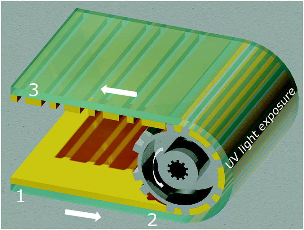
| | Fig. 1 The illustration of our roll-to-roll (R2R) UV nanoimprint technology. (1) A transparent, thermoplastic foil (green) is reverse rotogravure printed13 with a liquid, custom-made photoresin (yellow) prior to the imprinting. (2) A hard stamp (grey) wrapped over the web, continuously transfers micro- or nano-structures into the uncured photoresin. Simultaneously, the photoresin is cured by a LED UV light source from the backside of the foil, at room temperature. (3) As the stamp detaches from the cured photoresin, robust structure patterning is obtained. The arrows indicate the movement directions of the polymer foil, as well as the web. | |
In this study, multiplexed DNA biosensing applications of our high-throughput R2R UV-NIL produced polymer based fluidic chips with different features were demonstrated (e.g., light enhancing structures or micro-spotted DNA probes). The produced disposable R2R biochips were used for detecting DNA sequences representing methicillin-resistant Staphylococcus aureus (MRSA) in a commercially available IVD as a model system. The detection of the specific genes in this system is based on a chemiluminescence reaction. MRSA can be considered as the major source of serious healthcare-associated infections worldwide.32 Due to chromosomal mutations occurring in the genomic material of MRSA, it becomes resistant to penicillin and its derivatives like methicillin, which is a synthetic form of penicillin.33 In MRSA genome, genes mecA34 and mecC, which is also a mecA homologue,35–37 are known for encoding low-affinity penicillin-binding proteins; thus, providing an extreme resistance to beta-lactam antibiotics.38,39 The rapid detection of its trace in low levels within the human blood plays a vital role in preventing a clinical spread and providing an early treatment for the infected patient. Therefore, R2R UV-NIL biochips with light out-coupling structures were optimised to lower the limit-of-detection (LoD) of the mecA gene DNA sequences. Firstly, R2R imprinting was used to enhance the performance of a commercially available injection-moulded chip, tested in an MRSA detection system. Secondly, the R2R imprinting was demonstrated as a full replacement for the injection-moulded chip. At this step, the fluidic patterns were replicated by R2R imprinting. In order to move the concept of the multiplexed DNA detection via biochips a step further, a R2R micro-array spotting pilot line for foil-based microfluidic chips was implemented for the first time. Using this equipment, DNA probes were spotted into the imprinted fluidic structures and complete foil-based chips were prepared and tested inside the IVD system.
2. Materials
For direct write laser photolithography purposes, silicon wafers (diameter: 4′′) were purchased from Si-Mat-Silicon Materials e. K. (Germany). For the primary optic master production, a low contrast and positive-tone AZ® 9260 photoresist was purchased from MicroChemicals GmbH (Germany). For the replication of a secondary master, polydimethylsiloxane (PDMS) SYLGARD® 184 silicone elastomer kit (a two compound system) was purchased from Baltres Handelsges.m.b.H. (Austria). Custom-made, acrylate-based photoresins were used during the R2R UV-NIL process: mr-NIL500SF-XP (dynamic water contact angle: 110 ± 3°, refractive index: 1.59) and hydrophilic mr-BioNIL100SF-XP (dynamic water contact angle: 49 ± 5°, refractive index: 1.48, both developed by micro resist technology GmbH, Germany). For mastering of the fluidic structures, a dry film photoresist Ordyl® SY-300 (nominal thickness: 90 μm, ElgaEurope S.r.l., Italy) was utilised during the photolithography. For R2R UV-NIL processes, a PS foil with 190 μm thickness (4titude® Ltd., UK) and a PET foil with 125 μm thickness (Melinex® ST505, DuPont Teijin Films, USA) were used. For DNA functionalisation, a UV curable DNA linker, sciPOLY3D DNA solution (sciPOLY3D SOL2D1 and sciPOLY3D LIQUID, SCIENION AG, Germany) was utilised. The sciPOLY3D DNA solution is composed of a hydrophilic matrix, a water solubility enhancer and a photo-reactive group.40Staphylococcus epidermidis PQ101 (SE), negative control PQ40 (NC), methicillin-resistant PQ104 (mecA) and PQ105 (mecC), Staphylococcus aureus PQ102 (SA), polymerase-chain-reaction (PCR) control PQ103 (PC) and hybridisation control (HC) single stranded DNA (ss-DNA) probes and their fully DNA counterparts were utilized in this study. SE, NC, mecA, mecC, SA and PC oligos were 25 bp-long while HC oligos were 105 bp-long. All oligos were synthesised with high purity and target ss-DNAs were biotinylated by Microsynth Austria GmbH (Austria). To make ss-DNA stripes visible on the chip foil, brilliant blue G (CAS number: 6104-58-1, Sigma-Aldrich, Germany) was used in capillary DNA printing. Custom-made solutions: GENSPEED® C (containing 80% v/v H2O and 20% v/v of 12.5 nM HC targets), 1X R2R solution (containing 81% v/v GENSPEED® C, 1% v/v target oligos, 18% v/v H2O), GENSPEED® D (i.e., an enzyme), GENSPEED® E (a stringent salt solution to remove non-specifically bound ss-DNAs) and GENSPEED F, a chemiluminescent (CL) solution, were provided from GENSPEED Biotech GmbH (Austria). The biotinylated targets (b-DNAs) were composed of all targets (except for HC targets) with a concentration of 1 pmol μL−1 of each. Additionally, molecular biology (MB) grade H2O from Carl Roth GmbH + Co. KG (Germany) was used throughout the study. In all biochip testing, GENSPEED® R1 MRSA testings device (GENSPEED Biotech GmbH, Austria) was utilised.
3. Methods
3.1. GENSPEED MRSA sensing
The GENSPEED® R1 device is the first generation of GENSPEED® IVD medical devices used for early detection of hospital-acquired infections due to specific pathogens, such as MRSA,41Clostridium difficile,42 and also for the detection of bacterial vancomycin resistant43 and carbapenemase genes.44 For that reason, certain b-DNAs are used in the testing procedure. In the intended use of a commercial R1 device, DNA amplicons produced from patients samples are used as targets. After sampling using nasal, throat or inguinal swab, the DNA is released from the cells using a combined chemical and heating lysis. Then the sample is amplified by polymerase chain reaction and simultaneously labelled with biotin. The amplicon is then mixed with a proprietary hybridization solution, denatured at 95 °C and pipetted into the GENSPEED MRSA test chip to allow binding of the labelled DNA to the complementary probes in the GENSPEED MRSA test chip. To mimic that process and at the same time have a reproducible test sample, we used synthetic biontinylated, single-stranded DNAs (i.e., b-DNAs) as targets. These b-DNAs were synthesized by Microsynth (Austria). The R1 system is an opto-electronic detection platform and it consists of a disposable biochip and the device with a tray (Fig. S1 in ESI†).
The chip is inserted into the device tray, under which a photodiode array is located. The ss-DNA targets are detected via a CL based detection method, in ∼9 min except for the pre-treatment of the targets (i.e., sample amplification and biotinylation).45 Based on this technique, b-DNAs are captured by the surface bound probes. Such a detection is achieved by obtaining a recognition based on “solid phase DNA hybridisation” between probes and their full-length counterparts (i.e., targets).46 Following GENSPEED® solution C pipetting into the inlet, GENSPEED® solution D is also manually introduced to the reaction channel to detect b-DNAs, which are bound to the surface probes. Following the enzyme introduction throughout the fluidic channel, GENSPEED® solution E is sent to remove unbound residuals. Then, GENSPEED® solution F is sent in order to initiate a CL reaction over the captured targets. Then, the CL signal is transduced to the photodiode array located under the chip with 32 photodiodes (i.e., pixels). The ss-DNA probes deposited at the test chip are given with their corresponding pixel numbers in the photodiode array (Fig. S2 and Table S1 in ESI†). For LoD determination, 1X R2R solution in GENSPEED® solution C as well as its serial dilutions with GENSPEED® solution C (1:2, 1:4, 1:8, 1:16 and 1:32 v/v) were utilised for each measurement. GENSPEED® solution C prevents secondary DNA structure formation in buffer to yield higher DNA hybridization efficiency at room temperature. During our studies, all blank measurements were performed using GENSPEED® solution C containing HC (i.e., hybridisation control) targets only. In all experiments, a total sample volume of 20 μL was used. The measurement protocols for all testings were provided in Table S2 (ESI†). The introduction of GENSPEED® solutions D, E and F into the chip inlet was performed manually and consecutively, according to manufacturer's protocol. In all testings, GENSPEED® R1 MRSA testing device was operated at 25 °C.
3.2. Description of the biochips
For testing, three sorts of biochips were used. All chips were produced by combining two different chip parts with different techniques (see Table 1). First GENSPEED® biochip design (length: 75 mm, width: 25 mm, height: 1.5 mm) was composed of an injection-moulded upper part (Chip1, Fig. 2A and S3 in ESI†) and a flexible and PS foil with ss-DNAs probes possessing different sequences (Fig. 2B, blue stripes). The top part of the chip was an injection-moulded PS chip part with (1) an inlet port, (2) a capillary-force driven fluidic or reaction channel (length: 37 mm, width: 2 mm, height: 100 μm) and (3) an outlet or waste reservoir. To decrease the contact angle and enable appropriate flow within the channel, the top part is coated via a proprietary plasma polymerisation process prior to chip bonding. The target solution, which was placed manually to the inlet port, moves through the reaction channel towards the waste reservoir by capillary forces. The capillary movement towards the waste enables flushing of the channel prior to the introduction of different reagents, during the analysis. In order to perform a multiplexed DNA testing on a single chip, the bottom foil of the chip has stripes with different ss-DNA probes tethered (i.e., SE, NC, mecA, mecC, SA, PC and HC). The probe ss-DNAs were printed onto the PS foils using a capillary printer (BioDot™ Inc., USA). For printing, the lyophilised sciPOLY3D product was reconstituted in molecular biology grade H2O by vortexing at room temperature, to a final concentration of 5 mg ml−1. A printing buffer consisting of 50% v/v sciPOLYSol2, 20% v/v sciPOLY3D (5 mg ml−1), 28% v/v brilliant blue G solution (0.3% v/v in H2O) and 2% v/v GENSPEED® standard printing solution, was utilised to attach ss-DNA probes. Prior to use, the printing buffer was filtered with a 100 μm pore-sized EASYstrainer™ cell sieve (Greiner Bio-One GmbH, Austria). Probe ss-DNAs (2 μM in printing buffer) were capillary printed as 7 separate stripes: SE, NC, mecA, mecC, SA, PCR and HC probes (0.30 μl cm−1 dispensing volume, 12 cycles for each). Each stripe (length: 2.5 cm, width: 0.05 cm) was printed using 2% v/v probe ss-DNA in the printing buffer. After the ss-DNA printing process, the foils were incubated at 50 °C for 30 min, and then dried for 15 min at room temperature. The fixation of the stripes was performed by curing of the DNA linker for 2 min using a UV lamp (Analytic Jena AG, Type UVC 500, Germany) with a light dose of 1.25 J cm−2 at a wavelength of 254 nm. Then, the foils were cut into 2.5 cm × 7.5 cm dimensions using a plot cutter. Finally, the foils were laminated to the GENSPEED® standard top parts using an ultrasonic welding machine (Herrman™ Ultrasonics, USA).
Table 1 Types of the biochips produced throughout this study
| Types |
Description |
| Chip1 |
Fluidic chips without optical structures, with injection-moulded top covers and capillary printed probe ss-DNAs. The chip is ultrasonically bonded. |
| Chip2 |
Fluidic chips with optical structures, injection-moulded top covers and capillary printed probe ss-DNAs. The chip is ultrasonically bonded. |
| Chip3 |
Completely foil-based fluidic chips with probe ss-DNA micro-spots. The chip is bonded via a glue printing technique. |
 |
| | Fig. 2 The illustration of the biochip with injection-moulded top cover (i.e., Chip1). (A) The rigid PS top part with the fluidic channel. (1), (2) and (3) refer to an inlet, a reaction channel and an outlet, respectively. (B) A flexible and plain PS foil with the capillary printed probe ss-DNAs (shown as blue stripes) allowing DNA–DNA hybridizations. The parts (A) and (B) are combined with an ultrasonic bonding technique. The total biochip height is 1.5 mm. | |
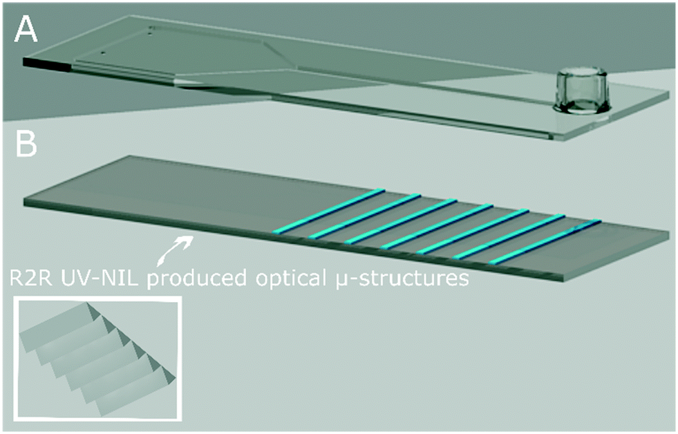
For the second chip type (i.e., Chip2), the identical injection moulded chip design was equipped with modified bottom foils. For this purpose, light out-coupling optical microstructures in triangular geometry (described in Fig. 3A and B) were R2R UV-NIL imprinted at the bottom chip part to the side facing the photodiode array (i.e., the second chip type). The detailed photographs of the chip with the optical structures were provided in Fig. S4 (in ESI†). The triangular microstructure geometry was found to be the most efficient one, as a result of the performed simulations, which employ simplified models using classical ray-tracing method (Breault Research Organization, USA). Via the optical microstructures, it was aimed to enhance the light out-coupling efficiency of generated chemiluminescent signal inside the reaction channel reaching the photodiodes inside the device. The bonding of the two biochips parts were again achieved via the ultrasonic welding machine.
 |
| | Fig. 3 The illustration of the biochip with R2R UV-NIL produced light out-coupling microstructures (i.e., Chip2). (A) The injection-moulded upper part, owning the same design in Fig. 2A. (B) The bottom chip part, sharing the same design in Fig. 2B. The inset shows the side with the R2R UV-NIL imprinted triangular optical microstructures, enhancing the light out-coupling from the polymer foil towards the detector of GENSPEED R1 device. The microstructures are imprinted at the foil side facing the photodiode array in the device. The parts (A) and (B) are combined with the ultrasonic bonding technique. Inset shows the micro-structures as a closer-look. The total biochip height is 1.5 mm. | |
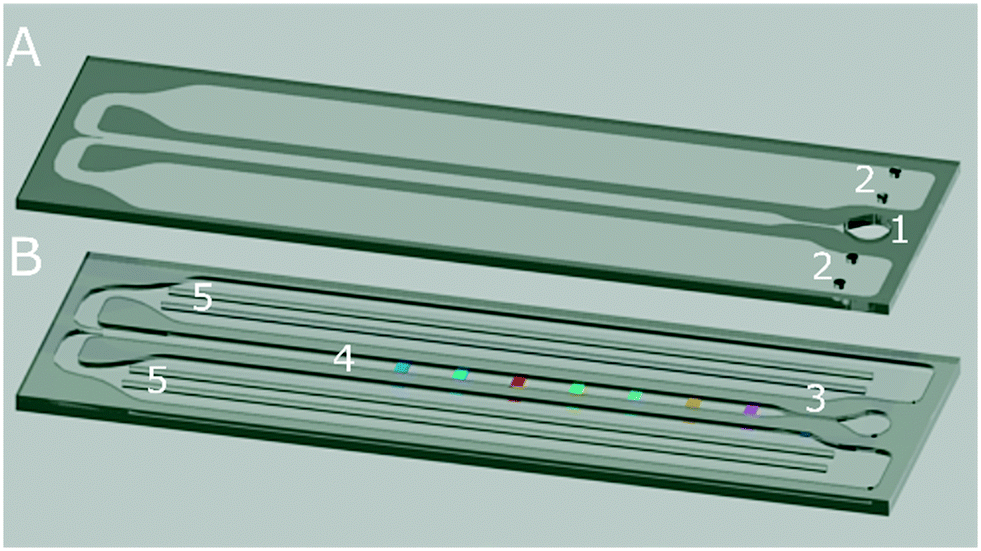
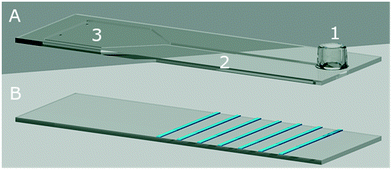
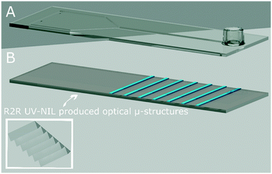
The third type of the tested chips (i.e., Chip3) were fully foil-based R2R chips (length: 75 mm, width: 25 mm, height: 100 μm) consisting of two main parts (shown in Fig. 4A and B). The lower part of the chip (Fig. 4B) was a R2R UV-NIL structured PET foil with fluidic channels (channel length: 60 mm, width: 2.7 mm, height: 70 μm). This R2R UV-NIL structured fluidic parts were subjected to R2R micro-array spotting unit for bio-probe tethering (undermentioned in detail in section 3.3.2.). After the bio-functionalisation, sheets containing several copies of the chip part were cut using a CO2 laser cutter (60 W, Speedy 300 Flexx, Trotec, Austria). The bonding of Chip3 was achieved via a glue printing technique. The screen printing of an acrylate based, pressure sensitive adhesive, KIWOPRINT D158 (Kissel + Wolf GmbH, Germany) was performed on PS foils (i.e., upper parts) for chip bonding. Prior to the screen printing, the bare PS foils were laser marked with four identical fiducials to align the adhesive layer to the chip part during the printing process (indicated in Fig. 5 by arrows). Then, the inlet (diameter: 4 mm) and the air ventilation sections (diameter: 1 mm) were drilled using the CO2 laser. The printing screen was designed as the inverse of the fluidic structures, so that only the outer part of the imprinted patterns were covered with the glue (Fig. 5). The glue contains a solvent, which was evaporated after printing, providing an adhesive layer. Following the glue printing, the upper parts were separated into sheets matching the format of the fluidic parts via the laser cutting process. The lamination of these flexible chip parts was performed in a rolling mill machine (at 50 °C, 1.3 m min−1 rolling vitesse, 2 passes, BlackHole Lab, France) under dust-free conditions.
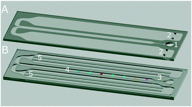 |
| | Fig. 4 The illustration of our foil-based, R2R UV-NIL produced DNA biochip (i.e., Chip3). (A) The glue printed, upper PS chip part. The glue is printed at the side facing the structured bottom part. The inlet (1) and the air ventilation holes (2) are drilled with a CO2 laser, prior to the chip lamination process. (B) The R2R UV-NIL structured PET bottom part with capillary-force driven channels. (3), (4) and (5) refer to the retarding channel (length: 5 mm, width: 200 μm, height: 70 μm), the reaction channel (length: 37 mm, width: 2.7 mm, height: 70 μm) with different probe ss-DNA micro-spots and the waste channels on both sides, respectively. Inside the reaction channel, multiplexed probe DNAs allowing DNA–DNA hybridizations (shown with different colors) are R2R micro-spotted. The two chip parts are combined using a rolling mill machine. The total biochip height is 100 μm. | |
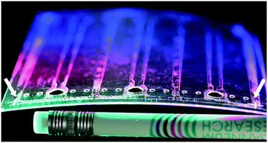 |
| | Fig. 5 The glue printed PS upper parts for foil-based biochips. The adhesive printing is made to comply with the outer part of the fluidic channels and the space between them. For a precise printing, the plain PS foil is laser marked first with plus-shaped fiducials (indicated by arrows). Following the printing, the inlets (diameter: 4 mm) and the air ventilation holes (diameter: 1 mm) are drilled under a CO2 laser (60 W). The parts are further laser cut and separated from each other prior to the chip lamination process. | |
3.3. R2R UV-NIL production
3.3.1. Imprinting of the optical microstructures.
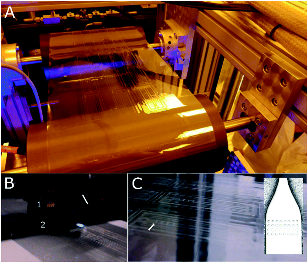
For the primary master fabrication via custom-made, maskless greyscale UV-laser lithography (MALA) operating at 375 nm wavelength, a silicon wafer was spin-coated with AZ® 9260 (thickness: 40 μm) photoresist. A focused UV-laser beam was scanned with controlled light intensity over the sample. Following the wet development of the patterned photoresist, the continuous-relief optical microstructures were obtained. A soft-stamp (i.e., the, secondary master) was made by mixing the SYLGARD® 184 silicone elastomer kit with a ratio of 10:1 w/w, respectively. This mixture was casted onto the polymer master and degassed in a vacuum chamber for 2 hours. The curing of the mixture was performed at 25 °C for 72 h. Then, the PDMS mould was detached from the poylmer master. The soft mould was used for fabricating an inverse structure based on polyurethane acrylate on a quartz template for step-and-repeat purposes. In order to produce large imprinting shims, a PET substrate was sequentially patterned using a custom-made imprinting resin (i.e., NILcure JR82) with a customised EVG®770 automated NIL stepper (EV Group, Austria). The NIL stepper was able to position pattern fields accurately onto the substrate with 5 μm positioning accuracy over a 300 × 300 mm area. After the liquid resin filled the stamp patterns, the resin was UV-cured through the transparent stamp. The shim was covered with a Cr (thickness: 3 nm)/Al (thickness: 50 nm) layer and a fluorine-based anti-adhesive13 prior to its use as the imprinting roller. To perform the R2R UV-NIL process, the polymer shim was wrapped over a steel roller in the R2R UV-NIL pilot line (Fig. 6A). The life-time of this shim allows imprinting of several hundred meters of the polymer foil corresponding to 7500 chips per 100 m. Following unwinding of the carrier PS foil (width: 250 mm) from the roll, the reverse rotogravure printing of mr-NIL500SF-XP photoresin, was performed using a Basecoater BC44 (5 m min−1, Coatema Coating Machinery GmbH, Germany), shown in Fig. 6B. As the structures were imprinted onto the foil, the backside of the transparent foil was exposed to UV-light, with an irradiance of 2.2 W cm−2 from a LED UV lamp, to cure the imprinted structures. Solely, the R2R UV-NIL unit of the pilot line is illustrated schematically in Fig. 6C, where the photoresin with the imprinted structures is displayed in yellow colour. The R2R UV-NIL process was performed at room temperature with a web tension of ∼100 N. During the imprinting, a pressure of 1 N per line was applied by the counter roller to the main roller to ease the process. Finally, the roll was rewinded to collect the imprinted section of the polymeric foil (Fig. 6B). In addition, the photograph of the imprinted optical microstructures, on the PS foil, is provided in Fig. 6D.
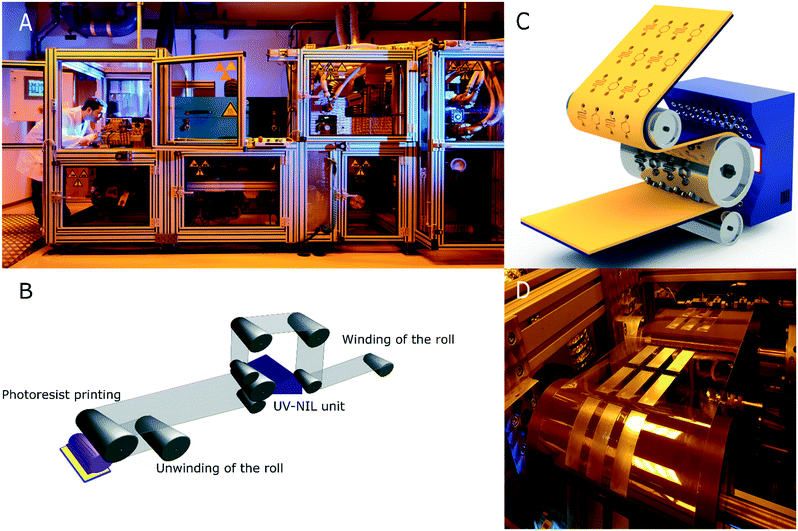 |
| | Fig. 6 Production of the optical microstructures via our R2R UV-NIL technology for enhancing the light out-coupling in LoC based IVDs. (A) The photograph of our R2R UV-NIL pilot line for industrial scaling. (B) A drawing demonstrating the R2R UV-NIL process line, which starts with unwinding of the roll, photoresin coating, UV-NIL imprinting and winding of the roll, serially. (C) The schematic illustration of the UV-NIL unit in the R2R pilot line. The optical microstructures are imprinted on the photoresin coated (yellow) transparent PS foil (190 μm thickness), using a steel shim (grey) mounted over the imprint roller (web width: 250 mm), which moves at a speed¶ of 5 m min−1. The backside of the transparent foil is exposed to UV light radiating from a 395 nm LED UV light source (2.2 W cm−2), which is located inside a UV screen (white). (D) A photograph of the imprinted optical microstructures (chip format with length: 7.5 cm length, width: 2.5 cm) on a flexible PS foil coated with the structured acrylate-based photoresin. | |
3.3.2. Imprinting and bio-functionalisation of the fluidic channels.
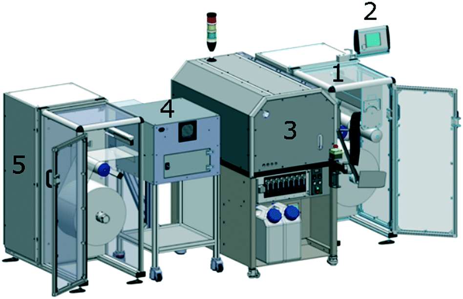
In order to produce a shim for R2R UV-NIL imprinted fluidic channels, the structures were initially mastered by photolithography in Ordyl® SY-300. The master structure was composed of three identical fluidic chip parts, placed at a certain distance from each other (i.e., the primary master). INMOLD A/S (Denmark) produced a polymer shim of the fluidic channels by replicating the master in a custom-made photoresin (OrmoComp® developed by micro resist technology GmbH, Germany), which was used for imprinting. Prior to the R2R UV-NIL process, the polymer shim was metallized with chromium/aluminium and further, functionalised with the fluorinated anti-adhesive. The film thicknesses of chromium and aluminium were 4 nm and 50 nm, respectively. The shim design contained a fiducial (see Fig. S5 in ESI†), located at top of each inlet, to obtain an accurate position for the ss-DNA bio-functionalisation. Finally, imprinting of the fluidic channels was performed on a PET foil with rotogravure-coated hydrophillic mr-BioNIL100SF-XP (imprinting speed: 1 m min−1). Via our technology, 4500 biochips/hour can be fabricated. The UV curing parameters of this R2R UV-NIL process was kept the same, as provided under section 3.3.1. The complete R2R UV-NIL structured polymer foil was then inserted to the unwinding section of our R2R micro-array spotting line (Fig. 7-(1)), which was located at a separate working area (Fig. 7 and S6 and Video S1 in ESI†). Fig. 8A shows the imprinted fluidic channels, prior to the R2R micro-spotting process. The bottom chip parts on the unrolled foil enters part-by-part into the medium-scale micro-spotting section (Fig. 8B), with a web speed of 5 m min−1 in a stop-and-go process. This automated pilot line owns the medium scale micro-spotter (sciFLEXARRAYER S12®, SCIENION AG, Germany) for batch productions with a spotting area of 300 mm and 375 mm in width and length, respectively. For each section of the PET foil entering to the spotting line for a bio-functionalisation, a chip configuration of 3 columns and 3 rows (i.e., 9 chips/run) was spotted, based on our imprinting design. The imprinted fiducials were automatically recognised by the software via the head camera located nearby the nozzle head (see Fig. 8B) ensuring an accurate micro-array spotting into each reaction channel (see Fig. 4B-(4)). Into each reaction channel, multiplexed ss-DNA spotting was performed using a piezo dispense capillary (PDC) glass nozzle (Fig. 8B-1 and 2), with an inner coating suitable for enhanced DNA spotting applications (PDC90, Type1 coated, SCIENION AG, Germany). Seven different GENSPEED MRSA probes were micro-spotted for that purpose. A DNA buffer consisting of 50% v/v sciPOLYSol2, 20% v/v sciPOLY3D (5 mg ml−1), 12% v/v ss-DNA solution (100 μM in MB grade H2O) and 18% v/v H2O, was utilised to tether ss-DNA probes onto the surface. Prior to the spotting process, no pre-surface functionalisation was applied. The DNA spotting was performed at 25 °C and 38 ± 2% relative humidity, supplied by a humidifier in the micro-spotting system. The ss-DNAs were micro-spotted onto the locations with high accuracy (<1 μm), corresponding to the same photodiode pixel positions of the injection-moulded chips (see Table S1†), to which ss-DNAs were capillary printed (Fig. 8C). Each corresponding pixel area with tethered ss-DNAs was 0.9 mm in width and 3.7 mm in length allowing 4 rows and 18 columns of ss-DNA spots, 2 drops/spot, 400 pL per drop with 220 μm pitch distance (Fig. 8C, inset). Following the micro-spotting process, each ss-DNA spotted part of the foil was moved into the UV curing section located behind the micro-spotter, at which the spots got cured under a UV irradiance of 27.5 mW cm−2 (at 254 nm) for 3 min (Fig. 7-(4)). The DNA bio-functionalisation process was completed by winding the roll again inside a re-winder (Fig. 7-(5)). The foil chips were laminated via the procedure described under section 3.2 (see Fig. S7† and capillary-flow shown in Video S2, ESI†).
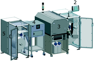 |
| | Fig. 7 High-throughput R2R micro-array spotting pilot line for chip biofunctionalisation. R2R UV-NIL structured polymer foil is wrapped over a web inside the unwinder (1). The stop-and-go movement of the foil is monitored with a manual screen (2). The medium-scale micro-array spotter enabling multiplexed spotting and the control panel nearby (3). The micro-spotter is equipped with a humidifier and a chiller. The micro-spotter has access to a UV lamp (width: 300 mm, length: 300 mm) enabling curing of the DNA micro-spotted sections of foil. The UV unit is equipped with 12 tube UV lamps (7.3 W, emitting at 254 nm) and combined with a cooling unit (4). The complete line is fully automated and UV radiation is activated on command via the custom-developed software, controls the movement of a mechanical shutter. Following curing, the foil is wrapped, inside re-winding unit (5). | |
 |
| | Fig. 8 High-throughput R2R based ss-DNA micro-spotting. (A) R2R UV-NIL imprinted bottom parts located on a PET foil between two rollers of the pilot line. (B) PET bottom parts with imprinted fluidic channels, entering into the spotting section. Inside the nozzle head, PDC nozzles (1) with glass capillary sections (2), dispense solutions with different ss-DNA probes into the reaction channels of the bottom chip parts. An arrow indicates the head camera. (C) The micro-array DNA spotted parts, located on the foil. The inset shows the head camera view of a spotted ss-DNA region within the reaction channel, at where indicated by an arrow. The DNA spot diameter was ∼250 μm. | |
3.4. Analysis of the data
The raw data provided by the GENSPEED® R1 device represent the light intensity, detected on the photodiode line over time. The data analysis was done using a custom-made MATLAB® (MathWorks, USA) program, which subtracts background signals (described in detail in a previous study47) and calculates the integrated net signal (a.u.) detected in the regions of the printed or micro-spotted probe molecules by integrating the signal of three adjacent photodiodes at the corresponding positions. For each of the corresponding stripes located in the microfluidic chip, data were provided as a mean value ± its standard deviation. Specific-to-unspecific signal ratio (Rspecific/unspecific) provided by the blank measurements, was calculated by dividing the net signal at HC stripe location by the net signal at NC stripe location. Signal-to-noise ratio (S/N) was calculated by dividing net mecA signal with standard deviation of net NC signal. The blank data were obtained by measuring in GENSPEED® solution C. In addition, LoD was calculated as follows:48,49
| LoD = LoB + 1.645(SDlowestmecAconcentration) |
with
| LoB = C0,mecA + 1.645(SD0,mecA) |
where, LoB,
C0,mecA and SD stand for limit-of-blank, apparent
mecA concentration and standard deviation, respectively.
4. Results & discussion
4.1. Enhanced light-out coupling in biochips
An SEM image of the R2R UV-NIL imprinted optical microstructures on the PS foil was provided in Fig. 9, along with its optical microscope image from top view as inset. Using a profilometer (Dektak 150 surface profiler, Veeco, USA), structure depth and side length were measured to be ∼25 μm and ∼50 μm, respectively (see Fig. S8 in the ESI). Further, Fig. 10 provides a comparison between Chip1 and Chip2 signals (a.u.). The blank studies (Fig. 10A) were performed using 20 μL of GENSPEED® solution C, containing only the HC targets (number of measurements = 3). Chip2 showed ∼2-folds higher HC signal than that of Chip1. The result verified the improved light out-coupling via the imprinted triangular microstructures. Regarding the background corrected net signal intensity (a.u.) for HC targets (2.5 nM) obtained using GENSPEED® solution C, Rspecific/unspecific of Chip1 were calculated as 242.3 (a.u.). The ratio obtained from Chip1 types were ∼4.5-folds higher than that of Chip2 showing that negative control (i.e., unspecific) signals as well as the background signal increased in the presence of the optical structures in Chip2 types. The signal amplification can be attributed, inter alia, to the higher signals, which also leads to higher background signals at all pixels. From the measurements performed with 20 μl of 1X R2R solution (Fig. 10B), Chip2 revealed higher signal intensities as compared to the ones obtained using Chip1. As compared to Chip1, the mecA, SA, PC and HC signals in Chip2 were increased up to 71.8, 66.9, 86.4 and 52.3%, respectively. Thus, it can be concluded from Fig. 10B that imprinted optical structures lead to a signal increase in Chip2, which was clearly visible for all probe regions. The chemiluminescent light, generated within the reaction channel is guided by the optical structures towards the photodiodes via total internal reflection mechanism; therefore, light coupling efficiency is increased as compared to that of the planar polymer foil case (i.e., Chip1). In the presence of the triangular shaped periodic optical micro-structures, transmission of the chemiluminescent light to the photodiodes is increased through the substrate as compared to that of a planar polymer surface case. The reason for this is that the wave-guided light modes that propagate in a flat foil are coupled out from the foil towards the photodiodes via the triangular structures. Therefore, a higher percentage of emitted light is detected. Hence, this means that the main signals were enhanced as shown in Fig. 10. Withal, the standard deviation variations of Chip2 were higher than that of Chip1 (see Fig. 10B). Due to slight variations in the optical structure pattern of the imprints at foil, chip variations occurred, which resulted in higher standard deviations in addition to higher signal intensities (a.u.).
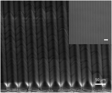 |
| | Fig. 9 Scanning electron microscope (SEM) image of the triangular optical microstructures (∼50 μm side length) produced via our R2R UV-NIL technology. Inset shows a top view of the periodic microstructures, pictured using an optical microscope. The scale bar of the inset is 110 μm. | |
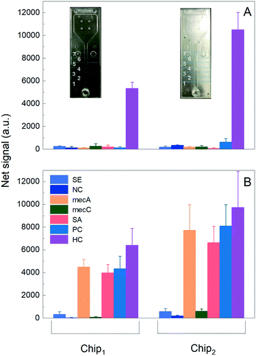 |
| | Fig. 10 Enhancement in the light out-coupling to the photodiodes via R2R UV-NIL produced optical microstructures. The measurements were performed in (A) GENSPEED solution C (as blank measurements) and (B) 1X R2R solution, using the GENSPEED R1 device. Chip1 and Chip2 refer to the test chips without the optical structures and with the optical structures, respectively (shown as insets). In insets, probes of SE to HC were numbered from 1 to 7, respectively. The ss-DNA probes were capillary printed (blue coloured stripes). Each stripe response was demonstrated with a differently coloured column as a mean value ± its standard deviation. For each study, 3 replicates were measured at room temperature using a 20 μL of the corresponding target solution. The biochip photographs were provided as insets. The background values (a.u.) were subtracted from each data to provide a background corrected and integrated net signal (a.u.). | |
4.2. The foil-based biochips
The profilometer measurement revealed 70 μm depth and 2.7 mm width for the fluidic channels of the foil-based chips (Fig. S9 in the ESI†).It could be seen in Fig. 11A that the foil-based DNA chip (i.e., Chip3) showed a clear HC net signal intensity (4484.9 ± 501.6 a.u.) in GENSPEED® solution C (20 μL), used in blank measurements. Due to significantly low negative control signals (i.e., SE, NC, mecA, mecC, SA and PC probes) of the blank solution, a high Rspecific/unspecific value was obtained for HC targets (2.5 nM). For the complete foil-based chips (Chip3), a ∼5-folds higher Rspecific/unspecific was obtained as compared to Chip1. The foil type chips displayed a lower background value therefore lower negative control signals; however specific, HC signal range were same as Chip1 types. The Rspecific/unspecific value was remarkably higher for Chip3, than of the other chip types. As seen in Fig. 11B, the R2R UV-NIL produced foil chips showed clear signals from all expected photodiode regions (i.e., mecA, SA, PC and HC) with 1X R2R solution. Moreover, the CL amount utilised in Chip3 was lower than the ones used in Chip1 and Chip2 (see Table S2, ESI†), due to the chip design difference. In addition, the number of tethered DNA probes is also presumed to be relatively lower in Chip3 as compared to that of Chip1 and Chip2, since the micro-array spotting was applied to obtain smaller biofunctionalised areas within the identically defined stripe outlines. Considering both the effects of the reduced CL amount and the number of DNA probes over the surface, lower specific signals (a.u.) are expected for the foil chip experiments, as compared to Chip1 and Chip2. This hypothesis is confirmed by our results.
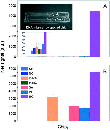 |
| | Fig. 11 High-throughput R2R micro-array spotted ss-DNA foil-chip, with capillary flow channels. The measurements were performed in (A) GENSPEED solution C, as blank measurements. The upper inset shows the photograph of a produced foil-based chip. The spotted ss-DNA probes were numbered from 1 to 7 (i.e., from SE to HC) on the chip. The lower inset shows a closer-look of the negative control (NC) signal region. (B) 1X R2R solution, using the GENSPEED R1 device. Each stripe response was demonstrated with a differently coloured column as a mean value ± its standard deviation. For each study, 3 replicates were measured at room temperature using 20 μL of the corresponding target solution. The background values (a.u.) were subtracted from each data to provide a background corrected and integrated net signal (a.u.). | |
4.3. Dilution studies
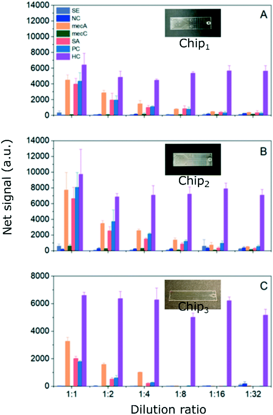
The calibration curves, which were acquired via dilution series studies, were given in Fig. S10 in the ESI.† For both calibration curves, the blank signals (a.u.) measured using GENSPEED® solution C, were excluded from the data since the signals (a.u.) were below the calculated LoB signals (a.u.). From the dilution series study, distinguishable net signals (a.u.) were obtained for all chip types for 0.03, 0.06, 0.13, 0.25, 0.50 and 1.00 μM target mecA concentrations (i.e., from 1:32 to 1:1 dilution factor), provided in Fig. 12. The Chip1 type showed relatively lower net signals (a.u.) for all dilution ratios (Fig. 12A). LoD value for Chip1 was calculated as 0.07 μM. S/N values of Chip1, calculated for dilution factors of 1:4, 1:2 and 1:1, were obtained as 22.9, 35.7 and 261.9, respectively. The serial dilution series study revealed higher Chip2 signals than that of Chip1, for both negative and positive targets (Fig. 12B), with a slightly better LoD of 0.06 μM. By decreasing the LoD value slightly, it was proven that the R2R UV-NIL produced optical microstructures enhances the light out-coupling through the photodiodes thereby pulling down the LoD for specific mecA detection to some extent. S/N values of Chip2, calculated for dilution factors of 1:4, 1:2 and 1:1, were obtained as 38.5, 24.7 and 112.8, respectively. The results showed an increase in the background signal. S/N values of Chip3, calculated for dilution factors of 1:4, 1:2 and 1:1, were obtained as, 307.9, 3337.1 and 380.1 respectively. If only the backgrounds were considered, for instance NC signals (Fig. 12A–C, navy columns), the background intensity was lowest for Chip3 (Fig. 12C), leading highest S/N values.
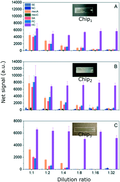 |
| | Fig. 12 Serial dilution studies of the produced chips. (A) Chip1, (B) Chip2 and (C) Chip3 refer to the chips without optical structures, with optical structures and with DNA micro-spots, respectively. For each study, 3 replicates were measured at room temperature. Each stripe response was demonstrated with a differently coloured column as a mean value ± its standard deviation. The experiments were performed with 1:1, 1:2, 1:4, 1:8, 1:16 and 1:32 dilution factors, using 1X R2R solution with 1 μM biotinylated, target mecA solution as the stock. A 20 μl target solution was utilised in each measurement. The background values (a.u.) were subtracted from each data to provide a background corrected and integrated net signal (a.u.). | |
Additionally, there was no linear relationship of the net signal (a.u.) with increasing mecA concentration (μM) for Chip3. Therefore, a correlation could not be obtained. It can also be presumed that the printed sciPOLY3D solution with the ss-DNA probes is reachable by the targets at the PS surface (for Chip1 and Chip2). However, a different DNA immobilisation chemistry is applied at the acrylate based photoresin coated PET surface. Due to the acrylate based chemical structures of the hydrophilic matrix of the sciPOLY3D product and the custom-made photoresin, the product might slightly inter-diffuse into the resin during the immobilisation process resulting in loss of the reachable sites of the ss-DNA probes. Thus, the interaction with the thermoplastic PET polymer and the sciPOLY3D can be significantly lower than of Chip3 case. Due to this reason, chip to chip variations could occur in the foil-based chip type (i.e., Chip3). However; yet, a net signal of 1008.1 ± 34.3 (a.u.) obtained for 0.25 μM target mecA concentration corresponding to 1:4 dilution factor, was far above the hypothetical LoB signal of 42.1 (a.u.). Hence, it is still possible to detect mecA gene with the DNA micro-spotted foil chips, down to a concentration of 0.25 μM, extending in the detection range.
5. Conclusion
The biochips produced with our high-throughput R2R UV-NIL technology (i.e., 4500 biochip parts/hour), demonstrated important results for the clinical detection of the antibiotic resistant MRSA pathogen. With the biochip parts produced via widely used injection-moulding technology, R2R micro-structured chip sections were integrated. The imprinted optical microstructures increased the HC signal by 52.3% besides the rest positive signals, as compared to the injection-moulded chips without optical structures over their surface. S/N and sensitivity increased in the presence of the imprinted optical structures as compared to that of no structure (i.e., planar) case. For the mecA gene detection, LoD value decreased about one percent with the use of the imprinted microstructures with increasing background signals. All these outputs proved that there was an enhancement of the transport of the generated chemiluminescent light towards the photodiodes. Furthermore, in R2R UV-NIL technology, we went one step further and brought in a new perspective for the collective biochip production. With a complete transformation from the injection moulding to the foil-based approach, R2R UV-NIL produced capillary channels were biofunctionalised via a R2R DNA micro-spotting line. The detection of the target mecA concentration down to a concentration of 0.25 μM was possible via the produced foil-based chips. The applied volume of the CL solution (i.e., the GENSPEED® F) in this system is one of the decisive parameters on the net signal (a.u.) levels. Furthermore, while the injection-moulding technology enables production of ∼600 biochips/hour by allowing 5 chip designs per working tool, our approach increases the throughput of microfluidic patterns by a factor of ∼7.5. Therefore, in the light of all these results, we believe that our work brings a new horizon to high-throughput biochip production.
Author contributions
PT, MS, AH, UP, DN, SR, LK, MR, BH, IK, MS, MWT, ML, MH, WW, MS, GB, SH, NO, JK, SK, BS and JH were involved in development of all conceptualisation and methodology steps of this study. PT, BH, IK, CS and SJ were involved in investigation sections. PT done validation and visualization. PT, MS, AH, UP, DN, SR, LK, MR and BH contributed in writing-original draft. PT, MS and JH done writing-review & editing. JH additionally provided supervision for this study.
Conflicts of interest
The authors declare no conflicts of interest.
Acknowledgements
This research was supported by R2R BIOFLUIDICS project (http://www.r2r-biofluidics.eu/) under Horizon 2020 European Union (EU) Research and Innovation Programme with grant agreement no 646260. The research was also partially supported by NextGenMicrofluidics project (https:// www.nextgenmicrofluidics.eu/) under HORIZON2020 with grant agreement no 862092. The authors cordially thank Gerburg Schider & Gerhard Mohr, Markus Postl, Paul Patter and Alexander Wheeldon (JOANNEUM RESEARCH – Materials, Weiz, Austria) for revising the manuscript, preparing all the chip and R2R pilot line illustrations, taking the photographs and providing technical support, respectively. The authors are also grateful to Christian Wolf and Johannes Götz (JOANNEUM RESEARCH – Materials, Weiz, Austria) for their supports in the fluidic design and R2R UV-NIL structuring, respectively. We further kindly thank Alba Simon Munoz and Robert Fay (SCIENION AG, Berlin, Germany) for providing the illustration of the R2R micro-spotting line. PT specially thanks Ege Ozgun (NANOTAM, Bilkent University, Ankara, Turkey) for critically reading the manuscript.
Notes and references
- M. Campas and I. Katakis, TrAC, Trends Anal. Chem., 2004, 23, 49–62 CrossRef CAS.
- D. Shalon, S. J. Smith and P. O. Brown, Genome Res., 1996, 6, 639–645 CrossRef CAS.
- L. Berrade, A. E. Garcia and J. A. Camarero, Pharm. Res., 2011, 28, 1480–1499 CrossRef CAS.
- X. Teng and H. Xiao, Sci. China, Ser. C: Life Sci., 2009, 52, 7–16 CrossRef CAS.
- P. Toren, E. Ozgur and M. Bayindir, Lab Chip, 2016, 16, 2572–2595 RSC.
- S. L. Freire and A. R. Wheeler, Lab Chip, 2006, 6, 1415–1423 RSC.
- S. Spisak, Z. Tulassay, B. Molnar and A. Guttman, Electrophoresis, 2007, 28, 4261–4273 CrossRef CAS.
- P. Zhang, M. He and Y. Zeng, Lab Chip, 2016, 16, 3033–3042 RSC.
- R. Baudoin, A. Corlu, L. Griscom and C. Legallais,
et al.
, Toxicol. In Vitro, 2007, 21, 535–544 CrossRef CAS.
- H. E. Karakas, J. Kim, J. Park and J. M. Oh,
et al.
, Sci. Rep., 2017, 7, 2050 CrossRef.
- A. Niemz, T. M. Ferguson and D. S. Boyle, Trends Biotechnol., 2011, 29, 240–250 CrossRef CAS.
- N. Convery and N. Gadegaard, Microsyst. Nanoeng., 2019, 2, 76–91 Search PubMed.
- M. Leitgeb, D. Nees, S. Ruttloff and U. Palfinger,
et al.
, ACS Nano, 2016, 10, 4926–4941 CrossRef CAS.
- J. Hiltunen, C. Liedert, M. Hiltunen and O. H. Huttunen,
et al.
, Lab Chip, 2018, 18, 1552–1559 RSC.
- R. Liedert, L. K. Amundsen, A. Hokkanen and M. Maki,
et al.
, Lab Chip, 2012, 12, 333–339 RSC.
- S. Murthy, H. Pranov, H. C. Pedersen and R. Taboryski, J. Vac. Sci. Technol., B: Nanotechnol. Microelectron.: Mater., Process., Meas., Phenom., 2016, 34, 06KM02-01–06KM02-07 Search PubMed.
-
B. J. Taniguchi, U. Noriyuki, S. Hidetoshi and M. Jun, et al., Nanoimprint Technology: Nanotransfer for Thermoplastic and Photocurable Polymers, John Wiley & Sons, Ltd, Chichester, UK, 2013, pp. 91–168 Search PubMed.
- S. Y. Chou, P. R. Krauss and P. J. Renstrom, Appl. Phys. Lett., 1995, 67, 3114 CrossRef CAS.
- L. Peng, Y. Deng, P. Yi and X. Lai, J. Micromech. Microeng., 2014, 24, 013001 CrossRef.
- J. Haisma, M. Verheijen, K. V. D. Heuvel and J. V. D. Berg, J. Vac. Sci. Technol., B: Nanotechnol. Microelectron.: Mater., Process., Meas., Phenom., 1996, 14, 4124–4128 CrossRef CAS.
- S. H. Ahn and L. J. Guo, Adv. Mater., 2008, 20, 2044–2049 CrossRef CAS.
- P. Maury, D. Turkenburg, N. Stroeks and P. Giesen,
et al.
, Microelectron. Eng., 2011, 88, 2052–2055 CrossRef CAS.
- P. Yi, C. Zhang, L. Peng and X. Lai, RSC Adv., 2017, 7, 48835–48840 RSC.
- A. V. Shneidman, K. P. Becker, M. A. Lukas and N. Torgerson,
et al.
, ACS Photonics, 2018, 5, 1839–1845 CrossRef CAS.
- N. Kooy, K. Mohamed, L. T. Pin and O. S. Guan, Nanoscale Res. Lett., 2014, 9, 320 CrossRef.
- J. S. Wi, S. Lee, S. H. Lee and D. K. Oh,
et al.
, Nanoscale, 2017, 9, 1398–1402 RSC.
-
B. Stadlober, D. Nees, A. Haase and U. Palfinger, et al., OSA Tech. Digest, 2019, paper OT1A.7 Search PubMed.
-
D. Nees, S. Ruttloff, U. Palfinger and B. Stadlober, Proc. SPIE 9777 Alternative Lithographic Technologies VIII, 2016, vol. 97770D Search PubMed.
- P. Toren, M. Smolka, A. Haase and S. Ruttloff,
et al.
, Eur. J. Mater. Sci. Eng., 2020, 5, 11–16 CAS.
- M. Smolka, S. Ruttloff, D. Nees and C. Prietl,
et al.
, Proceedings, 2018, 2, 1054 CrossRef.
- J. Chen, Y. Zhou, D. Wang and F. He,
et al.
, Lab Chip, 2015, 15, 3086–3094 RSC.
- P. Gastmeier, F. Schwab, M. Behnke and C. Geffers, Antimicrob. Resist. Infect. Control, 2012, 1, 3 CrossRef.
- Y. Utsui and T. Yokota, Antimicrob. Agents Chemother., 1985, 28, 397–403 CrossRef CAS.
- K. Ubukata, R. Nonoguchi, M. Matsuhashi and M. Konno, J. Bacteriol., 1989, 171, 2882–2885 CrossRef CAS.
- E. M. Harrison, G. K. Paterson, M. T. Holden and J. Larsen,
et al.
, EMBO Mol. Med., 2013, 5, 509–515 CAS.
- T. Ito, K. Hiramatsu, A. Tomasz and H. de Lencastre,
et al.
, Antimicrob. Agents Chemother., 2012, 56, 4997–4999 CAS.
- L. Garcia-Alvarez, M. T. Holden, H. Lindsay and C. R. Webb,
et al.
, Lancet Infect. Dis., 2011, 11, 595–603 CrossRef CAS.
- C. Kim, C. Milheirico, S. Gardete and M. A. Holmes,
et al.
, J. Biol. Chem., 2012, 287, 36854–36863 CrossRef CAS.
- H. de Lencastre, B. L. de Jonge, P. R. Matthews and A. Tomasz, J. Antimicrob. Chemother., 1994, 33, 7–24 CrossRef CAS.
- Z. Li and T. Feizi, FEBS Lett., 2018, 592, 3976–3991 CrossRef CAS.
-
E. J. Septimus, Infect. Prevention, Springer, Cambridge, 2018 Search PubMed.
- G. Gingras, M. H. Guertin, J. F. Laprise and M. Drolet,
et al.
, PLoS One, 2016, 11, e0163880 CrossRef.
- L. McKinley, B. Becerra, H. Moriarty and T. H. Short,
et al.
, Am. J. Infect. Control, 2016, 44, 1047–1049 CrossRef.
- S. D. Braun, S. Monecke, A. Thurmer and A. Ruppelt,
et al.
, PLoS One, 2014, 9, e102232 CrossRef.
- A. Petersen, A. Medina and A. R. Larsen, APMIS, 2015, 123, 478–481 CrossRef CAS.
- H. Soderlund, Ann. Biol. Clin., 1990, 48, 489–491 CAS.
- V. Mazet, C. Carteret, D. Brie and J. Idier,
et al.
, Chemom. Intell. Lab. Syst., 2005, 76, 121–133 CrossRef CAS.
- D. A. Armbruster and T. Pry, Clin. Biochem. Rev., 2008, 29(Suppl 1), S49–S52 Search PubMed.
- A. Forootan, R. Sjöback, J. Björkman and B. Sjögreen,
et al.
, Biomol. Detect. Quantif., 2017, 12, 1–6 CrossRef CAS.
Footnotes |
| † Electronic supplementary information (ESI) available: GENSPEED® system, our R2R micro-spotting line, data related with the produced biochips. Supplementary movies available: [R2R DNA micro spotting, capillary flow in the R2R UV-NIL produced biochips]. See DOI: 10.1039/d0lc00751j |
| ‡ Current address: ERBA Diagnostics Mannheim GmbH, 68219 Mannheim, Germany. (Web: www.erbamannheim.com). |
| § Where PS, PET, PEEK, PP and PEN refer to polystyrene, polyethylene terephthalate, polyether ether ketone, polypropylene and polyethylene naphthalate, respectively. |
| ¶ Maximum reachable web speed is 30 m min−1. |
|
| This journal is © The Royal Society of Chemistry 2020 |
Click here to see how this site uses Cookies. View our privacy policy here. 
 Open Access Article
 This Open Access Article is licensed under a Creative Commons Attribution-Non Commercial 3.0 Unported Licence
 *a,
Martin
Smolka
a,
Anja
Haase
a,
Ursula
Palfinger
a,
Dieter
Nees
*a,
Martin
Smolka
a,
Anja
Haase
a,
Ursula
Palfinger
a,
Dieter
Nees