
 Open Access Article
 This Open Access Article is licensed under a
 Creative Commons Attribution 3.0 Unported Licence
Hollow silicon microneedle fabrication using advanced plasma etch technologies for applications in transdermal drug delivery
Chris J. W.
Bolton
 *ab,
Olivia
Howells
b,
Gareth J.
Blayney
b,
Pey F.
Eng
c,
James C.
Birchall
d,
Benedetta
Gualeni
d,
Kerry
Roberts
a,
Huma
Ashraf
a and
Owen J.
Guy
b
*ab,
Olivia
Howells
b,
Gareth J.
Blayney
b,
Pey F.
Eng
c,
James C.
Birchall
d,
Benedetta
Gualeni
d,
Kerry
Roberts
a,
Huma
Ashraf
a and
Owen J.
Guy
b
aSPTS Technologies, Ringland Way, Newport, NP18 2TA, UK. E-mail: chris.bolton@spts.com
bCollege of Engineering, Swansea University, Swansea, SA2 8PP, UK
cBioMEMS Technologies, Cardiff, UK
dSchool of Pharmacy and Pharmaceutical Sciences, Cardiff University, Cardiff, CF10 3NB, UK
First published on 7th July 2020
Abstract
A novel production process flow is presented here for the manufacture of hollow silicon microneedles using deep reactive-ion etching (DRIE) technology. The patent-pending three-step process flow has been developed to produce multiple arrays of sharp-tipped, hollow microneedles, which facilitate easy insertion and controlled fluid injection into excised skin samples. A bevelled tip and vertical sidewalls for the microneedle have been achieved with good uniformity, despite >45% open etch area. Processing steps and etch challenges are discussed, and preliminary skin testing results are presented, showing effective needle insertion and delivery of fluorescent dye into ex vivo skin from human breast tissue.
Introduction
Microneedles (MN) are becoming increasingly popular in biomedical applications for several reasons: transdermal insertion is regarded as painless and minimally invasive, compared to traditional hypodermic needles;2,3 reduced discomfort and fear of injection among patients;2–4 reduced risk of infection.5,6 Microneedles do not have the same potential for physical or infectious harm presented by conventional hypodermic needles, and therefore use of hollow microneedles in place of hypodermics would significantly decrease the risk of sharps injuries to medical professionals.4,7–10Microneedles are typically constructed from plastic,11,12 metal13 or silicon.14 Examples of hollow plastic needles are available,11 however the majority of commercially available polymer microneedles remain solid due to the difficulty involved with integrating the bore.12,15,16 The plastic moulding process also restricts flexibility in the design whereas dry silicon etching allows for tailoring of processes to individual applications, for example needle length to target different skin depths.
Metal MNs are expensive to produce17 and it has proven difficult to machine hollow metal MNs in a cost effective production process. In terms of width dimensions, the 32G hypodermic needle is similar to the hollow silicon microneedles presented here, but the risk associated with the much increased length of the hypodermic requires continuous training programmes in order to be handled safely,18,19 and their use results in more pain compared to microneedles.3
Hollow bevelled silicon microneedles have been demonstrated,14 but in general their fabrication either relies heavily on wet chemicals such as KOH or HF for the creation of the bevelled surface,14,20–22 or plasma etching of the bevel surface results in an unconventional needle shape.14,23
Advancements in dry etching technologies have made it possible to develop a manufacture process flow that produces repeatable silicon hollow bevelled microneedles.24
The novel process flow here benefits from the avoidance of hazardous wet chemicals while maintaining a recognisable and easily used needle shape. Additionally, the nature of the semiconducting material further permits the future development of an all-in-one diagnostic and therapeutic (theranostic) device.25 Metal plating and dielectric deposition on silicon means that a sensing microchip device with the additional capability of administering medicines in relation to data input from the MN sensor could be developed.25
Hollow microneedles hold a key advantage over the multitude of available ‘solid’ microneedles; the ability to inject a controlled dose. Solid microneedles do not give the same benefit of pressured sub-dermal injection of fluids, and instead rely on the passive diffusion of fluid through previously created holes.12 This method is adequate for the cosmetics industry,26 but does not deliver the precision needed for state of the art medical applications. Additionally, the bevelled tip of the microneedle decreases the insertion force required to break through a patient's stratum corneum, reducing discomfort and potential issues with in situ breakage due to application force.2,23,27
The primary focus of this article is to present a novel process flow for the fabrication of hollow silicon microneedles, exclusively using dry plasma processing techniques. In addition to this, the results of a number of proof of concept experiments are presented to show effective insertion and injection of the MNs. However, at this stage these biological tests are not intended to be comprehensive and will be expanded upon in future studies.
Method
Etching and photolithography
Silicon wafers were purchased from Si-mat (Silicon Materials, Germany) while photolithography resists and developer were purchased from Microchemicals GmbH. Etching steps were performed on a SPTS Technologies DSi-v RF plasma processing chamber (Fig. 1).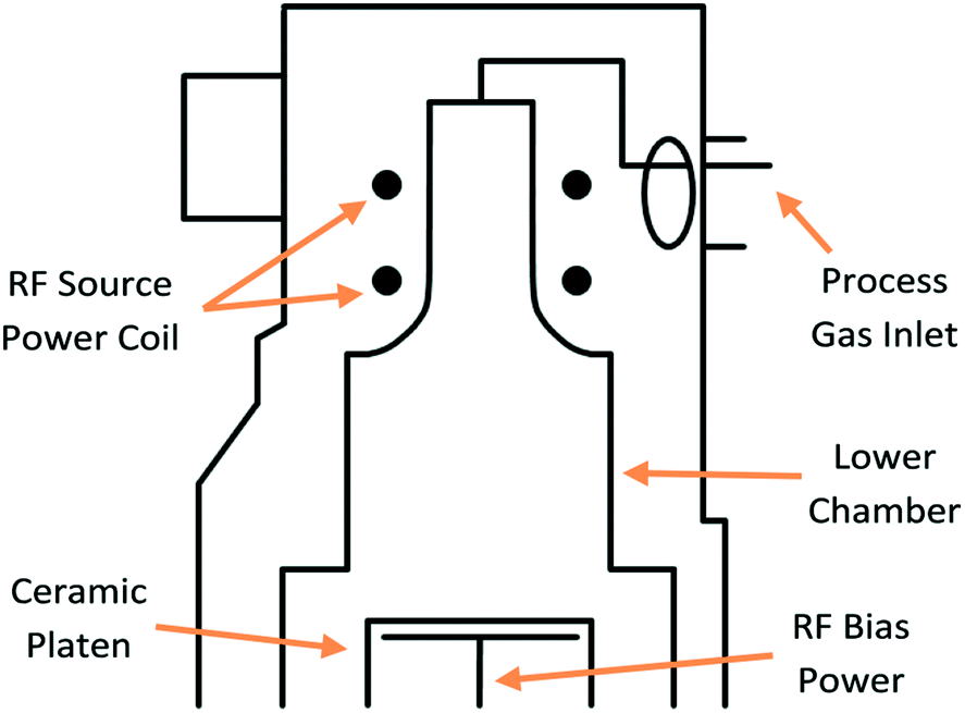 | ||
| Fig. 1 Cross-section of SPTS Technologies Ltd DSi-v plasma etch chamber. The central gas inlet leads to a low volume chamber for plasma etching of silicon substrates. | ||
A Laurell WS-650 spin coater was used to coat the wafers with AZ125 NXT photoresist for the bevel and bore patterning process, while a SUSS MicroTec AS8 spray coater was used to deposit AZnLof2070 photoresist for the microneedle shaft patterning. Photolithography resist patterning was hardened using a SUSS MicroTec MA8 UV mask aligner that allows backside alignment. Once patterned, wafer masking was completed using AZ276 developer.
Characterisation
Proof of concept microneedle penetration characterisation was performed using either full thickness porcine skin (Wetlab Ltd. Warwicks, UK) or post-surgical human breast tissue (under full ethical approval and informed patient consent, local research ethics committee reference 08/WSE03/55). Methylene blue, FITC-insulin and DIL (1,1′-dioctadecyl-3,3,3′,3′-tetramethylindocarbocyanine perchlorate), used for characterisation of skin penetration efficacy, were purchased (Sigma-Aldrich, Dorset, UK). An axial compression analyser (Hounsfield/Tinius Olsen H1-KS, PA, USA) was used for mechanical testing. Imaging was performed using fluorescent microscopy (Zeiss Axio Imager M1, Germany) and ImageJ software (Version 1.51k, National Institutes of Health, MD, USA).Plasma etch processing
A high density, inductively coupled plasma etch system was used to etch the silicon for microneedle production. Due to the requirements of the etched features the selected module was a DSi-v from SPTS Technologies Ltd (Fig. 1). In this tool, the gas enters the chamber thorough a central gas feed before being excited to form a plasma using an RF coil around the top chamber section. The plasma diffuses into the lower chamber, which has a smaller volume compared to other DRIE (deep reactive ion etching) machines, reducing the plasma residence time. Lower residence time leads to a more effective etch step, keeping larger features clean and free from process-induced defects – which is critical for the production of silicon microneedles. The wafer sits on a ceramic platen in the chamber and is electrostatically clamped, allowing it to be cooled by flowing helium to the backside of the substrate. RF bias is applied to the platen to accelerate ions towards the wafer surface, facilitating the physical element of DRIE.The MN features were etched on die sizes typically 1.7 mm × 7.5 mm, located on a 100 mm diameter wafer. The 100 mm device wafers were carried on a 150 mm substrate, allowing future development of a scalable process for larger (150 mm diameter) wafers. Etched features were analysed using a scanning electron microscope (SEM), to characterise and quantify critical dimensions, surface roughness, and etch quality.
Fabrication steps
The novel process flow for dry etch silicon microneedle fabrication (Fig. 2) consists of three main parts: the bevel creation for the angled sharp MN tip [(A) or steps (a) to (c)]; the central bore etch, used for fluid transport within the MN [(B) or steps (d) to (f)]; and the shaft etch, to determine the length and consequently skin penetration depth [(C) or steps (g) to (i)]. Photolithography steps were developed at the Centre for Nanohealth, Swansea University, using AZ125 NXT photoresist resist for steps (a) and (d) and spray coated AZnLof2070 photoresist for step (g). Although this process flow is designed for the manufacture of hollow microneedles, solid microneedles can also be produced by simply removing step (B) from the fabrication sequence.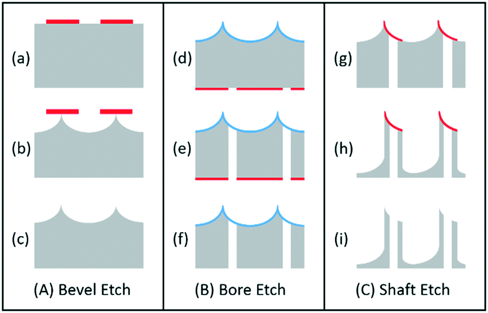 | ||
| Fig. 2 Process flow for hollow silicon microneedle production, patent pending.1 Silicon wafers are shown in grey, with photoresist masks and oxide stop layers shown in red and blue respectively. | ||
Dry etch processes
Single step etch
Step (b) in the process flow (Fig. 2) is the creation of the sloped surface required for the bevel of the microneedle. To achieve this, a single step etch was setup whereby vertical and lateral etching takes place in addition to simultaneous passivation. In this case, platen RF bias applied during the process provided ion bombardment to the base surface of the feature.24 This physical assistance gave the etch some directionality under conditions that would otherwise lead to an isotropic etch form. This partial directionality during the isotropic etch enabled tuning of the bevel angle and resulted in the desired shape for microneedle bevel production.Switched processing
Traditional switched etching consists of two steps, a polymer deposition (typically consisting of C4F8) and an etch step. Anisotropic 2-step DRIE protects the sidewall with the deposition step, and then selectively etches the base of the feature before returning to the deposition step, a sequence known as the Bosch process.28 More recent switched etching techniques are similar but commonly manifest as a three step process (shown in Fig. 3), consisting of a polymer deposition step (Dep; panel 2), a deposition removal step (etch 1, E1; panel 3), and a silicon etch step (etch 2, E2; panel 4). While the separation of the etch step into E1 and E2 adds to the complexity of the process, it also allows both steps to be more effective. The base deposition is removed more quickly by a physical E1, and the silicon is etched faster in the chemical E2 to increase the overall process etch rate. The separation of steps also has benefits in base roughness, as the base deposition is cleared (with SF6, O2 or an SF6/O2 combination) before the dedicated etching of Si with SF6 begins. The cyclical repetition of steps (panels 5–7) produces a directional anisotropic etch with close to vertical sidewalls (panel 8), ideal for steps (e) and (h) of the microneedle process flow (Fig. 2).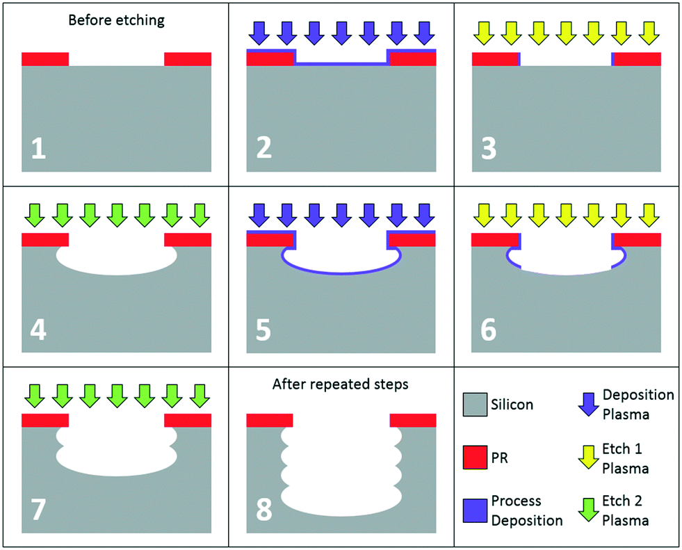 | ||
| Fig. 3 3-Phase switched etching, illustrated step-by-step. | ||
Process challenges
Results
Uniformity improvements
For the three etch stages shown in Fig. 2, the etch depth uniformity was a particular challenge for the bevel (b) and shaft (h) steps, as these were performed on patterns with >45% total open area. To control the uniformity of these applications, mask sets were designed whereby excess silicon was available around the edge of the wafer. In the case of the bevel etch (b), this change, in addition to process recipe optimisations of 25% RF power increase and 10 mT pressure decrease, resulted in the etch depth uniformity improving from >±11% to <±4% (Fig. 4). This exceeds the uniformity expectation for a wafer with a pattern of this open area and increases the number of usable die per wafer. A similar improvement was also applied to the shaft etch (h), which was optimised for depth uniformity <±3%.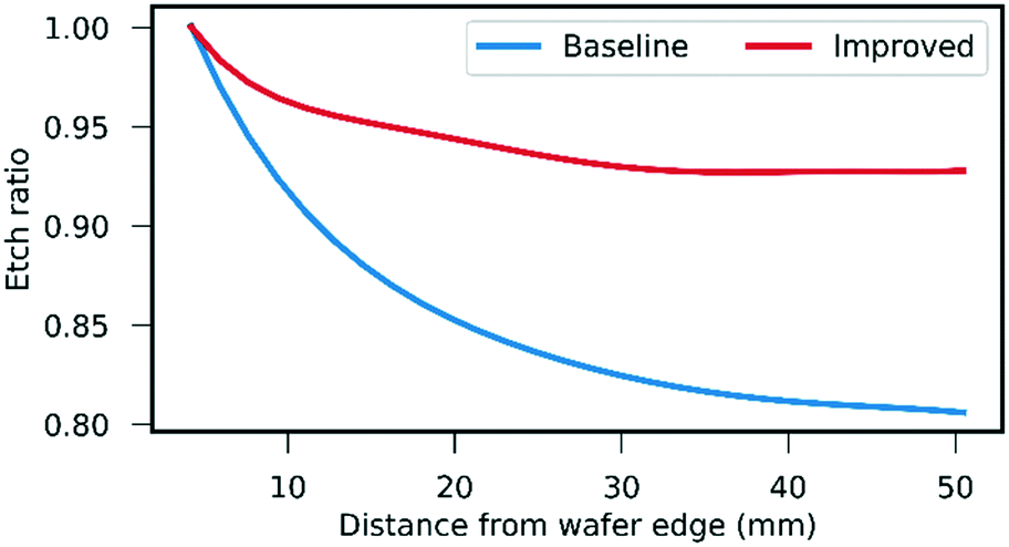 | ||
| Fig. 4 Graph comparing etch depths from edge to centre of wafer, before and after improvements. | ||
Bevel etch
A peaked profile was achieved by undercutting the PR mask with a single step dry etch process using SF6, C4F8, and O2 with a flow ratio approximately 6![[thin space (1/6-em)]](https://www.rsc.org/images/entities/char_2009.gif) :1:1 at 70 mTorr chamber pressure. 2500 W RF power was applied with the source coil, and 40 W was used for the RF bias to the platen. Process results are shown in Table 1.
:1:1 at 70 mTorr chamber pressure. 2500 W RF power was applied with the source coil, and 40 W was used for the RF bias to the platen. Process results are shown in Table 1.
| Parameter (units) | Bevel | Bore | Shaft |
|---|---|---|---|
| Depth (μm) | 500 | 1157 | 790 |
| Etch rate (μm min−1) | 8.5 | 8.1 | 6.2 |
| Profile (°) | ∼20.0 | 89.5 | 89.0 |
| Selectivity (Si:PR) |
90 | 16 | 74 |
| Uniformity (±%) | 4.0 | 1.1 | 2.2 |
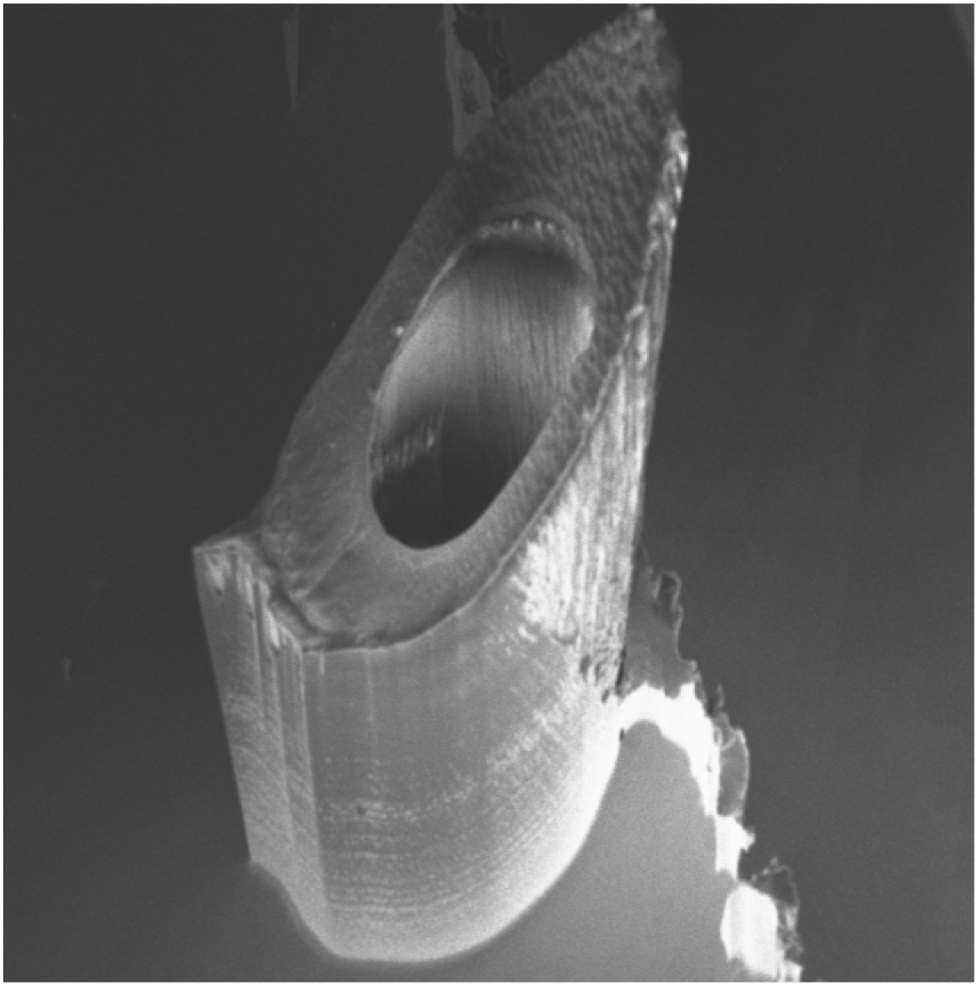
Profile control is essential to produce the angled tip of the needle. Pressure and platen bias were used to control the level of anisotropy for this etch,24 and a favourable angle of ∼20° (Fig. 5) was thus created for the sharp MN tip, which reduces the insertion force required.27 As well as limiting the mechanical strain on the microneedle upon insertion, the lower force needed to penetrate skin due to the ∼20° tip results in less pain for patients.2,27 In other examples of silicon microneedles, the needle tip is fabricated using a chemical wet etch after the creation of the bore,14,22 which can compromise bore quality and ultimately limits the final microneedle shapes that can be produced. Processing the needle tip by dry etching allows the bore and shaft to be defined afterwards, thus avoiding wet chemicals and associated process complications.
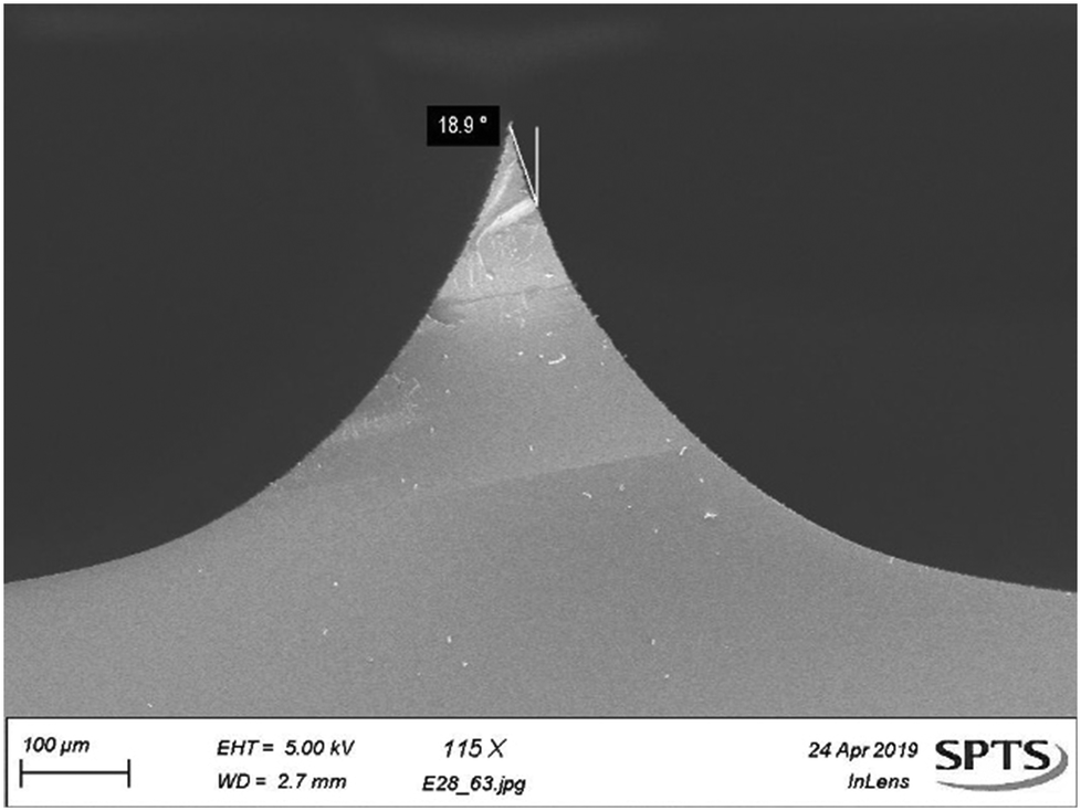 | ||
| Fig. 5 SEM image showing bevel-etched sharp tip for microneedles. | ||
Bore etch
After being removed from the wafer carriers, bevelled wafers were patterned for the bore step. This included a stop layer on the bevel surface, shown in Fig. 2. Once patterning is completed, wafers are rebonded to the carrier substrate with the backside up to allow for the etching of the bore. While bonded in this configuration, the bevels are protected from damage by protrusions that prevent the sharp tips from bearing weight. Fig. 6 shows a deep TSV etch demonstrated on thick test wafers achieving 1157 μm depth with a via CD of 100 μm using the 3-step switched process described above. The Dep, E1, and E2 steps consisted of 450 sccm C4F8, 200/100 sccm O2/SF6, and 720 sccm SF6, respectively. Across the total process length, step times, chamber pressure, and platen RF bias values were all varied to maintain a vertical etch profile.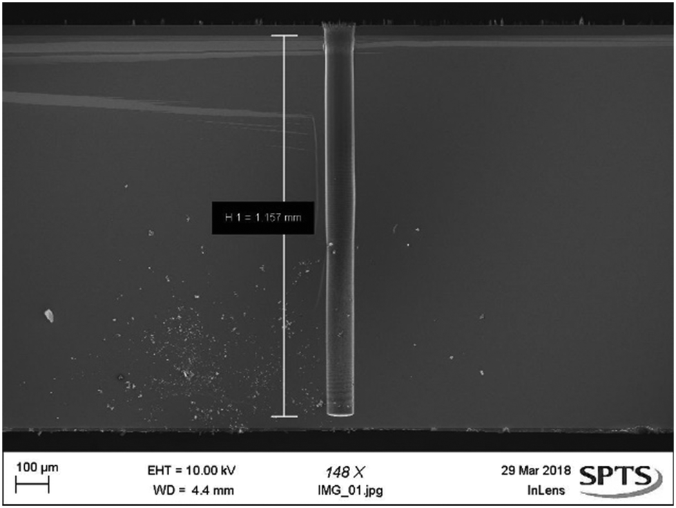 | ||
| Fig. 6 SEM image showing bore, etched to a depth of 1157 μm on a test wafer for fluid or cell transport. | ||
The AR of the bore is in line with current industrial processes at >11:1,24,29 however, the depth presented here represents a significant increase on previously demonstrated etches in terms of absolute depth with a circular TSV. 1157 μm is also deeper than ‘Ultra Deep Reactive Ion Etch’ (UDRIE) processes performed on trenches of a similar CD, despite TSV's having limited species transport to the base of the feature compared to trenches and therefore presenting additional AR,24 etch rate, and depth challenges.30
Previously mentioned AR dependent effects24 were eliminated by balancing Dep and E2 step times and pressures to minimise damage to the feature, which produced a high quality etch result, exceeding the depth required for MN production. The straight profile does not restrict fluid movement along the bore, while smooth sidewalls aid in limiting turbulent flow and maintained cell viability in cell delivery studies.31
Shaft etch
The shaft etch (Fig. 7) resulted in >89° pillar angle to a depth of 790 μm. This was completed with medium source RF powers and low chamber pressure in all three steps. The gas flows were 360 sccm C4F8, 320 sccm SF6, and 315 sccm SF6 for Dep, E1, and E2 respectively. During the E1 and E2 steps, platen RF bias was applied with 112 W and 36 W respectively; this aids in maintaining a straight sidewall to the microneedle. The achieved profile is key in maintaining mechanical rigidity of the MN; too narrow at the base and the wall thickness between the outside of the microneedle and the central bore becomes a possible fracture point.27 This shape would also introduce the issue of an ‘arrowhead’ profile to the microneedle, which is more likely to become lodged in a patient's skin.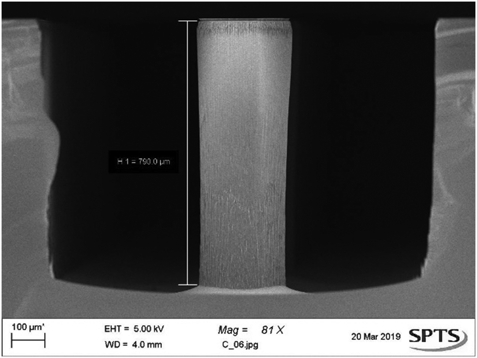 | ||
| Fig. 7 SEM image showing the shaft, etched for microneedle length of 790 μm on a test wafer. | ||
Device integration
Fig. 8 shows the combination of the bore etch (Fig. 2e) with the bevel etch (Fig. 2b). Additionally, the bevel (Fig. 2b) and shaft (Fig. 2h) etches can be combined to produce solid microneedles which can be used for insertion testing, as the force required is the same for microneedles with or without the central bore.27 The integration of the bore with the solid needles offers no further process complications (Fig. 9).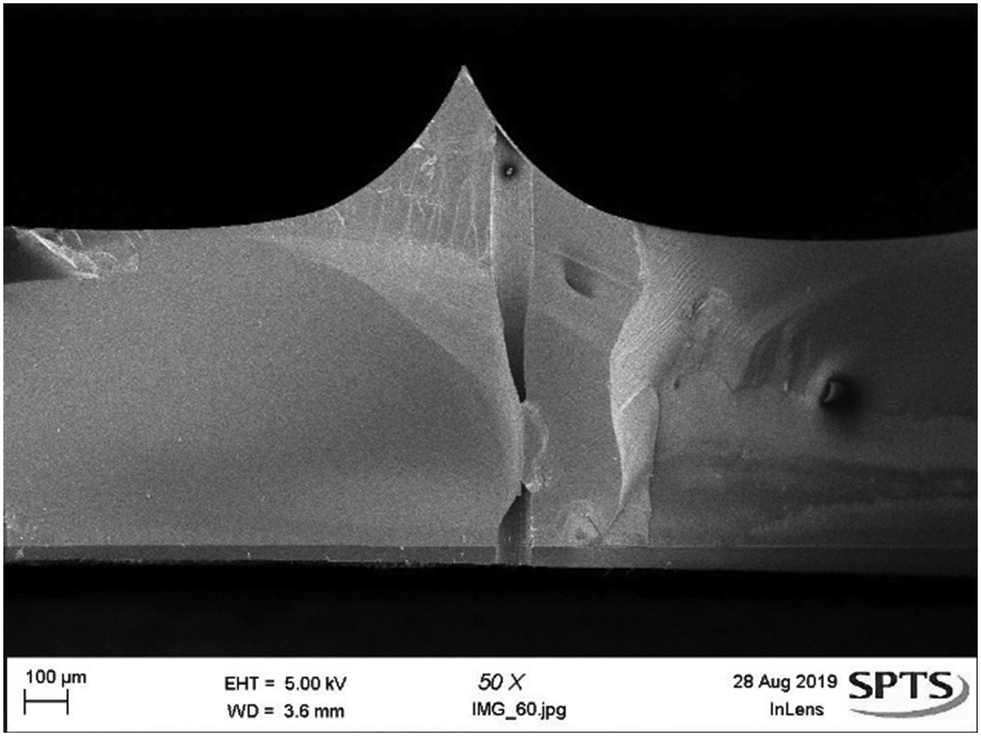 | ||
| Fig. 8 SEM image showing the bore etch performed on a bevel surface. The bore transfers to bevel wafers with no issues, stopping on a backside layer. | ||
 | ||
| Fig. 9 Silicon microneedle with central bore.1 | ||
The three processes in combination are used to fabricate a hollow microneedle that can be produced in variable lengths, depending on application. The MN die are then singulated and mounted to syringe adaptors for delivery applications, or coated with metals to create electrodes for theranostic use.25
Further improvements to the etch quality could be made with optimisation of the masking and lithography steps. Patterning PR on an angled surface such as the bevel introduces unique challenges, where any PR defects present on the wafer surface results in roughness and isolated silicon spikes during the etch. Within the current patterning regime, the microneedle etch has been optimised to reduce these effects by increasing the time of the shaft etch E2 step to undercut any defects present on the bevel surface, minimising roughness in the final device.
Delivery through hollow microneedles
Mechanical testing
Axial compression tests (n = 3) were performed on 1 × 5 MN arrays using a Hounsfield/Tinius Olsen compression analyser (model H1-KS). A 50 N load cell enabled the compression platform to descend, exerting an increasing force on the MNs at a fixed rate of 4.5 mm s−1 to determine the point of fracture. The analyser detected several MN fractures over a compression distance of 250–400 μm, which is attributable to each of the 5 MNs breaking over different compression distances. The results indicate that the MN arrays withstand a maximum force of 22 N before completely fracturing, showing that a MN array has sufficient mechanical strength to resist fracture upon thumb pressure insertion, which is deemed to be <10N.32 Furthermore, as the compression platform is composed of hard metal with little elasticity or movement, it is likely that the MN will be able to withstand a greater force upon penetration through the softer, elastic skin.Insertion testing
Proof of concept experiments were conducted using 1 × 5 microneedle arrays. A single array was glued to a syringe adaptor that was attached to a syringe via a Luer-lock (Fig. 11, Right). To determine whether the microneedles were sharp enough to penetrate through the stratum corneum, methylene blue staining was conducted, following insertion of MNs. Methylene blue is a hydrophilic, low molecular weight molecule that cannot diffuse through the hydrophobic stratum corneum independently. Any exposure of the hydrophilic viable cells beneath the stratum corneum would stain blue, indicating that the stratum corneum had been breached.33 Microneedles were inserted into porcine skin (Wetlab Ltd. Warwicks, UK) via thumb pressure, stained with methylene blue (Sigma-Aldrich, Dorset, UK) for five minutes and washed with ethanol wipes. Fig. 10 shows visual confirmation of the penetration of all five microneedles. | ||
| Fig. 10 Visual skin penetration efficiency of 1 × 5 microneedle array, stained with methylene blue. Imaged with a Samsung A70 (2019) smartphone. | ||
Skin penetration and fluid flow
To demonstrate microneedle penetration depths, optical coherence tomography (OCT) on excised human breast tissue (local research ethics committee reference 08/WSE03/55) was performed (Fig. 11, Left). The OCT image clearly shows an insertion profile, characteristic of a bevelled tip microneedle, illustrating efficient microneedle penetration through the stratum corneum. The total length of the microneedle pre-penetration measured 700 μm, however, the OCT indicated the microneedle formed an insertion channel profile of at least 400 μm–57% of the original length. At this penetration depth, it was confirmed that the bore of the microneedle was fully inserted beneath the stratum corneum and into the epidermis. Depth measurements were extracted using ImageJ software.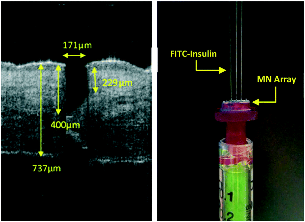 | ||
| Fig. 11 Left; OCT imaging of excised human breast skin after the application of a silicon microneedle. Right; FITC-insulin injection through hollow microneedles attached to a syringe, imaged with a Samsung A70 (2019) smartphone. | ||
Testing of hollow microneedles for their injection potential was conducted using FITC-labelled insulin that fluoresces under UV (ultraviolet) light. Fig. 11 (Right) demonstrates a microneedle adaptor Luer-locked to a syringe. Upon applying thumb pressure to the syringe plunger, straight, consistent liquid jets were produced, indicating FITC-insulin (Sigma-Aldrich, Dorset, UK) was able to flow easily through the microneedle bores of three out of five microneedles. The lack of flow in the two other microneedles was due to adhesive blocking the bore.
Transdermal fluid injection
To confirm the capability of the microneedles for injection into porcine skin, a syringe was loaded with DIL fluorescent dye (Sigma-Aldrich, Dorset, UK) and attached to a syringe pump; a constant flow rate of 10 μl min−1 was applied. 10 μl of DIL was injected into porcine skin and the sample immediately frozen in liquid nitrogen. Skin was then sectioned vertically to a thickness of 8 μm using a cryostat (Leica, Milton Keynes, UK) to visualise the microneedle insertion profile and dye staining of the skin tissue surrounding the injection site.The micrograph (Fig. 12) shows a microneedle insertion channel with a strongly fluorescent region at the apex of where the MN was injected; this area fluoresces at the emission wavelength 565 nm characteristic of DIL. As the dye is highly concentrated at the base of the micro insertion channel, this confirms the dye is injected via microneedle penetration and not introduced through natural skin conduits. The dye did not leak out over the microchannel cavity and was retained at the base; this suggests that hollow silicon microneedles are suitable for transdermal injection and facilitate delivery of substances including pharmaceutical compounds into epidermal and dermal skin layers.
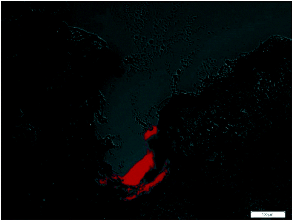 | ||
| Fig. 12 Histology cross section of microneedle microchannel with DIL fluorescent dye injection. | ||
Conclusions
The microneedles produced by the novel manufacture flow (Fig. 2) presented here offer significant advantages over other injection methods currently available. The sub-millimetre construction limits the risk of injury4,7–10 and reduces pain in patients via facile injection,2–4 potentially countering patient phobia of hypodermic needle use.2,34 In addition to the benefits over conventional hypodermic injection, the hollow bevelled silicon microneedle allows for greater versatility than other microneedles. Forced injection through the centre TSV (bore) allows for controlled fluid volume delivery, whilst the sharp bevelled tip limits pain for patients by reducing insertion force.2,27 In addition, the semiconducting base material introduces a pathway to future theranostic device chips.25Conflicts of interest
There are no conflicts of interest to declare.Acknowledgements
Funding provided by EPSRC EP/L020734/1, Welsh Government Smart Expertise “ASSET”, Knowledge Economy Skills Scholarships (KESS), a pan-Wales higher level skills initiative led by Bangor University on behalf of the HE sector in Wales. It is part funded by the Welsh Government's European Social Fund (ESF) convergence programme for West Wales and the Valleys.References
- K. Roberts, H. Ashraf and P. F. Eng, EP3415465A1, 2018 Search PubMed.
- H. S. Gill, D. D. Denson, B. A. Burris and M. R. Prausnitz, Clin. J. Pain, 2010, 24, 585–594 CrossRef PubMed.
- S. Kaushik, A. H. Hord, D. D. Denson, D. V. McAllister, S. Smitra, M. G. Allen and M. R. Prausnitz, Anesth. Analg., 2001, 92, 502–504 CrossRef CAS.
- M. R. Prausnitz, J. A. Mikszta, M. Cormier and A. K. Andrianov, Curr. Top. Microbiol. Immunol., 2009, 333, 369–393 CAS.
- R. F. Donnelly, T. R. R. Singh, M. M. Tunney, D. I. J. Morrow, P. A. McCarron, C. O'Mahony and A. D. Woolfson, Pharm. Res., 2009, 26, 2513–2522 CrossRef CAS PubMed.
- E. M. Vicente-Perez, E. Larrañeta, M. T. C. McCrudden, A. Kissenpfennig, S. Hegarty, H. O. McCarthy and R. F. Donnelly, Eur. J. Pharm. Biopharm., 2017, 117, 400–407 CrossRef CAS PubMed.
- J. I. Blenkharn, British Journal of Nursing, 2009, 18, 860–864 CrossRef PubMed.
- Managing the Risk of Sharps Injuries, NHS Employers, 2015 Search PubMed.
- C. Cooley and J. Gabriel, Nursing Times, 2004, vol. 100, pp. 28–29 Search PubMed.
- S. Q. Wilburn and G. Eijkemans, Int. J. Occup. Environ. Health, 2004, 10, 451–456 CrossRef PubMed.
- I. Mansoor, U. O. Hafeli and B. Stoeber, J. Microelectromech. Syst., 2012, 21, 44–52 CAS.
- D. Duan, C. Moeckly, J. Gysbers, C. Novak, G. Prochnow, K. Siebenaler, L. Albers and K. Hansen, Curr. Drug Delivery, 2011, 8, 557–565 CrossRef CAS PubMed.
- S. P. Davis, W. Martanto, M. G. Allen and M. R. Prausnitz, IEEE Trans. Biomed. Eng., 2005, 52, 909–915 CrossRef PubMed.
- Y. Li, H. Zhang, R. Yang, Y. Laffitte, U. Schmill, W. Hu, M. Kaddoura, E. J. M. Blondeel and B. Cui, Microsyst. Nanoeng., 2019, 5, 11 CrossRef PubMed.
- P. Janphuang, M. Laebua, C. Sriphung, P. Taweewat, A. Sirichalarmkul, K. Sukjantha, N. Promsawat, P. Leuasoongnoen, S. Suphachiaraphan, K. Phimol, D. Isarakorn and S. Tancharakorn, presented in part at the ICEAST 2018, 2018 Search PubMed.
- J.-H. Oh, H.-H. Park, K.-Y. Do, M. Han, D.-H. Hyun, C.-G. Kim, C.-H. Kim, S. S. Lee, S.-J. Hwang, S.-C. Shin and C.-W. Cho, Eur. J. Pharm. Biopharm., 2008, 69, 1040–1045 CrossRef CAS PubMed.
- E. García-López, H. R. Siller and C. A. Rodríguez, presented in part at the 46th SME North American Manufacturing Research Conference, NAMRC 46, Texas, USA, 2018 Search PubMed.
- S. Ahmad, A. Ghani, A. Yaqoob and O. Singh, Int. J. Curr. Res. Rev., 2017, 9, 24–29 Search PubMed.
- M. C. Ottino, A. Argentero, P. A. Argentero, G. Garzaro and C. M. Zotti, BMJ Open, 2019, 9, 1–8 CrossRef PubMed.
- P. Jurcicek, H. Zou, S. Zhang and C. Liu, Micro Nano Lett., 2013, 8, 78–81 CrossRef CAS.
- H. Kim, L. S. Theogarajan and S. Pennathur, J. Micromech. Microeng., 2018, 28, 035007 CrossRef.
- H. J. G. E. Gardeniers, R. Luttge, E. J. W. Berenschot, M. J. D. Boer, S. Y. Yeshurun, M. Hefetz, R. V. T. Oever and A. V. D. Berg, J. Microelectromech. Syst., 2003, 12, 855–862 CrossRef.
- P. Khanna, K. Luongo, J. A. Strom and S. Bhansali, J. Micromech. Microeng., 2010, 20, 045011 CrossRef.
- B. Wu, A. Kumar and S. Pamarthy, J. Appl. Phys., 2010, 108, 051101 CrossRef.
- S. Jeelani, R. C. J. Reddy, T. Maheswaran, G. S. Asokan, A. Dany and B. Anand, J. Pharm. BioAllied Sci., 2014, 6, 6–8 CrossRef PubMed.
- M. T. C. McCrudden, E. McAlister, A. J. Courtenay, P. González-Vázquez, T. Raghu, R. Singh and R. F. Donnelly, Exp. Dermatol., 2015, 24, 561–566 CrossRef PubMed.
- S. P. Davis, B. J. Landis, Z. H. Adams, M. G. Allen and M. R. Prausnitz, J. Biomech., 2004, 37, 1155–1163 CrossRef PubMed.
- F. Laermer and A. Schilp, US5501893A, 1994.
- M. Motoyoshi, Proc. IEEE, 2009, 97, 43–48 CAS.
- Y. Tang, A. Sandoughsaz and K. Najafi, presented in part at the 2017 IEEE 30th International Conference on Micro Electro Mechanical Systems (MEMS), Las Vegas, NV, 2017 Search PubMed.
- B. Gualeni, S. A. Coulman, D. Shah, P. F. Eng, H. Ashraf, P. Vescovo, G. J. Blayney, L.-D. Piveteau, O. J. Guy and J. C. Birchall, Br. J. Dermatol., 2018, 178, 731–739 CrossRef CAS PubMed.
- S. Sharma, A. Saeed, C. Johnson, N. Gadegaard and A. E. Cass, Sens. Biosensing Res., 2017, 13, 104–108 CrossRef PubMed.
- K. Moronkeji, S. Todd, I. Dawidowska, S. D. Barrett and R. Akhtar, J. Controlled Release, 2017, 265, 102–112 CrossRef CAS PubMed.
- B. Deacon and J. Abramowitz, Anxiety Disorders, 2006, 20, 946–960 CrossRef PubMed.
| This journal is © The Royal Society of Chemistry 2020 |