
 Open Access Article
 This Open Access Article is licensed under a Creative Commons Attribution-Non Commercial 3.0 Unported Licence
An NMR-compatible microfluidic platform enabling in situ electrochemistry†
Hossein
Davoodi
 a,
Nurdiana
Nordin
ab,
Lorenzo
Bordonali
a,
Jan G.
Korvink
a,
Neil
MacKinnon
*a and
Vlad
Badilita
*a
a,
Nurdiana
Nordin
ab,
Lorenzo
Bordonali
a,
Jan G.
Korvink
a,
Neil
MacKinnon
*a and
Vlad
Badilita
*a
aInstitute of Microstructure Technology (IMT), Karlsruhe Institute of Technology (KIT), Hermann-von-Helmholtz Platz 1, 76344 Eggenstein-Leopoldshafen, Germany. E-mail: neil.mackinnon@kit.edu; vlad.badilita@kit.edu
bDepartment of Chemistry, Faculty of Science, University of Malaya, 50603 Kuala Lumpur, Malaysia
First published on 15th July 2020
Abstract
Combining microfluidic devices with nuclear magnetic resonance (NMR) has the potential of unlocking their vast sample handling and processing operation space for use with the powerful analytics provided by NMR. One particularly challenging class of integrated functional elements from the perspective of NMR are conductive structures. Metallic electrodes could be used for electrochemical sample interaction for example, yet they can cause severe NMR spectral and SNR degradation. These issues are more entangled at the micro-scale since the distorted volume occupies a higher ratio of the sample volume. In this study, a combination of simulation and experimental validation was used to identify an electrode geometry that, in terms of NMR spectral parameters, performs as well as for the case when no electrodes are present. By placing the metal tracks in the side-walls of a microfluidic channel, we found that NMR RF excitation performance was actually enhanced, without compromising B0 homogeneity. Monitoring in situ deposition of chitosan in the microfluidic platform is presented as a proof-of-concept demonstration of NMR characterisation of an electrochemical process.
1 Introduction
The advances presented in this paper deal with the challenges arising at the intersection of three general fields of research: nuclear magnetic resonance (NMR), electrochemistry (EC), and lab-on-a-chip (LOC) techniques and devices. NMR offers unparalleled chemical specificity, being able to simultaneously identify and quantify hundreds of different compounds in complex mixtures. Moreover, NMR can access an extraordinary range of characteristic times for the processes under study, spanning more than 10 orders of magnitude, from 1 × 10⁻⁹ s to 1 × 10² s. NMR provides information from all states of matter and in a wide range of temperatures, and is able to see inside the external boundaries of an opaque sample in a non-destructive manner, being therefore the method of choice in situations where other spectroscopic methods fail.All these beautiful characteristics make NMR an extremely interesting method with which to investigate the bio-chemical processes and phenomena usually studied within LOC devices. However, scientists relying on NMR to characterise processes in an LOC device must be aware of the sword of Damocles potentially endangering their results: NMR has a notoriously low intrinsic mass sensitivity. As an order of magnitude, consider protons in a 9.4 T magnetic field at room temperature, where only 10 out of one million spins contribute to the NMR signal, so that concentrations below 1 mM are hard to observe.
One proven way to address the issue of poor mass sensitivity in small samples is to resort to miniaturised NMR detectors.1 An additional advantage is that many micro-MR topologies can be readily integrated with microfluidics. The straightforward geometry and fabrication process of planar coils have been employed to demonstrate multinuclear single and double resonance NMR in a microfluidic detection volume of 25 nl.2 Boero et al.3 successfully demonstrated NMR experiments on sub-nL samples, i.e. ova of microorganisms, by combining highly sensitive single-chip CMOS detectors with a high spatial resolution 3D printed microfluidic channel. Microcoil phased arrays combine the advantage of increased signal-to-noise ratio with an enlarged field of view,4 offering a 2.5 D sensitive region that may include microfluidic networks or sample chambers. The stripline detector topologies employed by Kentgens et al.5,6 and Utz et al.7,8 have proven to be easily amenable to microfluidic integration, at the same time providing excellent B1 and B0 homogeneity. Solenoidal microcoils9 must be integrated with three-dimensional microfluidic networks10 for sample delivery, which makes the fabrication process rather challenging. Another NMR detector which naturally lends itself to facile microfluidic integration is the Helmholtz coil geometry.11,12 Microfabrication technologies in general, and microfluidics in particular, offer several other valuable additions to NMR characterisation. Bordonali et al. and Eills et al. have independently reported microfluidic solutions which provide bubble-free hydrogen gas contact with the liquid sample, thus enabling the use of signal enhancement by means of parahydrogen induced hyperpolarisation at the microscale.13,14 Similarly, an earlier paper reports on a 3D-printed system to optimise the dissolution of hyperpolarised gaseous species for microscale NMR, and the functionality is demonstrated using 129Xe.15
Planar microfabrication including thin layer deposition of metals, UV-photolithography and etching, allow for facile integration of electrodes in the microfluidic system, thus enabling an entirely different class of experiments to be coupled with NMR, within a microfluidic environment, for small amounts of samples. In a recent paper, spatial and temporal control over multilayer assembly and composition of chitosan hydrogel, by means of electrodeposition in a microfluidic environment, was demonstrated.16
There are several application scenarios that would benefit from the introduction of metallic electrodes in, or in the vicinity, of the NMR detection region. These scenarios include NMR hyphenated with electrokinetic separation methods (e.g., capillary electrophoresis), dielectrophoresis, and a wide range of other electrochemical experiments. The presence of a metallic electrode structure impacts the NMR measurements in two ways: 1) it affects the B0 homogeneity due to a magnetic susceptibility jump at the leading edges of the tracks, with direct implications on the spectral resolution, and 2) it affects the B1 strength and homogeneity due to radiofrequency shielding effects, with direct implications on the sensitivity and uniformity of the NMR measurement. Metal track susceptibility is a rather old issue which has been reported during the very early EC-NMR attempts.17 Potential solutions to the B0 homogeneity problem, which stem from the Gauss law, have been identified in the re-design of metal electrodes with a high degree of symmetry,18,19 or rotation of the sample in a similar way as is done in solid-state NMR.18–21 The second challenge in many ways is an orthogonal problem, with a different physical origin, namely stemming from Ampere's law, and therefore requiring a different strategy. However, the solution for both problems is, to some extent, geometrical, so that neither the B0 nor the B1 field should intercept the largest projected surface of the metal electrodes. When the B1 field lines penetrate through a metal layer, the amplitude of the RF pulse is attenuated due to the skin effect. The characteristic quantity governing this effect is the skin depth, i.e., the material thickness which attenuates the RF amplitude by 1/e. The skin depth  depends on the conductivity σ of the electrode material, as well as on the frequency ω of the electromagnetic field (assuming non-magnetic electrode materials). Therefore, higher B0 fields and thus higher Larmor frequencies admit thinner metals as EC electrodes, which is an additional limitation for EC applications requiring high applied currents. Addressing this issue, some authors19,22 have employed electrodes with nanometer thickness, i.e., less than 1% of the skin depth. Chen et al. provided an analytical analysis of the field penetration inside a metallic cylinder.23 According to their study, metallic layers thinner than 0.1% of the skin depth are transparent to the external RF field. In microsystems such as LOC devices, B0 and B1 perturbations are further exacerbated by the inherently smaller available real-estate.24
In this paper, acknowledging the important potential of NMR to perform in situ characterisation and monitoring of electrochemical reactions, we address the issues that arise by introducing metallic electrodes in the proximity of the NMR detection region, in particular for the case when LOC devices, miniaturised NMR detectors, and small (sub-μL) sample quantities are involved. We conjecture that this work is relevant for the μ-TAS community, because the theoretical considerations derived and experimental characterisations presented herewith are also applicable to other NMR-hyphenated scenarios where metallic structures must be similarly introduced, i.e., in electrophoresis and dielectrophoresis, and digital microfluidics based on electrowetting, in which individual droplets are manipulated on a surface of an array of electrodes by means of individually applied voltages.25–27
As a case study, we consider a microfluidic channel oriented along the static magnetic field B0 and various electrode topologies within this channel. The miniaturised NMR detector is a Helmholtz coil introduced previously by Spengler et al.12 In this way, we gain complete freedom to design a suitable microfluidic insert and the distribution of electrodes, the only geometrical precondition being that the insert fits inside the Helmholtz structure, as shown in Fig. 1a.
 | ||
| Fig. 1 (a) Illustration of the setup for in situ electrochemistry using a commercial superconductive NMR/MRI system equipped with a micro Helmholtz coil, being tuned and matched at the 1H Larmor frequency, and a sample insert containing metallic electrodes. (b) Different sample inserts employing different electrode configurations, i.e., a planar active electrode (a disk, a comb, a meander, and a mesh geometry), narrow-channel sidewall electrodes, wide-channel sidewall electrodes. | ||
Various detector geometries were considered theoretically and a selection of these variants have been fabricated and tested. The study focuses on the effect of metal electrodes on the static field B0, RF field B1, and the additional noise captured in the detector. As a test platform to explore the practical effects of electrode integration with NMR-compatible microfluidics, we monitor in situ electrodeposition of chitosan inside the microfluidic channel. Chitosan (CS) is a biocompatible polyaminosaccharide with the ability to undergo reversible gelation in response to a change in solution pH.28 Chitosan plays the role of forming an interface between the technical device (here, the NMR detector) and some biological sample/process.29–31 The electrodeposition process and the change in solution pH are monitored by NMR spectroscopy.
2 Materials and methods
2.1 Chemicals and materials
The following chemicals were purchased from Sigma Aldrich: sucrose, 3-(trimethylsilyl)-propionic-2,2,3,3-d4 acid sodium salt (TSP), sodium chloride (NaCl), copper sulphate (CuSO4·5H2O), chitosan from crab shells (85% deacetylation, 200 kDa), poly(ethylene glycol) bis(carboxymethyl) ether (average Mn 250, PEG), N-(3-(dimethylamino)propyl)-N-ethylcarbodiimide hydrochloride (EDC) 99%, N-hydroxy-succinimide (NHS) 98%, deuterated chloride (DCl) (99% D), deuterated sodium hydroxide (NaOD) (99.5% D) and deuterium oxide D2O (99.9% D).2.2 Simulation
COMSOL Multiphysics® (COMSOL AB, Sweden) was used to perform FEM simulations for both RF (RF module) and susceptibility (AC/DC module) studies. For this purpose, each insert geometry was simulated together with the Helmholtz pair. The relative tolerances of the simulations were set to 1 × 10⁻³ and 1 × 10⁻⁹ for RF and susceptibility simulations, respectively. The simulation results were post-processed in MATLAB® (MathWorks Inc., USA) to convert the simulated results into predicted 1D 1H NMR and nutation spectra. These spectra are commonly used as measures of B0 and B1 homogeneity, and the conversion facilitated comparison with measurements. The simulated NMR spectra were collected at 90° flip-angle and without any shimming compensations. We have used the material relative permeability values reported by Schenck32 and Wapler et al.332.3 Sample insert geometry
The effect of the metal electrodes on the static field B0, RF field B1, and on resistance-dominated detector noise was investigated. The parameters were processed to deduce all figures of merit, e.g., RF field homogeneity, sensitivity, and spectral resolution of the signal. To this end, several electrode configurations, as depicted in Fig. 1b, were considered, and all results were compared to a reference insert containing no electrodes.The electrode-free reference insert is a simple microfluidic channel defined in SU-8 photoresist. The channel height was 90 μm and was sandwiched between two glass wafers, each having a thickness of 210 μm. Starting from this basic microfluidic channel structure, various electrode configurations were chosen with respect to the direction of the B1 field generated by the Helmholtz pair. From a fabrication perspective, planar disk electrodes in the zx-plane were the easiest to introduce in the microfluidic channel. A working electrode was positioned within the field of view (FOV) of the Helmholtz detector, and the counter electrode was placed 5 mm away within the microfluidic channel. The thickness of the working electrode determined the current induced inside the electrode, and hence also the field perturbation and the dissipated power. For the purpose of this study, three inserts with planar electrode thicknesses of 340 nm (∼10% × δAu), 34 nm (∼1% × δAu), and 3 nm (∼0.1% × δAu) were considered.
Patterning the electrodes on the sidewalls of the microfluidic channel was a second configuration that was explored. It was chosen because it minimises the total electrode surface being penetrated by the B1 RF field. To this end, two high aspect-ratio metallic walls were designed as the active electrodes in the sidewalls of the microfluidic channel, i.e., in the yz-plane. The width of the electrodes was set to 30 μm to ensure their mechanical stability, while minimising the cross-section to the B1 wave front. As shown in Fig. 1b, two different situations were considered: placing the sidewall electrodes 2 mm apart (outside the FOV of the Helmholtz coil), or placing inside the FOV of the detector. In the latter case, the optimum distance between the electrodes, w.r.t. RF homogeneity, mass sensitivity, and spectral resolution at the sample region, was found to be 1.1 mm.
The third option was to place a structured planar electrode in the FOV of the Helmholtz detector. The three different structures studied were mesh, meander, and comb patterns. The thickness of the electrodes was 34 nm, with a filling factor of 50%, and a linewidth of 50 μm. These structures offered more resistance to the eddy current and hence less B1 perturbation, albeit with smaller electrode surface area. Further analysis had been performed through COMSOL simulations.
In terms of its relative magnetic susceptibility to water, copper is a better choice than gold. Nevertheless, gold was chosen as electrode material for the following reasons: i) the value of the standard electrode potential (SEP) of gold is higher than that of copper, i.e., 1.69 V for gold and 0.339 V for copper;34,35 ii) copper oxidation limits the lifetime of the electrodes especially for the thin films; iii) in case of chitosan deposition, copper ion migration results in metal particles trapped in the gel.36
Of the eight different configurations, four variants were fabricated and experimentally investigated: planar disk electrodes with 34 nm and 3 nm thickness, and both versions of the sidewall electrodes.
2.4 Insert microfabrication
The microfluidic channels were patterned in a layer of SU-8 using UV-lithography on a thin (210 μm) glass substrate, followed by bonding to another thin glass wafer as a cap layer for sealing. The metallic electrodes and tracks have been introduced by physical vapour deposition (PVD) of chromium (for adhesion enhancement) and gold layers, followed either by UV lithography to form the thin planar electrodes, or by gold electroplating to form the tracks, counter electrodes, pads, and sidewall electrodes. Complete fabrication details are given in section S1† and the different electrode topologies are characterised in section S2.†2.5 Electrodeposition procedure
Chitosan was coupled to PEG featuring diacid functionality. For modification of chitosan, a 1![[thin space (1/6-em)]](https://www.rsc.org/images/entities/char_2009.gif) :1 CS:PEG molar ratio was chosen in order to maximise the PEG degree of substitution to chitosan amines.16 PEG was activated with EDC and NHS in 20 m of deionized water for 30 min at 24 °C. The PEG:EDC:NHS ratios was 1:0.5:0.5. This solution was then added to a 1% w/v chitosan solution containing the appropriate quantity of amine reaction centres. The reaction was allowed to proceed for 3 h at 24 °C. NaOD was added dropwise to the modified polymer solution to form a hydrogel before purification by extensive dialysis. After the dialysis process, DCl was added to redissolve the hydrogel and the pH was adjusted to pH 6. The solution was then filtered through a 5 μm syringe filter before use.
:1 CS:PEG molar ratio was chosen in order to maximise the PEG degree of substitution to chitosan amines.16 PEG was activated with EDC and NHS in 20 m of deionized water for 30 min at 24 °C. The PEG:EDC:NHS ratios was 1:0.5:0.5. This solution was then added to a 1% w/v chitosan solution containing the appropriate quantity of amine reaction centres. The reaction was allowed to proceed for 3 h at 24 °C. NaOD was added dropwise to the modified polymer solution to form a hydrogel before purification by extensive dialysis. After the dialysis process, DCl was added to redissolve the hydrogel and the pH was adjusted to pH 6. The solution was then filtered through a 5 μm syringe filter before use.
2.6 NMR/MRI data acquisition and analysis
All magnetic resonance experiments were performed on a 11.74 T Avance III Bruker NMR system (Bruker BioSpin, Rheinstetten, Germany) equipped with a Micro5 micro-imaging NMR probe. The detector was a 1.2 mm diameter Helmholtz coil similar to the one reported by Spengler et al.,12 tuned to 500 MHz (1H Larmor frequency at 11.74 T) and matched to 50 Ω. The microfluidic devices containing the different electrode configurations were slid into the slot between the two windings of the Helmholtz pair. The microfluidic channels were designed so that the electrochemical sites are located inside or in close proximity to the FOV of the Helmholtz coil, as shown in Fig. 1. The entire setup consisting of the Helmholtz coil with the tuning and matching capacitors and the microfluidic structure was adapted to the commercial probe. This design aligned the middle axis of the microfluidic channel to the z-axis of the magnet, which is also the direction of the static magnetic field (B0), while the Helmholtz coil generated the excitation RF field along the nominal y-axis of the magnet frame of reference (B1).000 data points were collected for each scan over a spectral width of 20 ppm, the relaxation delay being set to 5 s. The resulting signal was Fourier transformed after multiplication with an exponential function equivalent to 0.3 Hz line broadening. The full width at half maximum of the TSP peak was calculated as a measure for the spectral resolution.
A nutation experiment was performed in order to determine the B1 field homogeneity. The nutation spectrum consists of 300 single scans using 0.8 W applied power with an increment of 1 μs. A relaxation delay of 10 s was set between two consecutive scans. Each data point in the nutation spectrum, represented by a single NMR peak, was integrated and plotted as part of a continuous curve to facilitate comparison with the simulated experiments.
000 data-points over a spectral width of 20 ppm, the relaxation delay being set to 1 s. The resulting signals were multiplied by an exponential function equivalent to 0.3 Hz line broadening prior to Fourier transform.
3 Results and discussions
In order to enable in situ NMR monitoring of electrochemical processes in a LOC environment, metal electrodes must be introduced inside the microfluidic channel, ideally in the NMR sensitive volume. Two effects must therefore be managed so that high resolution NMR spectra with minimal sensitivity loss are still obtainable: the influence on the homogeneity of the primary static magnetic field B0, and the performance of the excitation magnetic field B1. Magnetic susceptibility mismatches between materials will broaden NMR signals in the region of material interfaces perpendicular to B0, degrading overall spectral resolution and signal-to-noise ratio (SNR). Conductive structures perpendicular to the B1 field front will carry induced eddy currents, depending on the cross-section of the structure facing the field front and the resistance of the current path. The net effect is the conductive material effectively shielding the sample from B1, therefore reducing sensitivity.Taking the gold skin depth (δgold ∼ 3.37 μm at 500 MHz) into account, eight different electrode topologies (previously introduced in sections 2.3) were simulated, critically evaluated, and compared to the situation when no electrode is inserted in the NMR sensitive volume. Four such topologies were fabricated and experimentally tested. All results are presented in a condensed manner in Table 1.

|
3.1 Performance analysis of simulated electrode topologies
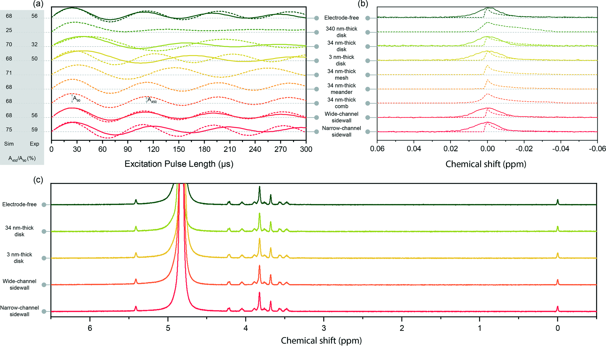 | ||
| Fig. 2 (a) Simulated (dash) and measured (solid) nutation curves for different inserts: electrode-free, planar disk electrodes (340 nm-, 34 nm-, and 3 nm-thickness), structured planar (34 nm thickness) electrodes (mesh, meander, and comb), sidewall electrodes (wide channel (2 mm), narrow channel (1.1 mm)). All nutation signal amplitudes normalised to their 90° intensity. The differences between simulated and measurement signals of the 34 nm-thick planar electrode are discussed in detail in section S4.† (b) Simulated (dash) and measured (solid) 1H NMR spectra of the TSP signal in different configurations. The peak heights are normalised to unity for easier comparison. (c) Measured 1H NMR spectra of the sucrose sample in five different configurations. | ||
From the point of view of B1 performance, a first conclusion offered by the comparative presentation in Table 1 and Fig. 2a was that almost all structures perform in a similar manner: their simulated B1 field homogeneity was at least as good as for the electrode-free case, with the factor A450/A90 between 68% and 75%. The only exception was the 340 nm-thick planar electrode that degraded the B1 field homogeneity to A450/A90 = 25%, i.e., almost one third compared to the electrode-free case. Three structures (34 nm-thick disk, the mesh, and the narrow channel sidewall electrode) showed slightly improved field homogeneity.
The eddy currents induced in the disk metallic structures depleted the B1 field from the centre and concentrated it around the edges of the electrodes. This field distortion increased with the thickness of the metal layer. For a 34 nm-thick layer, this effect led to a flattened field distribution, which enhanced the B1 field homogeneity. The mesh electrode provided multiple closed loops for the eddy current paths, by spreading the field over the entire detection zone, and further enhancing the B1 homogeneity to A450/A90 = 71%. The inter-electrode distance for the narrow channel sidewall configuration was optimised for B1 field homogeneity, reaching a value of A450/A90 = 75%, achieved by both constraining the sample inside the certain region which had the best field homogeneity, and compressing the field inside the sample volume using the sidewall electrodes.
As expected from the analytical expressions given by Chen et al.,23 the thickest planar disk electrode showed the worst performance in terms of mass sensitivity – Srel = 86.4%. For all other structures except for the narrow channel sidewall configuration, the penalty to be paid in comparison with the electrode-free configuration, in terms of mass sensitivity, was <5%. The narrow channel sidewall electrode configuration clearly outperformed all other designs. The sensitivity enhancement for the narrow channel sidewall structure could also be observed through the nutation frequency (Fig. 2a). The slightly higher (1.04×) nutation frequency of the narrow channel sidewall electrode configuration, compared to the electrode-free insert, suggests that the presence of the vertical electrode is constructive and enhances the overall sensitivity.
The planar electrode configurations generate a material interface in the immediate vicinity of the FOV, which degrades the spectral resolution. As discussed in section S4,† this degradation was found to be more severe with increase of the thickness of the metal layer (FWHM = 16.59 ppb for 340 nm and FWHM = 9.05 ppb for 34 nm). However, for a thickness of 3 nm, the spectral resolution returned to a value comparable to the electrode-free configuration, and similar to other structures which had been evaluated. It is interesting to note that all patterned planar electrodes improved the spectral resolution in comparison to a disk electrode with the same thickness, the FWHM value being comparable to the electrode-free case, as shown in Table 1. The spectra collected from the wide and narrow channel sidewall configurations have FWHM of 4.18 ppb and 4.57 ppb, which were similar to the FWHM of the spectrum from the electrode-free insert (4.28 ppb). This was achieved by extending the electrodes along B0 to shift the material interface far from the FOV.
Three additional structures were selected for fabrication and experimental characterisation. These geometries had similar simulated performance and were, importantly, compatible with the electrochemistry experiment designed in section 3.4: the wide channel sidewall electrode structure and, for the ease of fabrication, the 34 nm and 3 nm disk electrode structures. These four structures together with the electrode-free configuration were investigated experimentally and are discussed in the next section.
3.2 Performance analysis of fabricated electrode topologies
The absolute values for the A450/A90 factor, extracted from the nutation curves in Fig. 2a and presented in Table 1, were found to be smaller compared to the simulated values. This is attributed to the fabrication tolerances for the Helmholtz detector, e.g., Helmholtz coil size, slight misalignment of the windings, the distance between two windings, and the effect of the extra tracks which have not been considered in the simulations, as well as the alignment of the insert with respect to the coil.
In contrast with the simulated results, the experiment showed an inferior performance of the structures with planar electrodes in terms of B1 field uniformity when compared to the electrode-free configuration. We attribute this to severe B0 distortions (discussed in section 3.2.3 and S4†) which cannot be fully compensated by shimming. This broadens the linewidth and hence reduces the height of the peak, the effect being more pronounced for higher flip angles due to the additional signal phase deformation.
The two sidewall electrode configurations confirmed experimentally the simulated behaviour. The wide channel sidewall has the same B1 field homogeneity as the electrode-free configuration (A450/A90 = 56%), whereas the narrow channel sidewall electrode exhibits a slightly higher field homogeneity (A450/A90 = 59%).
B 1 maps, collected from MRI experiments, at a flip angle corresponding to 19.2 μW for all five configurations are presented in Fig. 3a. Further B1 profiles at various excitation powers are depicted in Fig. S3.† In order to highlight the field homogeneity, the maps were scaled to unity. Fig. 3b depicts the profile of the B1 field along the x-axis at the middle of the detection zone. For the narrow channel insert, the measurements confirmed that the field homogeneity was enhanced and that a steep drop of the field happened as the sample volume was restricted by the metallic sidewall electrodes.
 | ||
| Fig. 3 (a) Normalised distribution of the B1 field (%) at the sample volume excited with 19.2 μW power for different types of inserts. B1 distributions using different excitation powers can be found in Fig. S3.† (b) Normalised profile of B1 along the x-axis at excitation power of 19.2 μW. (c) B0 field map at the detection zone of the coil. | ||
In order to investigate the B0 distribution more precisely and avoid shimming influence on the results, the B0 maps of different configurations were collected and are plotted in Fig. 2b. The standard deviation calculated from the B0 map was used as a second figure of merit for B0 distribution analysis. These values are presented in Table 1. In all configurations, the detection volume was surrounded by a rim whose voxels were severely distorted due to the partial volume effect (the sample does not fully occupy a voxel) and low B1 field. To calculate the standard deviation of the colour maps, a rim of one pixel was excluded to minimise the noise contribution. At the bottom and top of the detection zone, similar field distortions were observed in all the B0 field maps. This distortion originated from the coil windings.
The B0 pattern at the sensitive zone of the coil showed that the planar 34 nm electrode distorted the static field especially at the top and bottom edges of the electrode, which perfectly aligned the material interface intersections with B0. The ultra-thin electrodes (3 nm thickness) introduced less perturbations; however, the overall pattern appeared similar as expected. These distortions are likely introduced because of the chromium seed layer (see section S3† for further details). Conversely, the narrow channel sidewall electrodes had almost no effect on the overall field pattern, except for the left and right edges where the 1H NMR signal was excluded due to the presence of the electrodes. These results correlated with the measured spectral FWHM results.
3.3 Fabrication challenges and opportunities
According to the measurements and FEM simulations, the sidewall electrodes, with major surfaces parallel to both B0 and B1, and ultra-thin (less that 0.1% of skin-depth) planar electrodes were found to have the best figure-of-merit values. The challenge of introducing conductive structures for in situ electrochemical analyses with high-field NMR is reflected by there being only a few reports available.38–43 Micro-fabrication introduces new opportunities. On one hand, ultra-thin metallic layers, which are NMR transparent, can be achieved by rather standard MEMS techniques. On the other hand, microfabrication enables the construction of precisely oriented high aspect-ratio electrodes, which have a minimum footprint to eliminate any B1 and B0 distortions. Here, we have demonstrated a fabrication technique based on UV-lithography and gold-electroplating to manufacture such electrodes with an aspect ratio (height to width) of ∼3. A further reduction of the width of the electrodes requires more sophisticated lithography techniques, e.g., 2PP, X-ray or e-beam lithography. As an alternative, the distance between the electrodes was optimised in this work to take advantage of the B1 field perturbation, introduced by the electrodes, and enhance the overall field homogeneity and mass sensitivity.Since the narrow channel sidewall electrode configuration proves to be the best compromise in terms of B1 field homogeneity and mass sensitivity, as well as in terms of B0 field distortion, i.e., spectral resolution, this structure was further used for the experiment of NMR in situ monitoring of chitosan electrodeposition.
3.4 In situ electrodeposition of chitosan
Standard electrochemical analyses use three-electrode setups consisting of working, counter, and reference electrodes. Nevertheless, application of a potential between a single pair of electrodes can still be exploited for a variety of uses.Using this electrode configuration, the compatibility of an electrochemical experiment with NMR spectroscopy within a LOC environment was demonstrated using chitosan electrodeposition. This experiment is attractive first because of its relative simplicity, requiring only a voltage applied between 2 electrodes to initiate water hydrolysis, resulting in a local pH gradient as required for chitosan hydrogel deposition. Second, the NMR spectrum of chitosan in solution is significantly different compared to the gel state, and thus the deposition process, as a function of time, can be monitored. Third, chitosan can be chemically modified so that NMR signals from covalently attached molecules can also be monitored as a function of gel formation. Finally, the chitosan hydrogel can be controlled in terms of chemical composition and architecture.16
To perform the in situ experiment, a chitosan (CS) solution was injected into the narrow-channel sidewall insert (1% CS, 50 mM TSP, pH 5.5). Two versions of chitosan were investigated: the native biopolymer, and one chemically modified with polyethyleneglycol (PEG). Prior to applying a current, a 1H NMR spectrum of the solution was measured and NMR calibrations were performed. After the reference spectrum was measured, the current was applied over a working electrode area of 0.42 mm2. The current flowed for the entire experiment, and after intervals of 5 min a new 1H NMR spectrum was acquired. This cycle was repeated so that a total of 5 spectra were measured, the results are summarised in Fig. 4.
 | ||
| Fig. 4 In situ 1H NMR monitoring of chitosan (CS) electrodeposition using the narrow channel sidewall electrode configuration. Results for unmodified CS. (a) CS chemical shift region (pink highlight); (b) TSP signal 0 ppm. Results for CS–PEG: (c) CS–PEG signals (PEG signals in blue highlight); (d) zoom of 2.6–4.0 ppm region to highlight the PEG signals. The time interval between each spectrum was determined by a 5 min delay + 9 min NMR acquisition. In both cases, the water resonance was observed to shift due to a change in pH. The current used to drive electrodeposition was applied during the entire experiment. | ||
The 1H NMR signals from chitosan in solution are clearly visible in the chemical shift range 3 to 4 ppm (pink region in Fig. 4a). As expected, these signals begin broadening as a function of deposition time. The broadening results from constrained molecular motion as would be expected in the hydrogel state. A similar result was observed for chitosan when modified with PEG (Fig. 4c and d). In contrast, the PEG signal (∼3.8 ppm and ∼3.3 ppm, blue region) remained relatively sharp as the hydrogel was formed, suggesting this highly hydrated polymer maintained a degree of molecular motion. This was an interesting result, since bi-functional PEG can be used to attach interesting molecules to chitosan, which would then be potentially decoupled from the deleterious line-broadening effects when deposited as the hydrogel. This feature is currently being explored in continuing work in our group.
4 Conclusions
Introducing metallic electrodes into the NMR detection zone is a challenge to be addressed when performing in situ NMR characterisation of electrochemical processes. The main obstacles to overcome are SNR degradation caused by B1 inhomogeneity and power dissipation in the electrodes, as well as line broadening caused by magnetic susceptibility mismatches. The requirements become even more stringent when integration in a lab-on-a-chip system is required. In order to propose solutions to circumvent these issues, we simulated eight different configurations. Four of those configurations were fabricated and further analysed. The configurations including sidewall electrodes, parallel to both B0 and B1, and the configuration with ultra-thin (less that 0.1% of skin-depth) planar electrodes are found to be the best choices according to the FEM simulations, as well as to the NMR and MRI measurements. Chitosan electrodeposition is presented as an exemplary electrochemistry experiment to be observed by NMR. The chitosan gel state, localised to the electrode surface, is exploited for analyte immobilisation either chemically or physically within the NMR detection volume. In this direction, the quantification of in situ electrodeposition of PEG-modified chitosan was carried out.We conjuncture that the results of this work will be highly relevant for other applications and processes that involve the presence of metallic structures, when these are combined with NMR monitoring. Electrokinetic separation methods, where analytes move through electrolytes under the influence of an applied electric field, are widely used in μ-TAS environments and require the presence of metal electrodes within the device. Dielectrophoresis is another phenomenon extensively used in lab-on-a-chip system to immobilise dielectric particles in non-uniform electric fields. More recently, droplet microfluidics which involves manipulation of droplets of analyte using a planar array of electrodes has been combined with in situ NMR monitoring facing similar challenges.
The methodology presented here can also be extended to other electrode materials compatible with microfabrication and relevant to various electrochemical studies. For example, electrode materials including Ag/AgCl, platinum, and carbon are rather common in 3-electrode electrochemical setups, and indium-tin-oxide (ITO) can be used as transparent electrode, thus enabling direct optical observation at the surface of the electrode where deposition is taking place, or under the electrode in the process chamber.
All similar applications of interest to the lab-on-a-chip community will benefit from the present study, opening new avenues by hyphenating a very chemically specific characterisation method such as NMR with electrochemistry.
Author contributions
The authors report the following individual contributions to this work: conceptualization: HD, NN, JK, NM, VB; data curation: HD, NN, LB; formal analysis: HD, NN, LB; funding acquisition and project administration: NM, VB; investigation: HD, NN, LB; methodology: all; resources: JK, NM, VB; software: HD, LB; supervision: LB, JK, NM, VB; validation: HD, NN, LB, NM, VB; visualisation: HD, NN, LB, VB; writing – original draft: HD, NN, LB, NM, VB; writing – review and editing: HD, NN, JK, NM, VB.Conflicts of interest
The authors declare no conflict of interests.Acknowledgements
HD, NN, NM, and VB acknowledge funding from the Deutsche Forschungsgemeinschaft for the project Bio-PRICE (DFG BA 4275/4-1, DFG MA 6653/1-1), LB acknowledges partial support from the Carl Zeiss Stiftung. LB and JK acknowledge financial support from the European Union [Grant H2020-FETOPEN-1-2016-2017-737043-TISuMR]. NN wishes to thank the University of Malaya and Ministry of Higher Education of Malaysia for the scholarship (SLAB Scheme) and the BioInterfaces International Graduate School (BIF-IGS, www.bif-igs.kit.edu). The authors acknowledge support by the Karlsruhe Nano Micro Facility (KNMF), a Helmholtz Research Infrastructure at Karlsruhe Institute of Technology. Authors also thank Emil Mamleyev and Richard Thelen for the help with SEM and white-light interferometry measurements.References
- V. Badilita, R. C. Meier, N. Spengler, U. Wallrabe, M. Utz and J. G. Korvink, Soft Matter, 2012, 8, 10583–10597 RSC.
- R. M. Fratila, M. V. Gomez, S. Sýkora and A. H. Velders, Nat. Commun., 2014, 5, 3025 CrossRef PubMed.
- E. Montinaro, M. Grisi, M. C. Letizia, L. Pethö, M. A. M. Gijs, R. Guidetti, J. Michler, J. Brugger and G. Boero, PLoS One, 2018, 13, 1–17 CrossRef PubMed.
- O. G. Gruschke, N. Baxan, L. Clad, K. Kratt, D. von Elverfeldt, A. Peter, J. Hennig, V. Badilita, U. Wallrabe and J. G. Korvink, Lab Chip, 2012, 12, 495–502 RSC.
- S. G. van Meerten, K. C. Tijssen, P. J. van Bentum and A. P. Kentgens, J. Magn. Reson., 2018, 286, 60–67 CrossRef CAS.
- A. J. Oosthoek-de Vries, J. Bart, R. M. Tiggelaar, J. W. G. Janssen, P. J. M. van Bentum, H. J. G. E. Gardeniers and A. P. M. Kentgens, Anal. Chem., 2017, 89, 2296–2303 CrossRef CAS.
- W. Hale, G. Rossetto, R. Greenhalgh, G. Finch and M. Utz, Lab Chip, 2018, 18, 3018–3024 RSC.
- M. Sharma and M. Utz, J. Magn. Reson., 2019, 303, 75–81 CrossRef CAS.
- V. Badilita, K. Kratt, N. Baxan, M. Mohmmadzadeh, T. Burger, H. Weber, D. V. Elverfeldt, J. Hennig, J. G. Korvink and U. Wallrabe, Lab Chip, 2010, 10, 1387–1390 RSC.
- R. C. Meier, J. Höfflin, V. Badilita, U. Wallrabe and J. G. Korvink, J. Micromech. Microeng., 2014, 24, 045021 CrossRef.
- N. Spengler, A. Moazenzadeh, R. Meier, V. Badilita, J. Korvink and U. Wallrabe, J. Micromech. Microeng., 2014, 24, 034004 CrossRef.
- N. Spengler, J. Höfflin, A. Moazenzadeh, D. Mager, N. MacKinnon, V. Badilita, U. Wallrabe and J. G. Korvink, PLoS One, 2016, 11, e0146384 CrossRef PubMed.
- L. Bordonali, N. Nordin, E. Fuhrer, N. Mackinnon and J. G. Korvink, Lab Chip, 2019, 19, 503–512 RSC.
- J. Eills, W. Hale, M. Sharma, M. Rossetto, M. H. Levitt and M. Utz, J. Am. Chem. Soc., 2019, 141, 9955–9963 CrossRef CAS PubMed.
- A. Causier, G. Carret, C. Boutin, T. Berthelot and P. Berthault, Lab Chip, 2015, 15, 2049–2054 RSC.
- N. Nordin, L. Bordonali, V. Badilita and N. MacKinnon, Macromol. Biosci., 2019, 19, 1800372 CrossRef.
- J. A. Richards and D. H. Evans, Anal. Chem., 1975, 47, 964–966 CrossRef CAS.
- D. W. Mincey, M. J. Popovich, P. J. Faustino, M. M. Hurst and J. A. Caruso, Anal. Chem., 1990, 62, 1197–1200 CrossRef CAS.
- P. D. Prenzler, R. Bramley, S. R. Downing and G. A. Heath, Electrochem. Commun., 2000, 2, 516–521 CrossRef CAS.
- K. Albert, E.-L. Dreher, H. Straub and A. Rieker, Magn. Reson. Chem., 1987, 25, 919–922 CrossRef CAS.
- V. G. Mairanovsky, L. Y. Yusefovich and T. M. Filippova, J. Magn. Reson., 1983, 54, 19–35 Search PubMed.
- R. D. Webster, Anal. Chem., 2004, 76, 1603–1610 CrossRef CAS PubMed.
- Z.-R. Ni, X.-H. Cui, S.-H. Cao and Z. Chen, AIP Adv., 2017, 7, 085205 CrossRef.
- H. Ryan, A. Smith and M. Utz, Lab Chip, 2014, 14, 1678–1685 RSC.
- I. Swyer, R. Soong, M. D. Dryden, M. Fey, W. E. Maas, A. Simpson and A. R. Wheeler, Lab Chip, 2016, 16, 4424–4435 RSC.
- I. Swyer, S. von der Ecken, B. Wu, A. Jenne, R. Soong, F. Vincent, D. Schmidig, T. Frei, F. Busse, H. J. Stronks, A. J. Simpson and A. R. Wheeler, Lab Chip, 2019, 641–653 RSC.
- B. Wu, S. Ecken, I. Swyer, C. Li, A. Jenne, F. Vincent, D. Schmidig, T. Kuehn, A. Beck, F. Busse, H. Stronks, R. Soong, A. R. Wheeler and A. Simpson, Angew. Chem., Int. Ed., 2019, 58, 15372–15376 CrossRef CAS.
- Y. Cheng, X. Luo, J. Betz, S. Buckhout-White, O. Bekdash, G. F. Payne, W. E. Bentley and G. W. Rubloff, Soft Matter, 2010, 6, 3177–3183 RSC.
- Y. Li, Y. Liu, E. Kim, Y. Song, C.-Y. Tsao, Z. Teng, T. Gao, L. Mei, W. E. Bentley and G. F. Payne, et al. , Carbohydr. Polym., 2018, 195, 505–514 CrossRef CAS PubMed.
- J. Zhuang, S. Lin, L. Dong, K. Cheng and W. Weng, ACS Biomater. Sci. Eng., 2018, 4, 1528–1535 CAS.
- S. Chung, P. Chandra, J. P. Koo and Y.-B. Shim, Biosens. Bioelectron., 2018, 100, 396–403 CrossRef CAS PubMed.
- J. F. Schenck, Med. Phys., 1996, 23, 815–850 CrossRef CAS PubMed.
- M. C. Wapler, J. Leupold, I. Dragonu, D. Von Elverfeld, M. Zaitsev and U. Wallrabe, J. Magn. Reson., 2014, 242, 233–242 CrossRef CAS PubMed.
- G. Milazzo, S. Caroli and R. D. Braun, J. Electrochem. Soc., 1978, 125, 261C CrossRef.
- A. Bard, Standard potentials in aqueous solution, Routledge, 2017 Search PubMed.
- Z. Geng, X. Wang, X. Guo, Z. Zhang, Y. Chen and Y. Wang, J. Mater. Chem. B, 2016, 4, 3331–3338 RSC.
- A. Webb, J. Magn. Reson., 2013, 229, 55–66 CrossRef CAS PubMed.
- P. da Silva, B. Gomes, C. Lobo, L. Júnior, E. Danieli, M. Carmo, B. Blümich and L. Colnago, Microchem. J., 2019, 146, 658–663 CrossRef.
- B. Gomes, P. da Silva, C. Lobo, M. da Santos and L. Colnago, Anal. Chim. Acta, 2017, 983, 91–95 CrossRef CAS PubMed.
- Z. Ni, X. Cui, S. Cao and Z. Chen, AIP Adv., 2017, 7, 085205 CrossRef.
- E. G. Sorte, S. Jilani and Y. J. Tong, Electrocatalysis, 2017, 8, 95–102 CrossRef CAS.
- E. G. Sorte, N. A. Banek, M. J. Wagner, T. M. Alam and Y. J. Tong, ChemElectroChem, 2018, 5, 2336–2340 CrossRef CAS.
- Y. J. Tong, Curr. Opin. Electrochem., 2017, 4, 60–68 CrossRef CAS.
Footnote |
| † Electronic supplementary information (ESI) available. See DOI: 10.1039/d0lc00364f |
| This journal is © The Royal Society of Chemistry 2020 |