DOI:
10.1039/D0LC00235F
(Paper)
Lab Chip, 2020,
20, 2334-2342
Self-aligned 3D microlenses in a chip fabricated with two-photon stereolithography for highly sensitive absorbance measurement†
Received
8th March 2020
, Accepted 18th May 2020
First published on 18th May 2020
Abstract
Absorbance measurement is a widely used method to quantify the concentration of an analyte. The integration of absorbance analysis in microfluidic chips could significantly reduce the sample consumption and contribute to the system miniaturization. However, the sensitivity and limit of detection (LoD) of analysis in microfluidic chips with conventional configuration need improvements due to the limited optical pathway and unregulated light propagation. In this work, a 3D-microlens-incorporating microfluidic chip (3D-MIMC) with a greatly extended detection channel was innovatively fabricated using two-photon stereolithography. The fabrication was optimized with a proposed hierarchical modular printing strategy. Due to the incorporation of 3D microlenses, the light coupling efficiency and the signal-to-noise ratio (SNR) were respectively improved approximately 9 and 4 times. An equivalent optical path length (EOL) of 62.9 mm was achieved in a 3.7 μl detection channel for testing tartrazine samples. As a result, the sensitivity and LoD of the 3D-MIMC assay were correspondingly improved by one order of magnitude, compared with those of the 96-well plate assay. Notably, the 3D-MIMC has the potential to be integrated into a general microanalysis platform for multiple applications.
1. Introduction
Absorbance measurement is a frequently used quantification method for various analysis applications such as immunoassays,1,2 protein quantification,3,4 detection of blood glucose,5 assessment of environmental quality,6–8etc. Compared with absorbance analysis in 1 ml detection cells or 96-well plates, the microfluidic-based assay has attracted lots of attention due to the reduced sample consumption and the miniaturized system. However, the absorbance measurement in conventional microfluidic chips shows marginal advantages in highly sensitive analyses due to the limited optical path length and unregulated light propagation.
The extension of the light pathway proved to be a good way to enhance the sensitivity of absorbance measurement in microfluidic chips,9–11 but the signal-to-noise ratio (SNR) tended to attenuate due to the increased light loss along the pathway. To overcome this problem, it would be effective to adopt optical elements to regulate the light propagation. Lenses, as a fundamental optical element, were frequently incorporated to enhance the coupling efficiency of light in microfluidic chips.12,13 In general, additionally assembled type14,15 and self-aligned type9,16,17 were the two main formats of lens applications. For additionally assembled lenses, necessary position adjustment was commonly required for optimal performance while self-aligned lenses could be used directly. As the representative of assembled lenses, commercial 3D lenses15 or liquid lenses18,19 were adopted for light correction in microfluidic chips. However, additional adjustment or precise control of the liquid interface caused extra complexity and made the system bulky. On the other hand, 2D self-aligned microlenses were incorporated in a microfluidic chip to reduce light loss for absorbance analysis.16 As these self-aligned 2D microlenses were fabricated with the whole microfluidic mold, no additional assembly was required which made it easy to use. Nevertheless, due to the limitation of planar UV lithography, only 2D microlenses have been incorporated and no light can be corrected in the out-of-plane direction.20 In contrast, self-aligned 3D microlenses are more attractive, but to our knowledge, few related studies have been reported so far.
Thermal reflow was a popular method to fabricate 3D microlenses,14,21,22 but it usually could not work straightforwardly for the absorbance application in microfluidic chips due to the mismatch of the microlens axis (out of plane) with the flow path (in plane). In contrast, as a technique of micromachining, two-photon stereolithography is suitable to fabricate arbitrary 3D microstructures with sub-micrometer resolution such as micro motors,23 micro magnetic structures24 and micro scaffolds for cell growth.25,26 It also shows great advantages in manufacturing micro optical structures.27,28 Therefore, it can be a qualified alternative to fabricate 3D microlenses with more freedom of orientation for microfluidic applications. Although a direct fabrication of 3D microlenses in plane using two-photon stereolithography was once reported for photonic integrated circuits,29 to the best of our knowledge, the present study is the first time that 3D microlenses in microfluidic chips were fabricated via mold replication which is valuable due to the added merits such as self-alignment, one-step fabrication and quick replication.
In this study, a 3D-microlens-incorporating microfluidic chip (3D-MIMC) with a long optical path length was fabricated using two-photon stereolithography for highly sensitive absorbance measurement. The main contents are as follows: (1) simulation to optimize microlens dimension and to calculate the theoretical optical performance; (2) proposal of an optimized fabrication strategy and characterization of printed structures; (3) experimental performance of the 3D microlenses; (4) evaluation of the improvements of sensitivity and limit of detection (LoD) based on the test of tartrazine samples; (5) proposal of indexes: equivalent optical path length (EOL) and specific optical path length (SOL) to make an overall assessment of the chip performance for the absorbance measurement.
2. Materials and methods
2.1 Fabrication of the 3D-MIMC
The microfluidic mold was initially designed with the software, AutoCAD 2018. The mold mainly consisted of double fiber grooves, double microlens channels and a detection channel. The geometrical length, width and height of the detection channel were designed as 60 mm, 250 μm and 250 μm, respectively. At the entrance and exit of the detection channel, circular chamfers were designed to prevent the dead zone at the corners. In this mold design, the axis of the 3D microlens was self-aligned with the direction of sample flow. The diameter of the microlens was designed as 250 μm and its thickness was optimized with the Ray Tracing Module in COMSOL. The CAD drawing file was converted into an STL printing file for the fabrication of the microfluidic mold using a two-photon stereolithographic 3D printer (Nanoscribe, Germany).
The main procedures of fabricating the 3D-MIMC are summarized in Fig. 1. Initially, the photoresist (IP-S, Nanoscribe, Germany) was dropped onto the indium tin oxide (ITO) coated glass substrate (Fig. 1a) and selectively polymerized to form the mold using an ultrafast 780 nm laser with 50 mW power. The main part of the mold (Fig. 1b) and critical optical structures including the mold of microlenses and all optical facets of the detection channel and fiber grooves (Fig. 1c) were fabricated separately using different values of printing parameters. The schematics of such hierarchical modular printing are presented in Fig. 1bz and cz, which show the magnified parts of Fig. 1b and c. A 25-fold objective was selected for printing due to its good combination of resolution and working range for printing optical structures without any block stitch. After finishing all printing work, the uncured photoresist was removed by rinsing with the developer (1-methoxy-2-propanol acetate, Sigma, USA) for 18 minutes and IPA (isopropyl alcohol, Sigma, USA) for 2 minutes in sequence (Fig. 1d). Before PDMS casting, the mold was thermally pretreated in an oven at 200 °C for 2 hours for the subsequent efficient separation of the PDMS replica. PDMS and its curing reagent (Sylgard 184, Dow Corning, Midland, USA) were well mixed at the standard ratio of 10![[thin space (1/6-em)]](https://www.rsc.org/images/entities/char_2009.gif) :1 and then were preliminarily degassed in a vacuum desiccator. Afterwards, the homogeneous mixture was cast onto the microfluidic mold and thoroughly degassed to avoid any bubble cavity (Fig. 1e). After polymerization at 70 °C for 4 hours, the cured PDMS was carefully peeled off from the mold and then was punched to form holes (Fig. 1f). Finally, the PDMS layer was bound onto the glass substrate after the plasma treatment (Fig. 1g).
:1 and then were preliminarily degassed in a vacuum desiccator. Afterwards, the homogeneous mixture was cast onto the microfluidic mold and thoroughly degassed to avoid any bubble cavity (Fig. 1e). After polymerization at 70 °C for 4 hours, the cured PDMS was carefully peeled off from the mold and then was punched to form holes (Fig. 1f). Finally, the PDMS layer was bound onto the glass substrate after the plasma treatment (Fig. 1g).
 |
| | Fig. 1 The main procedures of manufacturing the 3D-MIMC. (a) IP-S photoresist is dropped onto the ITO glass substrate. (b) The primary part is printed on the substrate. (c) The microlens mold and all optical facets are printed separately. (d) Removing the uncured photoresist. (e) PDMS casting to replicate the structures. (f) PDMS curing, separation from the mold and hole punching. (g) Substrate binding to form the chip. (bz) and (cz) The zoomed-in images of (b) and (c) to show the separate printing for the microlens mold and optical facets. For a full view of the structure with clear details, the omitted part of the detection channel was marked with a white wavy line. | |
2.2 System configuration
A neutral white LED (MNWHD2, Thorlabs, USA) mounted on a cooling sink was selected as the light source. The light was guided from its source to the detection channel via the bare multimode input-fiber (Thorlabs, FG105UCA, coat/core diameter–250/105 μm, and numerical aperture–0.22 in air). The fiber was confined in a chip groove. The light emitted from the input-fiber was converged by the input-microlens before entering the detection channel. When transmitting in the detection channel, part of the light was absorbed by sample molecules. Afterwards, the light leaving the detection channel was converged again by the output-microlens and then was guided by the output-fiber to the spectrometer (ULS2048LTEC, Avantes, Netherlands). The schematic of the system configuration is shown in Fig. 2.
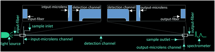 |
| | Fig. 2 Schematic of the system configuration. The end facets of the detection channel and fibers as well as the microlens channels were magnified to present clear details. | |
2.3 Simulation methods
As the ray emitter (the core of the input-fiber end) was comparable to the microlens in dimension, it could not be simplified as a single point source. In this study, the ray emitter was assumed as a collection of multiple point sources. Considering the symmetry of the ray emitter and 3D spherical microlens in the Y–Z plane (Fig. 3a), an integration on the whole emitter plane (depicted as the bold cyan arrow in Fig. 3b) was conducted to calculate the overall optical performance in the 3D-MIMC. This integration was based on representative sources distributed along the emitter radius (marked as cyan dots in Fig. 3b). More details of the simulation settings are provided in the ESI (Fig. S1 and S2†).
 |
| | Fig. 3 (a) Symmetry of the ray emitter and 3D microlens in the Y–Z plane. (b) Representative ray sources (cyan dots) distributed along the emitter radius and an integration on the emitter plane (cyan arrow). | |
2.4 Analytical methods
When the light propagates through the detection channel filled with solution samples, the light intensity attenuates due to the absorption caused by sample molecules. The magnitude of such an attenuation is proportional to both the analyte concentration and the length of the optical pathway, which is described by the Beer–Lambert law30 and expressed as eqn (1). This equation is the principle for quantitative absorbance analysis.| |  | (1) |
where A is the absorbance value, I is the intensity of the light transmitted through the samples, I0 is the intensity of the light transmitted through the reference sample, ε is the molar attenuation coefficient, c is the concentration of the analyte, and l is the optical length.
As a synthetic organic food dye, the detection of tartrazine has attracted lots of attention in the fields of food analysis and food safety.31 Additionally, tartrazine was used as a test sample for absorption analysis.32 Therefore, in this work, tartrazine (T0388-100, Sigma, USA) was adopted as the test sample to evaluate the performance of the 3D-MIMC. Tartrazine samples were prepared at various concentrations ranging from 6.25 to 500 ppb in Millipore water. Glucose powder (G8270-100, Sigma, USA) was dissolved in Millipore water to prepare a 50% (w/w) glucose solution for checking the performance of the microlenses. Test samples in the microfluidic chip were loaded by a peristaltic pump (REGLO Digital MS-4/6, ISMATEC, Germany) at a constant flow rate of 8 μl min−1. The transmitted light from the detection channel was guided by the output-fiber and recorded by the spectrometer. The light intensity at 428 nm, which was the peak wavelength of absorbance for tartrazine samples, was extracted and the absorbance value was calculated according to eqn (1). The repeatability of microlens performance and absorbance measurement among three microfluidic chips was checked. Besides the microfluidic-based assay, the absorbance of all the samples was also measured in a 96-well plate using an absorbance reader (Infinite 200 PRO, Tecan, Switzerland) for the comparative study.
3. Results and discussion
3.1 Simulation for optimizing microlens dimension
To avoid an arbitrary design, the Ray Tracing Module in COMSOL was used to investigate the theoretical optical performance with different microlens configurations. The optical performance was quantified according to the total probability of rays received by the detector (the core of the output-fiber end). This probability in the microfluidic chip without microlenses (MC) was used to normalize that in the microfluidic chip with 2D microlenses (2D-MIMC) and that in 3D-MIMC. The normalized result was expressed as the enhancement of light coupling efficiency. The ray emitter and detector were respectively located at the back focus positions of the input-microlens and output-microlens. The focus distance was calculated according to eqn (2).14 The relevant schematic plot of dimension illustration is shown in Fig. 4a. The qualitative comparison of ray trajectories in Fig. S3† suggested that the 3D microlens could obviously reduce the divergence of light emitted from the optical fiber while the 2D microlens could only partly correct the light propagation. The quantitative simulation results in Fig. 4b indicated that the 3D microlenses could theoretically enhance the light coupling efficiency by up to 30 times and they remarkably outperformed the 2D microlenses. To optimize the design of the 3D microlenses, the influence of microlens thickness was also investigated. As shown in Fig. 4b, the enhancement of light coupling efficiency had minor variations between 9.6 and 36 μm while it obviously deteriorated with the increase of microlens thickness from 36 to 53.4 μm. The best optical performance was achieved at the microlens thickness of 25 μm. Thus, a lens thickness of 25 μm was adopted as the optimal microlens dimension for the subsequent fabrication.| |  | (2) |
where fb is the back focal length of the microlens, n1 is the refractive index (RI) of the microlens material (in this work, the microlens material was PDMS (RI = 1.41)), n2 is the RI of the medium between the microlens and optical fiber (in this work, the medium was also PDMS), R is the curvature radius of the microlens and h is the thickness of the microlens.
 |
| | Fig. 4 Simulation for optimizing the microlens dimension. (a) The illustrative dimension schematic of the 3D microlens and its back focus position. (b) The comparison of theoretical performance of 2D microlenses (solid black dots) and 3D microlenses (void cyan triangles). In the simulation, the width and height of the 2D microlens were both set to 250 μm, which was identical to the diameter of the 3D microlens. Other configurations were the same for both 2D-MIMC and 3D-MIMC. | |
3.2 Chip fabrication using two-photon stereolithography
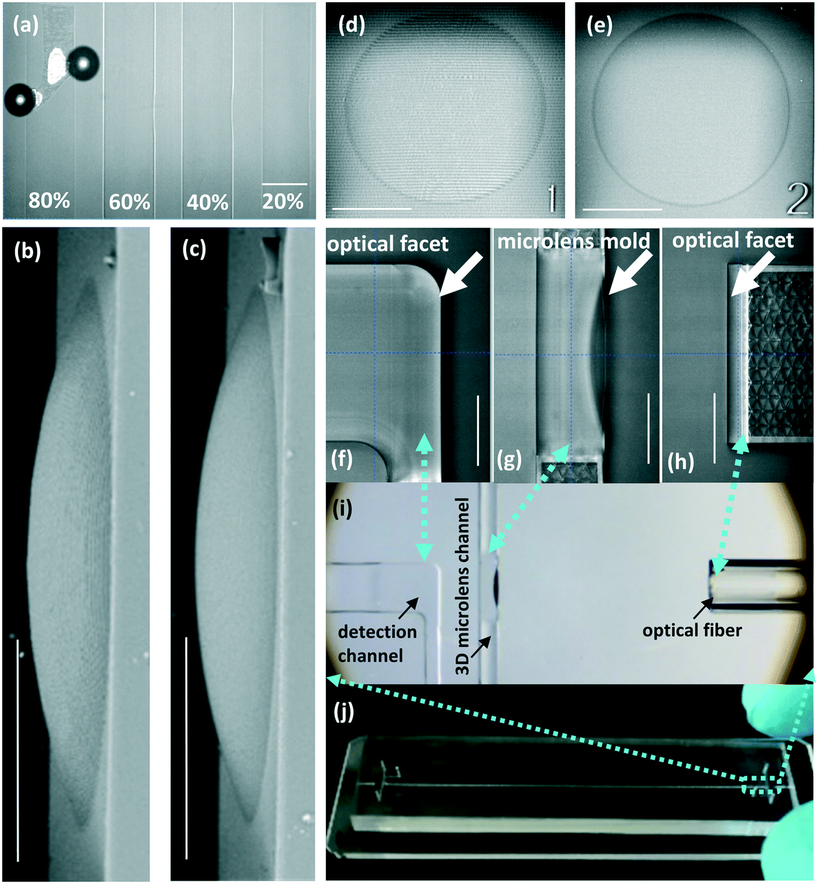
In this study, a strategy of hierarchical modular printing was proposed to strike a balance between the acceptable total printing time and high quality of critical optical structures. Considering the bulk printing volume and the absence of key optical structures, a shell-scaffold-printing method was adopted to fabricate the primary part of the chip mold. Correspondingly, the values of parameters including the slicing distance (SD), hatching distance (HD) and laser dose (LD) were respectively set to 1 μm, 0.5 μm and 70%. As for the parts of the microlenses and optical facets, a solid-printing method was adopted. Before the solid printing, levels of SD, HD and LD were additionally tested for improving the quality of the optical structures. The effects of LD within 20% to 80% are compared in Fig. 5a. It was found that when the LD was set as high as 80%, the emergence of bubbles caused a low printing quality. In contrast, with the LD as weak as 20%, the blur profile of the structure suggested an incomplete polymerization of the photoresist. Therefore, 40–60% should be the appropriate range of the LD. The effects of the SD and HD on the structure quality were comparatively shown in the SEM images of the 3D microlenses (side view: Fig. 5b and c, top view: Fig. 5d and e). As a consequence of the coarse printing configuration, ridges could be clearly observed on the microlens surface in Fig. 5b and d. In contrast, due to the small value of SD (0.2 μm) and HD (0.2 μm), the microlens surface in Fig. 5c and e proved to be smoother than that shown in Fig. 5b and d. Based on the results of the printing parameter test, 40% LD, 0.2 μm SD and 0.2 μm HD were selected in this work for printing the microlens mold and all optical facets.
 |
| | Fig. 5 Fabrication parameters of the 3D-MIMC. (a) Effects of laser dose (LD) for printing the microlens and all optical facets. SEM images of microlenses with different levels of SD and HD: (b) side view, SD: 1.0 μm, HD: 0.5 μm; (c) side view, SD: 0.2 μm, HD: 0.2 μm; (d) top view, SD: 1.0 μm, HD: 0.5 μm; (e) top view, SD: 0.2 μm, HD: 0.2 μm. Key optical structures were successfully fabricated using a hierarchical modular printing strategy: (f) Optical facet of the detection channel; (g) Microlens mold; (h) Optical facet of the fiber groove. (i) Optical fiber, microlens and detection channel self-aligned in the chip. (j) An actual overview of the 3D-MIMC. The correspondence of (f)–(h) to the entire 3D-MIMC was marked with cyan dash arrows in the images. Scale bar in images: 100 μm. | |
Based on the hierarchical modular printing strategy aforementioned, the microlens mold and all optical facets were successfully fabricated (Fig. 5f–h). To the best of our knowledge, it was the first time that 3D microlenses (in plane) in microfluidic chips were fabricated via mold replication. Although the microlens mold was a concave 3D structure, the PDMS replica was successfully peeled off due to its elasticity. Particularly, as the microlens mold was fabricated with the whole chip mold, our approach eliminated the need for additional assembly or alignment and thus made the use very convenient. Corresponding to the mold structures, Fig. 5i shows their replica in the PDMS chip after bonding with the glass slide and inserting the optical fiber. In this chip, the detection channel, the microlenses and the optical fibers were mutually self-aligned. An overview of the actual 3D-MIMC is presented in Fig. 5j.
3.3 Performance of 3D microlenses
In this study, 3D microlenses were incorporated into channels as an optofluidic design. With this configuration, it is easy to change the refractive index (RI) of channel fillings to achieve an optical adjustment as required.18,33 Therefore, the performance of microlenses could be characterized in situ by replacing the channel filling. For instance, the RI value of 50% (w/w) glucose solution was 1.41,34 which was equivalent to that of PDMS. Thus, this solution was used to eliminate the converging effect of the microlenses. Fig. 6a describes the variation of the light intensity with the change of medium in the microlens channels from air to glucose solution while the detection channel was filled with Millipore water. Initially, both the input-microlens and output-microlens channels were filled with air (RI = 1). The microlenses were in effect due to the significant difference in RI between air and PDMS. Therefore, the divergence of light was corrected. Afterwards, a 50% (w/w) glucose solution was successively pumped into the input-microlens and output-microlens channels and then no difference in RI existed anymore. As a result of this replacement, two correspondingly successive drops of the light intensity are observed in Fig. 6a. The light coupling efficiency in total was reduced by approximately 9 times in which approximately 4 times of the reduction was attributed to the elimination of the input-microlens converging effect. The effectiveness of the input-microlens, which was defined as the ratio of the experimental to theoretical enhancement of light coupling efficiency, was 70% on average while the effectiveness of the output-microlens was approximately 42% (Fig. 6b). The difference between the theoretical and experimental results might be caused by the following factors. First, for simplifying the calculation in simulation, no secondary reflection at the walls of the detection channel was considered which might lead to bias of the computed probability of rays recorded by the detector. Second, although the fabrication of the microlens and critical optical facets was optimized, due to the resolution limitation of stereolithography, these structures could not be perfectly smooth. Consequently, it could cause light loss by scattering. Fig. 6c reflects the noise level of the baseline test within 600 s in the MC and the 3D-MIMC. Despite the increased noise in the 3D-MIMC, due to the strong enhancement of light coupling efficiency, the SNR (conventionally defined as the mean of signal intensity divided by the standard deviation of the noise level) was approximately improved 4 times (Fig. 6d), which enabled the detection of a lower concentration of the analyte. The acceptable range of error bars in Fig. 6b and d suggested a good repeatability of the microlens performance among the chips.
 |
| | Fig. 6 Experimental performance of 3D microlenses. (a) Change of light intensity when successively injecting 50% (w/w) glucose solution into the microlens channels. (b) Comparison of the experimental and theoretical enhancement of light coupling efficiency. Tin, Tout – theoretical performance of input-microlens, output-microlens; Ein, Eout – experimental performance of input-microlens, output-microlens. (c) Noise level of the baseline test within 600 s in the MC (black line) and 3D-MIMC (cyan line). (d) SNR comparison. All data of light intensity in (a) and noise in (c) were uniformly normalized by the average light intensity recorded by the spectrometer in the 3D-MIMC for the baseline test. The error bars in (b) and (d) corresponded to the standard deviation of the measured microlens performance among the three chips (n = 6). | |
3.4 Improvement of sensitivity and limit of detection
Fig. 7a and b, respectively, show the real-time results of the tartrazine test based on the MC and 3D-MIMC. All data of light intensity were converted to the absorbance data according to eqn (1). After each injection of samples, Millipore water was loaded to rinse the detection channel. The insets in Fig. 7a and b are the magnified plots of signal responses after loading 6.25 ppb tartrazine solution. It was found that this low concentration of the sample could not cause a distinguishable signal response in the MC. Comparatively, due to the enhanced SNR in the 3D-MIMC, a clear change of light intensity was recognized. All the samples were also measured in parallel using the 96-well based assay for a comparative study. The data from the microfluidic chip based assays and the 96-well plate based assay were extracted for regression analysis. As summarized in Fig. 7c, significant linear relationships (R2 > 0.99) were established between the tartrazine concentration and absorbance for all three assays. Prominently, the slope values of the curves based on the MC and 3D-MIMC were respectively as high as 324.8 × 10⁻⁶ (ppb)−1 and 326.5 × 10⁻⁶ (ppb)−1 while the value of the 96-well plate based curve was only 32.2 × 10⁻⁶ (ppb)−1. It indicated that due to the elongated optical pathway in the microfluidic chips, the sensitivity of the tartrazine test was enhanced approximately by one order of magnitude, compared with that based on the 96-well plate. Although the detection sensitivity in the MC and 3D-MIMC was almost the same, a remarkable disparity of LoD existed. To derive the value of LoD, the signal threshold of absorbance was conventionally defined as three times the noise level of absorbance.8 The absorbance noise of all assays was assumed as the standard deviation of the absorbance for tests of reference samples. With the value of the absorbance threshold, the LoD for the tartrazine test could be derived from the regression equations shown in Fig. 7c. As summarized in Fig. 7, the average LoD based on the 3D-MIMC assay was calculated as 3 ppb, which was significantly improved, compared with those based on the 96-well plate (26 ppb) and MC (12 ppb) assays.
 |
| | Fig. 7 Real time results of the tartrazine test in the MC (a) and 3D-MIMC (b). The insets show the corresponding magnified plots of signal response after injecting samples (6.25 ppb). The black dash lines in the insets are the lines of the absorbance threshold. The presented regression results (c) and LoD comparison (d) were based on 96-well plate, MC and 3D-MIMC assays. The error bars in Fig. 7c and d respectively corresponded to the standard deviation of the measured absorbance values and LoD in the tests of tartrazine samples (n = 6). | |
3.5 Equivalent/specific optical path length
Microfluidic chips for absorbance analysis have attracted lots of attention. It is of importance to quantitatively assess the overall performance in terms of sensitivity and sample consumption for comparing data with published results. The optical length is a decisive factor for the sensitivity of absorbance measurement. Although the value of optical length can be derived according to eqn (1), the molar attenuation coefficient of various actual samples is usually not easy to acquire. In some papers, the optical length was simplified as the geometrical length of the detection cell along the direction of light propagation. However, the adoption of the geometrical optical length (GOL) might cause biases since light is inherently divergent.20 To address this problem, the equivalent optical path length (EOL) was proposed in this study. For calculating the EOL, the 96-well plate with a 200 μl sample volume was adopted as the reference detection cell. The reference optical length of this cell was determined to be 6.2 mm according to the sample volume and the size of the well (internal diameter–6.40 mm). Based on the reference value, the EOL for the sample test in microfluidic chips could be calculated according to eqn (3). The EOL can also be used as an inspection indicator of stray light. The stray light is a great concern in optimizing optical systems,20,33,35,36 as it can increase the noise level and reduce the sensitivity of optical analysis. Normally, the EOL value should not be smaller than the GOL value due to light divergence. Otherwise, it can imply that the optical detector has recorded stray light. Besides the EOL, the specific optical length (SOL) was proposed as well to characterize the effectiveness of sample consumption. Subscripts G and E were respectively added to the SOL to differentiate the values derived from GOL and EOL according to eqn (4) and (5). As EOL and SOLE were not directly available for detection cells in the cited papers, the comparative results of GOL and SOLG are summarized in Table 1. The commercial detection cells proved to be the least competitive in terms of GOL and SOLG. As for microfluidic chips reported in the literature, the GOL was generally less than 25 mm20 and the SOLG was approximately 10 mm μl−1. Although a high value of SOLG was achieved for the absorbance detection of droplets,15 the GOL was very small. Compared with the detection cells on the market and those reported in the literature, as the GOL and SOLG of the 3D-MIMC in this study were 60 mm and 16.2 mm μl−1, it had obvious advantages in both sample consumption and analysis sensitivity. The EOL and SOLE of the 3D-MIMC are also included in Table 1. Their values were approximately 5% higher than those of the GOL and SOLG. It indicated that little stray light was recorded in the 3D-MIMC. As a long EOL (62.9 mm for tartrazine test) was achieved in the tiny detection channel (3.7 μl), it enabled the sensitive absorbance analysis to use very small volume of samples.| | 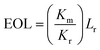 | (3) |
where Km and Kr are the slope values of regression curves respectively based on the microfluidic assay and reference assay, Lr is the geometrical optical length of the reference detection chamber, and Vm is the volume of the detection chamber in the microfluidic chip.
Table 1 Comparison with results from the literature and commercial cells
| Literature |
GOL (mm) |
SOLG (mm μl−1) |
Sample |
| 1 ml standard cell |
10 |
0.010 |
— |
| 200 μl 96-well plate |
6.2 |
0.031 |
— |
| (Yang et al. 2017)15 |
0.8 |
879 |
Droplet of fluorescein buffer |
| (Rodríguez-Ruiz et al. 2015)16 |
10 |
10 |
Protein samples |
| (Sieben et al. 2010)8 |
25 |
11.1 |
Aquatic nitrite |
| This work |
60 |
16.2 |
Tartrazine solution |
| EOL (mm) |
SOLE (mm μl−1) |
| This work |
62.9 |
17.0 |
Tartrazine solution |
Conclusions
In this paper, a 3D-MIMC was innovatively manufactured using two-photon stereolithography for a highly sensitive absorbance measurement. The 3D-MIMC fabrication was optimized using the proposed hierarchical modular printing strategy. As a result of the configuration of the 3D microlenses, the light coupling efficiency increased approximately 9 times. This enhancement enabled the extension of the optical pathway as well as improved the SNR. Beneficially, the tartrazine analysis was greatly improved in both sensitivity and LoD. To quantitatively assess the overall performance of this chip, two indexes, EOL and SOL, were proposed based on analysis sensitivity and sample consumption. It was found that an EOL of 62.9 mm was achieved for tartrazine tests in a 3.7 μl detection channel. For future work, this microfluidic chip has the potential to be coupled with micro reactors to function as an integrated microanalysis platform.
Conflicts of interest
The authors declare no conflicts of interest.
Acknowledgements
We thank Prof. Dr. Andrew de Mello of the Institute of Chemical and Bioengineering, ETH Zürich for the permission to use the cleanroom of his group.
References
- N. Párraga-Niño, S. Quero, A. Ventós-Alfonso, N. Uria, O. Castillo-Fernandez, J. J. Ezenarro, F.-X. Muñoz, M. Garcia-Nuñez and M. Sabrià, Talanta, 2018, 189, 324–331 CrossRef PubMed.
- Q. Sun, G. Zhao and W. Dou, Anal. Methods, 2015, 7, 8647–8654 RSC.
- T. Song, S. Wang, Y. Zhang, J. Song, F. Liu, P. Fu, M. Shiraiwa, Z. Xie, D. Yue and L. Zhong, Environ. Sci. Technol., 2017, 51, 6773–6781 CrossRef CAS PubMed.
- C. V. Sapan and R. L. Lundblad, Proteomics: Clin. Appl., 2015, 9, 268–276 CAS.
- P. Zhang, D. Sun, A. Cho, S. Weon, S. Lee, J. Lee, J. W. Han, D.-P. Kim and W. Choi, Nat. Commun., 2019, 10, 1–14 CrossRef PubMed.
- Y. Date, S. Terakado, K. Sasaki, A. Aota, N. Matsumoto, H. Shiku, K. Ino, Y. Watanabe, T. Matsue and N. Ohmura, Biosens. Bioelectron., 2012, 33, 106–112 CrossRef CAS PubMed.
- A. D. Beaton, C. L. Cardwell, R. S. Thomas, V. J. Sieben, F.-E. Legiret, E. M. Waugh, P. J. Statham, M. C. Mowlem and H. Morgan, Environ. Sci. Technol., 2012, 46, 9548–9556 CrossRef CAS.
- V. J. Sieben, C. F. Floquet, I. R. Ogilvie, M. C. Mowlem and H. Morgan, Anal. Methods, 2010, 2, 484–491 RSC.
- J. Vila-Planas, E. Fernández-Rosas, B. Ibarlucea, S. Demming, C. Nogués, J. A. Plaza, C. Domínguez, S. Büttgenbach and A. Llobera, Nat. Protoc., 2011, 6, 1642–1655 CrossRef CAS.
- A. Gáspár, I. Bácsi, E. F. Garcia, M. Braun and F. A. Gomez, Anal. Bioanal. Chem., 2009, 395, 473–478 CrossRef PubMed.
- J.-Z. Pan, B. Yao and Q. Fang, Anal. Chem., 2010, 82, 3394–3398 CrossRef CAS PubMed.
- H. Yang and M. A. Gijs, Chem. Soc. Rev., 2018, 47, 1391–1458 RSC.
- D.-X. Lu, Y.-L. Zhang, D.-D. Han, H. Wang, H. Xia, Q.-D. Chen, H. Ding and H.-B. Sun, J. Mater. Chem. C, 2015, 3, 1751–1756 RSC.
- G. Holzner, Y. Du, X. Cao, J. Choo, A. J. de Mello and S. Stavrakis, Lab Chip, 2018, 18, 3631–3637 RSC.
- T. Yang, S. Stavrakis and A. de Mello, Anal. Chem., 2017, 89, 12880–12887 CrossRef CAS PubMed.
- I. Rodríguez-Ruiz, M. Conejero-Muriel, T. N. Ackermann, J. A. Gavira and A. Llobera, Lab Chip, 2015, 15, 1133–1139 RSC.
- J. Seo and L. P. Lee, Sens. Actuators, B, 2004, 99, 615–622 CrossRef CAS.
- H. Zhao, Y. Yang, L. Chin, H. Chen, W. Zhu, J. Zhang, P. Yap, B. Liedberg, K. Wang and G. Wang, Lab Chip, 2016, 16, 1617–1624 RSC.
- X. Mao, J. R. Waldeisen, B. K. Juluri and T. J. Huang, Lab Chip, 2007, 7, 1303–1308 RSC.
- I. Rodríguez-Ruiz, T. N. Ackermann, X. Muñoz-Berbel and A. Llobera, Anal. Chem., 2016, 88, 6630–6637 CrossRef PubMed.
- J. Qiu, M. Li, H. Ye, J. Zhu and C. Ji, Sens. Actuators, A, 2018, 279, 17–26 CrossRef CAS.
- J. Lim, P. Gruner, M. Konrad and J.-C. Baret, Lab Chip, 2013, 13, 1472–1475 RSC.
- G. Vizsnyiczai, G. Frangipane, C. Maggi, F. Saglimbeni, S. Bianchi and R. Di Leonardo, Nat. Commun., 2017, 8, 15974 CrossRef CAS PubMed.
- G. Williams, M. Hunt, B. Boehm, A. May, M. Taverne, D. Ho, S. Giblin, D. Read, J. Rarity and R. Allenspach, Nano Res., 2018, 11, 845–854 CrossRef.
- P. Tayalia, C. R. Mendonca, T. Baldacchini, D. J. Mooney and E. Mazur, Adv. Mater., 2008, 20, 4494–4498 CrossRef CAS.
- J. Lölsberg, A. Cinar, D. Felder, G. Linz, S. Djeljadini and M. Wessling, Small, 2019, 15, 1901356 CrossRef PubMed.
- S. Juodkazis, Nat. Photonics, 2016, 10, 499–501 CrossRef CAS.
- T. Gissibl, S. Thiele, A. Herkommer and H. Giessen, Nat. Photonics, 2016, 10, 554–560 CrossRef CAS.
- R. Thomas, J. Li, S. Ladak, D. Barrow and P. Smowton, Opt. Express, 2018, 26, 13436–13442 CrossRef CAS PubMed.
- D. Swinehart, J. Chem. Educ., 1962, 39, 333 CrossRef CAS.
- R. Sahraei, A. Farmany and S. Mortazavi, Food Chem., 2013, 138, 1239–1242 CrossRef CAS PubMed.
- H. Waechter, K. Bescherer, C. J. Dürr, R. D. Oleschuk and H.-P. Loock, Anal. Chem., 2009, 81, 9048–9054 CrossRef CAS PubMed.
- J. Dietvorst, J. Goyvaerts, T. N. Ackermann, E. Alvarez, X. Muñoz-Berbel and A. Llobera, Lab Chip, 2019, 19, 2081–2088 RSC.
- C.-Y. Tan and Y.-X. Huang, J. Chem. Eng. Data, 2015, 60, 2827–2833 CrossRef CAS.
- R. R. Svejdal, E. R. Dickinson, D. Sticker, J. R. P. Kutter and K. D. Rand, Anal. Chem., 2018, 91, 1309–1317 CrossRef PubMed.
- R. Lanfranco, J. Saez, E. Di Nicolò, F. Benito-Lopez and M. Buscaglia, Sens. Actuators, B, 2018, 257, 924–930 CrossRef CAS.
Footnote |
| † Electronic supplementary information (ESI) available. See DOI: 10.1039/d0lc00235f |
|
| This journal is © The Royal Society of Chemistry 2020 |
Click here to see how this site uses Cookies. View our privacy policy here. 
 Open Access Article
 This Open Access Article is licensed under a Creative Commons Attribution-Non Commercial 3.0 Unported Licence
 *ab
*ab