
Depth profiling by pulsed glow discharge time-of-flight mass spectrometry with a combined hollow cathode cell†
Anna
Gubal
 a,
Victoria
Chuchina
a,
Yegor
Lyalkin
a,
Vladimir
Mikhailovskii
a,
Viktor
Yakobson
b,
Nikolay
Solovyev
*ac and
Alexander
Ganeev
ad
a,
Victoria
Chuchina
a,
Yegor
Lyalkin
a,
Vladimir
Mikhailovskii
a,
Viktor
Yakobson
b,
Nikolay
Solovyev
*ac and
Alexander
Ganeev
ad
aSt. Petersburg State University, Institute of Chemistry, Universitetskaya nab. 7/9, 199034 St. Petersburg, Russia. E-mail: n.solovyev@spbu.ru
bJoint Stock Company “Research and Production Corporation S.I. Vavilova”, ul. Babushkina 36-1, 192171 St. Petersburg, Russia
cInstitute of Technology Sligo, Ash Lane, Sligo, F91 YW50, Ireland. E-mail: solovyev.nikolay@itsligo.ie
dInstitute of Toxicology of Federal Medico-Biological Agency, ul. Bekhtereva 1, 192019 St. Petersburg, Russia
First published on 19th June 2020
Abstract
A combined hollow cathode microsecond direct current pulsed glow discharge time-of-flight mass spectrometry (CHC μs-DC-PGD TOFMS) system has proved its efficiency for quantification; however, it has not been properly tested for the purpose of depth analysis until now, to the best of the authors' knowledge. The aim of the current study was to investigate the capabilities of this glow discharge source type for depth profiling. Special attention was paid to the alteration of depth resolution during the sputtering and the effect of discharge parameters on the crater shape in different types of solid samples. Both dielectric and conductive samples were tested, including: a Ni film on silicon, a Si film on borosilicate glass, and IR-reflective dielectric multilayer (mirror) coatings. Crater shapes were investigated after combined hollow cathode cell sputtering to ensure reliable profiling. For dielectric materials, including multilayer coatings, the deposition of a thin conducting layer (Ag or Ta) on the sample surface was demonstrated to result in reliable sputtering with adequate depth resolution of the profiling. This preliminary sample coating provided both the formation of required surface conductivity and reduction of the negative effect of atmospheric gases and water surface contamination at the beginning of sample sputtering. A silicon-coated borosilicate glass specimen was tested for potential quantitative profiling, showing promising results. The CHC μs-DC-PGD TOFMS system used was capable of analyzing the layers of varied thickness in the range from tens of nanometers to several micrometers. The depth resolution was 5 nm and 25 nm for conducting and dielectric layers, respectively.
1. Introduction
For different materials science and engineering tasks, there is a high demand for direct and sensitive quantification and depth profiling of a wide range of elements in varied solids. Glow discharge (GD) optical emission spectrometry (GDOES) and mass spectrometry (GDMS) are effective tools fit-for-purpose for such analytical challenges, providing superior analytical figures of merit.1–12 The primary advantage of these techniques is rapid depth profiling for both ultrathin13–16 and relatively thick films and coatings17–19 with high layer-by-layer resolution of several nanometers. Recently, Lobo et al.2 and Nelis and Palossi12 published excellent reviews summarizing the capabilities of glow discharge techniques. Additionally, there are several studies published comparing GDMS and GDOES with other techniques including Rutherford backscattering spectrometry (RBS), Auger electron spectroscopy (AES), X-ray photoelectron spectrometry (XPS), and secondary ion mass spectrometry (SIMS).3,9,16,20,21Notably, GDOES is mainly used in depth analysis.10,11 Starting from the pioneering studies of Green and Whelan22 in the early 1970s, GDOES has become a powerful tool of layer-by-layer analysis. Nevertheless, with gradual progress in material sciences, lower limits of detection (LoDs) are required for reliable profiling of dopants and impurities in thin films, e.g., in photovoltaics. Higher requirements for analysis sensitivity stimulated the development of GDMS as a replacement for GDOES for element depth profiling.6,7 Radiofrequency (RF) and pulsed RF glow discharge (RF-PGD) are the most effective GD sources for the purpose, especially when combined with a time-of-flight mass spectrometer (TOFMS).8,9,23–26 In particular, RF-PGD-TOFMS is capable of layer-by-layer analysis of dielectric samples, which are highly problematic for direct current (DC) discharge GDMS17,27,28 with a secondary cathode.29
Different types of pulsed GD sources – RF-PGD and microsecond DC μs-DC PGD – provide additional analytical possibilities for varied sample types, enabling the use of different temporal ranges of pulsed plasma and its afterglow.30,31 This flexibility opens wider possibilities for fine optimization of discharge parameters in respect of sensitivity and depth resolution (currently achievable values are ca. 1–3 nm).3,9,14,16,32,33 The use of PGD sources increases ionization efficiency with simultaneous alleviation of heat burden on the discharge cell and the sample under study. This is important for the analysis of thermally unstable materials including their depth analysis.34 For more details on this source type, the reader is referred to the review by Pisonero et al.9
The depth resolution in GDMS is primarily determined by the sputtering crater shape.32,35 In turn, the crater shape is dependent on discharge parameters, such as pressure, discharge current, discharge pulse duration and frequency (for PGD sources). Thus, the optimization of the parameters of the layer-by-layer analysis is aimed, first of all, for obtaining a flat-bottom rectangular crater with sufficient signal intensities. In addition to the crater shape profiling after the sputtering, the depth resolution can be evaluated by the sharpness of the interface between the layers, which is often used as an alternative to crater profilometry.32,35
The crater shape and depth resolution are also affected by the geometry of the discharge. In the majority of cases, for the layer-by-layer analysis, a Grimm cell is used. This cell type provides homogeneous distribution of electric potential at the sample surface and homogeneous sputtering with a flat-bottom crater.1 Another GD-source type, hollow cathode (HC), is virtually not used for depth profiling. To the best of our knowledge, the first application of HC for depth profiling was attempted by Djulgerova et al.36 A liquid nitrogen cooled deep hollow cathode made of Al was used. A sample was inserted inside the HC at its bottom part. However, the crater shape or depth resolution was not investigated. So the possibilities of the type of cell for depth profiling of various coated or especially multilayer samples remain unclear.
The combined hollow cathode (CHC) consists of a flat sample and auxiliary short cylindrical metal cathode. It is a more convenient variant of HC to serve as a GD-source. It is simple in handling, while positioning the sample, and has almost no limitations on the sample shape except the flat surface. The CHC applied in μs-DC PGD does not require cooling and is operable with non-conducting materials. The efficiency of sputtering, contrary to the RF-PGD, does not depend on the sample thickness.37 The use of dynamic effect in μs-DC-PGD (under short delays of repelling pulse relative to the discharge pulse) allows for effective ionization of high ionization energy elements, thus, enabling the quantification of such elements as Cl, F, N, and O.38–41 It should be stressed that the use of a CHC in combination with μs-DC-PGD TOFMS is a highly prospective analytical system for depth profiling. However, to the best of our knowledge, there are no relevant publications on the subject.
The aim of the current study was to investigate the capabilities of the CHC μs-DC-PGD TOFMS system for depth profiling with special attention to the alteration of depth resolution during the sputtering and the effect of discharge parameters on the crater shape for different solid samples. Both dielectric and conductive films and supports were tested.
2. Materials and methods
2.1 Instrumentation
The depth profiling analysis was carried out using a time-of-flight mass spectrometer Lumas-30 (Lumex, St. Petersburg, Russia) with a pulsed DC GD ionization source. The discharge CHC cell consisted of a hollow metallic cylinder (auxiliary cathode) with a diameter of 6 mm and the sample under study attached to it. The construction and technical characteristics of the instrument were described previously.40,42,43 Special features of ionization processes and ion extraction in the μs-PGD TOF MS system are presented in ref. 39. In the current study, auxiliary cathodes, made of high purity tantalum (99.99%) and aluminum (99.999%), were considered. A mixture of high purity argon (99.9999%) with 0.3% addition of hydrogen (LindeGaz Rus, St. Petersburg, Russia) was used as the discharge gas. The intensity of isotope components was obtained by integrating the signal intensity using an integration window of ±0.15 u from a peak center. The TOFMS detection system was operated in both ion counting and analog modes under additive noise discrimination for each mass spectrum. This extended the dynamic range up to 30–50 times under the same LoDs. The use of such analog mode enabled simultaneous detection of trace and matrix components, which is especially relevant for the layer-by-layer analysis.2.2 Samples and sample preparation
Fragments of silicon wafers were used for the optimization to obtain a flat-floored crater shape and acceptable level of intensity and sputtering rate. Various thin film and multilayer coatings with different conductivities of the layers and supports were considered to investigate the capabilities of the μs-PGD TOFMS with the CHC cell for depth profiling. These included: a 350 nm Ni film on Si, a 650 nm Si film on borosilicate glass, reflective dielectric multilayer (IR-mirror) coatings of 100 nm SiO2–100 nm TiO2–(140 nm SiO2–100 nm TiO2) × 14 on glass, and 55 nm SiO2–85 nm TiO2–(120 nm SiO2–85 nm TiO2) × 14 on a glass support. The layer thickness was controlled on a sample cross-cleavage using a scanning electron microscope Zeiss Merlin (Carl Zeiss AG, Oberkochen, Germany).In the case of dielectric layers and supports, a thin (50–200 nm) layer of silver or tantalum was deposited on the dielectric multilayer sample before the analysis to stabilize the formation of the conductive surface layer and provide stable sputtering. The deposition was performed by the ion beam deposition (IBD) technique using a Precision Etching and Coating System Gatan 682 (Gatan, Inc, Pleasanton, CA, USA). This procedure is similar to covering with a silver suspension procedure developed earlier for sputtering of dielectric KTiOPO4 crystal samples (please, see ref. 40 and 41), but retains the roughness of the sample surface unchanged.
All the samples were rinsed with ethanol before mounting onto the CHC to defat the surface.
2.3. Analytical procedure
Samples with a pre-cleaned surface were attached to the CHC interface. To reduce the interference and signal suppression caused by water after each placement of the sample into the discharge chamber, the cell was purged with argon for at least 20 min. Continuous depth profiling with simultaneous mass spectra was acquired using a Lumas-30. Signal intensities of the main components of thin films and supports were recorded relative to the sputtering time. The operating parameters were optimized within the ranges as presented in Table 1. The optimization criterion was maximal depth resolution under higher sensitivity attainable. The relative impact of the primary parameters affecting depth resolution and signal intensities, i.e., pressure, voltage, and discharge pulse duration, was estimated using silicon samples.| Parameter | Value |
| Discharge gas | Ar |
| CHC | Ta, Al |
| Repelling pulse delay (τi), μs | 1–300 |
| Pulse duration (τd), μs | 2–5 |
| Discharge voltage, V | 1100–1700 |
| Pressure (p), Pa | 35–48 |
| Discharge pulse frequency (F), kHz | 3.2 |
To study the GD sputtering process in the CHC cell, crater surfaces were investigated using a scanning electron microscope Zeiss Merlin (Carl Zeiss AG, Oberkochen, Germany) with the control of elemental composition using an EDX detector INCA X-act (Oxford Instruments, Abingdon, UK). Crater profiles after the sputtering were measured using a profilometer FRT MicroProf (Fries Research & Technology, Bergisch Gladbach, Germany). The conversion of time scale to depth was accomplished based on the information about layer thickness and crater depth.
A Ni thin film on Si and dielectric multilayer samples were studied qualitatively to test the performance of depth profiling, concerning crater shape and depth resolution. For a Si film on borosilicate glass, the possibility of quantitative analysis of admixtures in Si was evaluated. Relative sensitivity factors (RSFs), measured using a reference material of copper no. 9410 (state standard no. 3519-86, Russia), were used for semi-quantitative profiling of Ag, Cu, and Ni. The obtained values were compared with the data obtained by SEM-EDX measurements.
3. Results and discussion
3.1 Optimization of sputtering parameters
For the optimization of sputtering, we studied the effect of discharge pressure, discharge voltage, pulse duration, and auxiliary cathode material on the crater shape and depth resolution. The parameter optimization range is shown in Table 1. Optimized parameters were selected to obtain the best flat-bottom crater shapes. The crater shape was affected, first of all, by the discharge cell pressure (Fig. 1). The use of the low pressure (35–40 Pa) resulted in a convex crater shape (Fig. 1(a)–(c)); whilst at pressure increase up to 48 Pa, a concave crater was obtained (Fig. 1(e) and (f)). The pressure of 42.6 Pa was found to be optimal, resulting in the flat-floored crater (Fig. 1(d)). Thus, the pressure of 42.6 Pa was used in the following experiments. | ||
| Fig. 1 Crater profile shape under different discharge conditions obtained for pure silicon plates: (a) Ta CHC, 34.6 Pa; (b) Ta CHC, 37.2 Pa; (c) Ta CHC, 39.9 Pa; (d) Ta CHC, 42.6 Pa; (e) Ta CHC, 45.2 Pa; (f) Ta CHC, 47.9 Pa; (g) Al CHC, 42.6 Pa; (h) preliminary deposited 100 nm Ag layer on the Si surface, Ta CHC, 42.6 Pa. In all cases, discharge voltage 1300 V, pulse duration 4 μs, sputtering duration 20 min. | ||
Under varying pulse voltage in the range of 1100–1700 V, the crater profiles have an acceptable flat shape for the voltage range 1300–1500 V. At higher voltages the roughness of the crater bottom was increased, resulting in higher local inhomogeneity of the crater surface. For lower discharge voltage values, the sputtering rate was severely decreased with a simultaneous deterioration of the crater shape. Thus, the optimal voltage value was selected as 1300 V, since at 1500 V the roughness of the crater bottom was slightly worse. When optimizing the pulse duration, the best performance in respect of the crater shape and an acceptable sputtering rate was observed under the duration of 4 μs. Already at 5 μs, a concave funnel-shaped (sloped non-vertical walled) crater was formed, due to considerable radial inhomogeneity of the field at the sample surface.
Hollow cathodes made of Ta and Al were compared for depth profiling purposes with the same pressure – 42.6 Pa (see Fig. 1(d) and (g), accordingly). The use of Ta provided a flat crater shape without local inhomogeneities, compared to Al. The sputtering rate for the case of the Ta CHC was expectedly higher than that for the Al CHC due to the higher mass of sputtering atoms and ions. Additionally, the use of the Ta cathode provides strong getter action, effectively alleviating cluster formation for a wide range of potential interferents.44–46 The effect of sample preparation was also investigated. Fig. 1 demonstrates the shapes of the craters for the silicon plate under optimal pressure for the uncoated sample (Fig. 1(d)) and for the same plate coated with a 100 nm silver layer (Fig. 1(h)). For the Ag coated specimen, evener plasma potential near the sample surface resulted in a flatter crater shape compared to the uncoated sample. Thus, such sample coating with Ag may be used to improve depth resolution.
Thus, optimized parameters were as follows: pressure of 42.6 Pa, pulse duration of 4 μs and discharge voltage of 1300 V, Ta as an auxiliary cathode material and, preferably, the use of preliminary deposition of a thin silver layer, where applicable. This combination provided a close to rectangular crater shape with a flat bottom, which provided the best conditions for reliable depth profile analysis. Notably, optimized parameters for our CHC-sputtering resulted in similar crater shapes obtained for commercial systems with a Grimm cell.18,29,47
3.2 Crater characterization
Sputtering and redeposition processes in the CHC source considerably differ from those in the Grimm cell. Fig. 2 demonstrates the SEM and SEM-EDX images of the silicon sample surface after the CHC sputtering with the Ta cathode. Fig. 2(a) shows SEM image of the sample surface covering approximately one-fourth of the crater surface and Fig. 2(b) and (c) show EDX maps of the same area for main Si (Kα1) and Ta (Lα1) emission lines, respectively. The formation of a Ta ring with a width of ca. 1 mm through cathode material redeposition can be observed. The formation of the ring is stable and reproducible and can be observed for other auxiliary cathode materials. Notable sample redeposition on the crater edge is commonly observed for Grimm cells.15,17,19 In our case, this process could also be observed but to a lesser extent than the cathode material deposition. The diameter of the actual sputtering zone is approximately 4 mm. As was previously demonstrated by Gubal et al.,37 this zone is covered by a Ta layer of several nanometers thickness. Although this layer is very thin and cannot be seen in SEM-EDX map images (Fig. 2), it is crucial for the formation of induced surface conductivity. In turn, the induced surface conductivity enables reliable glow discharge sputtering using Ta CHC.37 The presence of the Ta ring does not hamper the depth analysis considerably. The edges of the crater are slightly rounded near the bottom, compared to nearly straightly vertical walls, typical for Grimm craters. On the other hand, in the Grimm cell, a ring-shaped groove is formed at the edge of the crater (edge effect),12,47 due to the higher field density across the ring-shaped anode, worsening depth resolution. For CHC cells, this effect is diminished, at least, partially compensating the effect of slightly sloped crater walls. | ||
| Fig. 2 SEM EDX images of the glow discharge sputtering crater surface for the silicon plate sample (auxiliary cathode made of Ta): (a) SEM image of the part of the crater; (b) and (c) EDX maps of the same area for Si (Kα1) and Ta (Lα1) emission lines, respectively. | ||
Fig. S1 in the ESI† demonstrates the SEM images of surface morphology for the original sample surface (a), and the central part of the crater bottom (b). According to the images, both sputtering and redeposition processes in μs-PGD ran stably with the formation of homogeneous surface morphology. Notably, in the case of sputtering, a fine structure in the range of tens of nanometers is usually formed on the crater bottom (can be seen at higher magnification in Fig. S1 (c) in the ESI†). This differs from the images obtained for ms-pulsed RF discharge in ref. 15, where due to the longer pulses the effect on the crater surface was more pronounced.
Sputtering rates in microsecond pulsed glow discharge are considerably (from several times up to 1–2 orders of magnitude) lower than those in continuous DC and RF discharges1,4,10,19,21,47 and even in ms-pulsed RF discharge.5,15,16 This is related to the reduced average power in microsecond discharge. For dielectric samples under optimal sputtering conditions of depth analysis, sputtering rates are ca. 1 nm s−1 and 2–7 nm s−1 for dielectric and conducting surfaces, respectively. However, when analyzing the layers of thickness up to several micrometers, this sputtering rate difference is not a time-limiting factor. At the same time, pulsing significantly alleviates the work with thermally unstable samples and, according to some authors can even help to obtain a sharper interface as demonstrated by Mohajernia et al.4 for RF discharge.
3.3 Conducting layer on a silicon support
The study of depth analysis in CHC glow discharge was at first undertaken using silicon plates coated with a 350 nm nickel film. Fig. 3 shows a SEM image of the cross-cleavage of the plate under study. Fig. 4 shows the analytical profile of the sample with 28Si+ and 58Ni+ intensities.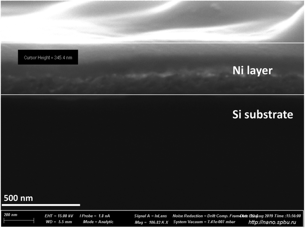 | ||
| Fig. 3 SEM image of a cross-cleavage of the Ni-coated silicon plate used for the depth profiling study (Fig. 4). Ni film thickness is 345.4 nm, according to SEM measurements. | ||
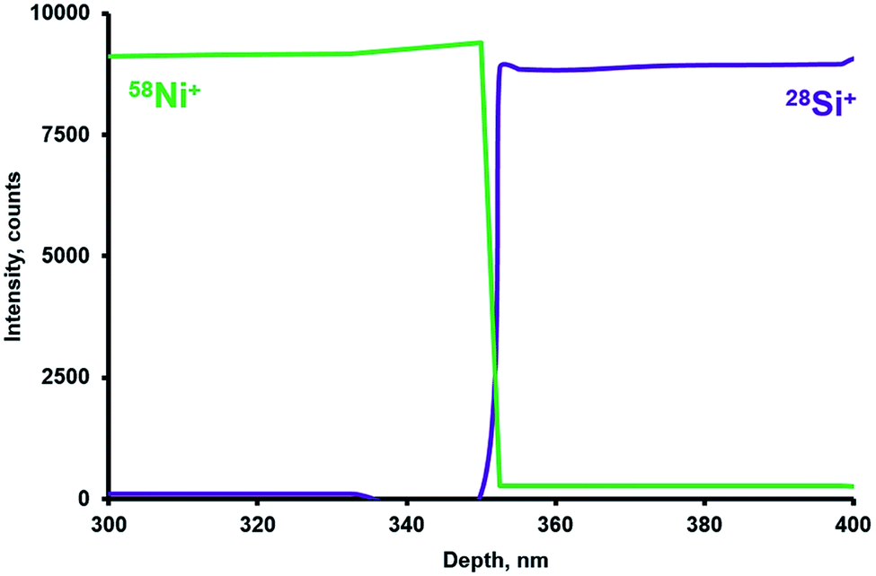 | ||
| Fig. 4 A sputtering profile of the 350 nm Ni coated Si plate. Sputtering parameters are as follows: pressure 42.6 Pa, pulse duration 4 μs, discharge voltage 1300 V, repelling pulse delay 200 μs, and Ta auxiliary cathode. Acquisition period 0.62 s (2000 mass spectra packet per point), and the data are converted to the profile by depth based on the sputtering rate. | ||
A sharp transition from Ni to Si observed (Fig. 4) indicates high depth resolution of the sputtering. The calculation (based on the interfacial distance between 16 and 84% intensities according to Morrison et al.48) resulted in a depth resolution of ca. 5 nm. The obtained value seems competitive compared to those obtained for other systems mentioned in the literature.3,9,13,15,21,47 Importantly, such a resolution value was obtained for the crater depth of 350 nm (Ni film thickness). This indicates a slow deterioration of depth resolution with the crater depth for conducting samples.
3.4 Semiconducting films on a dielectric support
The possibility to undertake depth analysis for multilayer semiconductor–dielectric systems was studied using the sample of borosilicate glass coated with a silicon layer of 658 nm (Si/borosilicate glass). The thickness was measured by SEM. The sample of Si/borosilicate glass was provided by the Ioffe Physical-Technical Institute (St. Petersburg, Russia). The material originated from the testing of a new magnetron design. The novel magnetron regime under development enables the deposition of coatings on wider areas with higher speed, due to the wider distribution of the electromagnetic field. In the current study, to test the magnetron-produced material, it was necessary to validate the absence of impurities in the coating, originating from the materials of the magnetron setup. The magnetic circuit and a special protective case of the magnetron may contaminate the sample with such metals as silver, copper, and nickel. Since silver was an analyte of interest, the sample was preliminarily coated with a 170 nm layer of Ta (Fig. 5). The depth profile for potential impurities in the silicon layer was acquired under optimized conditions (Fig. 6). After complete sputtering of the silicon coating, the effective sputtering of the borosilicate support was observed (which is represented by the intensity profiles of boron and calcium in Fig. 6(a)). Ta and Si layers initiate the formation of surface conductivity, which later becomes self-reproducing for the dielectric support.40,41 The data in Fig. 6 indicate that the Si coating of the specimen has a considerable amount of impurities, originating from the magnetron setup since quite high intensities of 107Ag+, 63Cu+, and 58Ni+ were observed. Interestingly, in the initial phase of coating of the borosilicate plate, the main contribution to the coating's contamination was related to silver, mainly originating from the protective case, while later mainly copper and nickel from the magnetic circuit were present (observed in reversed order in the sputtering profile). The corresponding SEM image and SEM EDX maps of the crater surface similar to those shown in Fig. 2 are presented in Fig. S2 (ESI†). | ||
| Fig. 5 SEM image of a cross-cleavage of the Si coating on the FIOLAX 8412 borosilicate glass support (the thickness of the layer considered was 500 nm) before (a) and after (b) the Ta coating was deposited. The total thickness of the Si layer was 658 nm, and the added Ta coating was 170 nm thick. | ||
 | ||
| Fig. 6 (a) Qualitative depth profile and (b) quantitative depth profile for 658 nm Si/borosilicate glass with a preliminary deposited 170 nm layer of Ta. Discharge conditions are as follows: pressure 42.6 Pa, pulse duration 4 μs, repelling pulse delay 200 μs, power 1300 V, and Ta auxiliary cathode. | ||
The preliminary coating of the semiconductor–dielectric multilayer system with a thin metallic layer introduces three main benefits: (i) this layer equalizes the surface potential improving the crater shape, as it was demonstrated for the silicon plate (Fig. 4); (ii) for non-conducting materials, the metallic layer initiates the sputtering and induces the formation of self-reproducing surface conductivity; (iii) this layer sheathes the sample in the initial phase of sputtering during the discharge stabilization and removal of cell's contaminants, first of all, related to moisture. The acquired data (Fig. 6(a)) demonstrate that during the sputtering of the Ta coating the signals of water-associated clusters 1H16O+, 1H216O+, and 1H316O+, as well as the intensity of 12C+, decreased considerably. The aspects (ii) and (iii) are further illustrated in Fig. 8.
The presence of water and atmospheric gases in the cell is nearly inevitable. These and sample surface contamination seriously affect the discharge stability, deteriorating the depth analysis during the initial phase of the profiling. Molchan et al.49 offered two strategies to cope with those effects: preliminary cleaning of the sample surface with a short low power discharge and preliminary sputtering of the “sacrificial material”; single-crystal silicon was used in this case. In the current study, these approaches were also tested and showed their efficiency. However, we proposed an additional sample preparation strategy – the deposition of a thin layer of metallic silver on the sample. Such sample coating may be considered as the use of a “sacrificial material” in situ. Importantly, after the sputtering of the silver layer, the interface remained rather sharp (Fig. 6); i.e., such sample treatment did not affect the depth resolution considerably. The required thickness of the deposited metal layer may be varied based on the sample under study, its conductivity and surface quality.
For the Si/borosilicate glass specimen, semi-quantitative profiles of Ag, Cu, and Ni were obtained (Fig. 6(b)). RSFs were measured using a certified reference material of copper no. 9410 (state standard no. 3519-86, Russia). To validate the profiling results, the average content of the admixtures in the film was compared with the SEM EDX results at an accelerating voltage of 5 keV. The accelerating voltage was optimized to effectively excite the X-ray spectra of the elements of interest to the maximal depths of the film without involving the glass support. The data for the current technique (CHC μs-DC-PGD TOFMS) and SEM EDX are presented in Table 2. The data between the two techniques were in concordance, indicating the absence of considerable systematic errors for the quantitative depth profiling. Unfortunately, the lack of appropriate validation standards did not allow us to claim the complete quantification at this point. However, the prospect to undertake quantitative analysis with the results comparable to SEM EDX was strongly demonstrated.
| Element | SEM-EDX | CHC μs-DC-PGD TOFMS |
|---|---|---|
| Ag, at% | 9.4 ± 1.1 | 9.1 ± 0.5 |
| Cu, at% | 3.2 ± 0.5 | 2.87 ± 0.19 |
| Ni, at% | 0.9 ± 0.4 | 1.14 ± 0.15 |
3.5 Dielectric multilayer coatings
The possibility of profiling of dielectric multilayer coatings on a dielectric support was investigated using two specimens of reflective dielectric multilayer (mirror) coatings: 100 nm SiO2–100 nm TiO2–(140 nm SiO2–100 nm TiO2) × 14 and 55 nm SiO2–85 nm TiO2–(120 nm SiO2–85 nm TiO2) × 14, both on a glass support. The layer thicknesses were measured using SEM with a backscattering electron detector (BSE) in a preliminary experiment (Fig. 7). | ||
| Fig. 7 SEM images of a cross-cleavage of the multilayer coatings on a glass support. A backscattered electron detector, sensitive to atomic mass, was used. Dark lines are attributed to Si; light lines are attributed to Ti. The layer thicknesses are as follows: (a) 100 nm for Ta, 85 nm for titanium dioxide, and 120 nm for silicon dioxide; (b) 65 nm for silver, 100 nm for titanium dioxide, and 140 nm for silicon dioxide. | ||
For the sputtering of dielectrics in μs-pulsed glow discharge, the formation of surface conductivity is required.37 The surface conductive layer may be formed on the sample by preliminary coating its surface with a thin metallic (Ag, Ta, etc.) layer. The sputtering starts with this coating and then proceeds to the sample per se. The sputtering continues due to the induced surface conductivity related to the depletion of the sample surface with an easily sputtered component. In the case of our multilayer mirror specimens, the sample surface was depleted of oxygen thus being enriched in more hardly sputtered Ti and Si.
Initially, to improve sample sputtering, we tested Ta 100 nm layer deposition on the sample surface. However, such sample preparation caused accelerated deterioration of the depth resolution (Fig. 8(a)). The substantial deterioration of the depth resolution for Ta was observed for the depth of ca. 1500 nm. Based on the experiments with Si plates (Fig. 1), the deposition of the Ag layer (60 nm) was tested to cope with fast depth resolution deterioration. The use of silver resulted in stable sputtering of all layers of the sample up to the depth of several micrometers with a slow decrease of the resolution with the depth. The corresponding profile is presented in Fig. 8(b). Thus, the analytical system used could distinctly resolve all 31 layers of the sample.
 | ||
| Fig. 8 A qualitative depth profile for the 55 nm SiO2–85 nm TiO2–(120 nm SiO2–85 nm TiO2) × 14 multilayer (IR-mirror) coating on a glass support measured under the following conditions: pressure 42.6 Pa, pulse duration 4 μs, repelling pulse delay 200 μs, power 1300 V, and Ta CHC with a preliminary deposited 100 nm Ta layer (a) or 60 nm Ag layer (b). 107Ag+ intensity was multiplied by a factor of 0.1; 1H316O+ intensity was multiplied by a factor of 10. | ||
The better performance of Ag compared to Ta may be attributed to the significantly higher sputtering efficiency of Ag,50 which correlates with the lower enthalpy of evaporation. Ag has a lower ionization energy (7.5 for Ag and 7.8 eV for Ta, respectively) so it can be more easily ionized by the cascade mechanism engaged by low metastable levels with the energies of ca. 0.7 and 1.4 eV.51 A possible mechanism explaining the better performance of Ag is related to the increased concentration of charged particles in the proximal zone to the sample surface compared to Ta, resulting in higher field homogeneity flattening the crater shape.
Thus, to ensure effective sputtering of consequential layers of SiO2 and TiO2 on the glass support, the sample surface was covered with the thin layer of metallic silver (thickness 65 nm). The presence of the silver layer resulted in homogeneous sputtering of the layers without the presence of water-associated clusters in the mass spectrum (1H16O+, 1H216O+, and 1H316O+) during the sputtering of the sample per se. The interference was present only during the sputtering of the Ag coating (demonstrated in Fig. 8(b) for the most intensive cluster 1H316O+). Getter properties of the Ta hollow cathode additionally reduced water- and oxygen-associated cluster formation.44–46 In principle, the Al hollow cathode was also applicable to the task. However, in the case of Al, the lack of getter properties resulted in a slower reduction of interference. Additionally, the use of Al resulted in a lower depth resolution compared to Ta and only a few first layers could be distinguished (data not shown). To conclude, when comparing Ta (Fig. 8(a)) and Ag deposited layers (Fig. 9) for the study of multilayer films, the clear benefit of Ag was identified.
 | ||
| Fig. 9 Qualitative depth profile (28Si+, 48Ti+, 107Ag+, and 16O+ intensities vs. depth) for the 100 nm SiO2–100 nm TiO2–(140 nm SiO2–100 nm TiO2) × 14 multilayer (IR-mirror) coating on glass measured under the following conditions: pressure 42.6 Pa, pulse duration 4 μs, repelling pulse delay 4 μs, power 1300 V, and Ta CHC with a preliminary deposited 65 nm Ag layer. | ||
The use of a Ta CHC with a preliminary deposited Ag layer on the sample surface provides homogeneous sputtering of the layers up to the depth of several micrometers with a depth resolution of 8 nm at the depth up to 60 nm and 25 nm at the depth of 1000 nm. Additionally, under short repelling pulse delay, the effective electron ionization mechanism enabled the quantification of high ionization energy elements,39–41Fig. 7(a), (b) and 8(a) and (b) demonstrate the profiling of all main components of the coatings, including oxygen.
The deterioration of depth resolution during the sputtering is a substantial common problem in GDOES and GDMS profiling. It was previously observed by a number of authors.20,25,32,35,47 Importantly, in the current study, up to the depth of several micrometers, every layer could be resolved (Fig. 9). The achieved resolution (5–8 nm) for relatively shallow craters of tens of nanometers is comparable to that attainable in Grimm cell glow discharge.9 For the deeper craters of about 1000 nm, the resolution (25 nm) is also comparable to that obtained in the Grimm cell.25,26 The amplitudes for the intensity maxima in Fig. 8 and 9 visually decrease with time, while the baseline intensity increases. Similar trends caused by depth resolution worsening with depth were also observed for the Grimm cell.3,20,47,52 The use of the auxiliary cathode (an additional metallic cylinder), in principle, may have further worsened depth resolution due to the potential redisposition of the sample matter on the auxiliary cathode with its consequent sputtering into the plasma. Nevertheless, the magnitude of the intensity minimum following the first maximum exceeds 95%, which demonstrates a low potential contribution of such a “memory effect”.
4. Conclusion
The current study shows the applicability of CHC μs-DC-PGD TOFMS for depth profiling of different chemical compositions and electrical conductivities – conductors, semiconductors, and dielectrics. For the sputtering of dielectrics, including multilayer coatings, the deposition of a thin metallic layer (Ag or Ta) on the sample surface was proposed. Such sample pre-treatment improved the formation of surface conductivity, self-reproducing during the sputtering and reduced the effect of adsorbed atmospheric components and water at the initial phase of analysis. Ag deposition on the sample surface was demonstrated to provide the optimal depth resolution under stable sputtering. The prospect of quantitative profiling was demonstrated on silicon-coated borosilicate glass. High depth resolution (5 nm for conducting materials and 8 nm for dielectrics at the depth of 60 nm, increasing to 25 nm by the depth of 1000 nm) was obtained for the coatings from several tens of nanometers to several micrometers.Conflicts of interest
There are no conflicts to declare.Acknowledgements
The research has been supported by a grant from the Russian Science Foundation (grant No. 17-73-20089). The authors are grateful to the Interdisciplinary Resource Centre for Nanotechnology (St. Petersburg State University, St. Petersburg, Russia) for providing access to their facilities. The authors would also like to thank Dr Volker Hoffmann for his help with measurements of crater profiles and the Ioffe Physical-Technical Institute for providing some of the samples.References
- Glow Discharge Plasmas in Analytical Spectroscopy, ed. R. K. Marcus and J. A. C. Broekaert, John Wiley & Sons, Ltd, Chichister, England, 2003 Search PubMed.
- L. Lobo, B. Fernández and R. Pereiro, J. Anal. At. Spectrom., 2017, 32, 920–930 RSC.
- R. Escobar Galindo, R. Gago, D. Duday and C. Palacio, Anal. Bioanal. Chem., 2010, 396, 2725–2740 CrossRef CAS PubMed.
- S. Mohajernia, A. Mazare, I. Hwang, S. Gaiaschi, P. Chapon, H. Hildebrand and P. Schmuki, Appl. Surf. Sci., 2018, 442, 412–416 CrossRef CAS.
- P. Jonnard, M. H. Modi, K. Le Guen, N. Aneshwari, M. Sinha, M. Idir, P. Chapon and A. Galtayries, Surf. Interface Anal., 2018, 50, 1213–1217 CrossRef CAS.
- M. Di Sabatino, C. Modanese and L. Arnberg, J. Anal. At. Spectrom., 2014, 29, 2072–2077 RSC.
- C. Modanese, L. Arnberg and M. Di Sabatino, Mater. Sci. Eng., B, 2014, 180, 27–32 CrossRef CAS.
- R. Muniz, L. Lobo, T. Kerry, C. A. Sharrad and R. Pereiro, J. Anal. At. Spectrom., 2017, 32, 1306–1311 RSC.
- J. Pisonero, N. Bordel, C. González de Vega, B. Fernández, R. Pereiro and A. Sanz-Medel, Anal. Bioanal. Chem., 2013, 405, 5655–5662 CrossRef CAS PubMed.
- A. Bengtson, Spectrochim. Acta, Part B, 1994, 49, 411–429 CrossRef.
- A. Bengtson and S. Hänström, ISIJ Int., 2002, 42, S82–S85 CrossRef CAS.
- T. Nelis and J. Pallosi, Appl. Spectrosc. Rev., 2006, 41, 227–258 CrossRef CAS.
- J. Pisonero, B. Fernández, R. Pereiro, N. Bordel and A. Sanz-Medel, TrAC, Trends Anal. Chem., 2006, 25, 11–18 CrossRef CAS.
- K. Shimizu, H. Habazaki, P. Skeldon and G. E. Thompson, Surf. Interface Anal., 2003, 35, 564–574 CrossRef CAS.
- K. G. Reinsberg, C. Schumacher, A. Tempez, K. Nielsch and J. A. C. Broekaert, Spectrochim. Acta, Part B, 2012, 76, 175–180 CrossRef CAS.
- B. Ber, P. Bábor, P. N. Brunkov, P. Chapon, M. N. Drozdov, R. Duda, D. Kazantsev, V. N. Polkovnikov, P. Yunin and A. Tolstogouzov, Thin Solid Films, 2013, 540, 96–105 CrossRef CAS.
- I. Spitsberg and K. Putyera, Surf. Coat. Tech., 2001, 139, 35–43 CrossRef CAS.
- W. Luesaiwong and R. K. Marcus, J. Anal. At. Spectrom., 2004, 19, 345–353 RSC.
- H. Takahara, M. Shikano and H. Kobayashi, J. Power Sources, 2013, 244, 252–258 CrossRef CAS.
- S. Oswald and S. Baunack, Thin Solid Films, 2003, 425, 9–19 CrossRef CAS.
- D. Abou-Ras, R. Caballero, C. Streeck, B. Beckhoff, J.-H. In and S. Jeong, Microsc. Microanal., 2015, 21, 1644–1648 CrossRef CAS PubMed.
- J. Greene and J. Whelan, J. Appl. Phys., 1973, 44, 2509–2513 CrossRef CAS.
- A. Tempez, S. Legendre and P. Chapon, Proc. SPIE, 2013, 8626, 08 CrossRef.
- A. Tempez, S. Legendre and P. Chapon, Nucl. Instrum. Methods Phys. Res., Sect. B, 2014, 332, 351–354 CrossRef CAS.
- R. Muñiz, L. Lobo, K. Németh, L. Péter and R. Pereiro, Spectrochim. Acta, Part B, 2017, 135, 34–41 CrossRef.
- A. Alvarez-Toral, P. Sanchez, A. Menéndez, R. Pereiro, A. Sanz-Medel and B. Fernández, J. Am. Soc. Mass Spectrom., 2015, 26, 305–314 CrossRef CAS PubMed.
- M. Vázquez Peláez, J. Pisonero, J. M. Costa-Fernández, R. Pereiro, N. Bordel and A. Sanz-Medel, J. Anal. At. Spectrom., 2003, 18, 612–617 RSC.
- N. Baguer and A. Bogaerts, J. Appl. Phys., 2005, 98, 033303 CrossRef.
- L. O. Actis-Dato, L. Aldave de Las Heras, M. Betti, E. H. Toscano, F. Miserque and T. Gouder, J. Anal. At. Spectrom., 2000, 15, 1479–1484 RSC.
- C. L. Lewis, M. A. Moser, D. E. Dale, W. Hang, C. Hassell, F. L. King and V. Majidi, Anal. Chem., 2003, 75, 1983–1996 CrossRef CAS PubMed.
- J. Pisonero, R. Valledor, A. Licciardello, C. Quirós, J. I. Martín, A. Sanz-Medel and N. Bordel, Anal. Bioanal. Chem., 2012, 403, 2437–2448 CrossRef CAS PubMed.
- R. Escobar Galindo, E. Forniés and J. M. Albella, J. Anal. At. Spectrom., 2005, 20, 1116–1120 RSC.
- R. Valledor, J. Pisonero, N. Bordel, J. I. Martín, C. Quirós, A. Tempez and A. Sanz-Medel, Anal. Bioanal. Chem., 2010, 396, 2881–2887 CrossRef CAS PubMed.
- L. Lobo, J. Pisonero, N. Bordel, R. Pereiro, A. Tempez, P. Chapon, J. Michler, M. Hohl and A. Sanz-Medel, J. Anal. At. Spectrom., 2009, 24, 1373–1381 RSC.
- R. Escobar Galindo, E. Forniés and J. M. Albella, J. Anal. At. Spectrom., 2005, 20, 1108–1115 RSC.
- R. B. Djulgerova, L. I. Popova, V. I. Mihailov, G. D. Beshkov, A. Szytula, L. Gondek and Z. Lj. Petrovic, Spectrochim. Acta, Part B, 2004, 59, 905–908 CrossRef.
- A. Gubal, A. Ganeev, V. Hoffmann, M. Voronov, V. Brackmann and S. Oswald, J. Anal. At. Spectrom., 2017, 32, 354–366 RSC.
- A. Ganeev, A. Gubal, V. Mosichev, N. Pershin, V. Bichaev, V. Malyshev, S. Potapov and K. Uskov, J. Russ. Soc. Mass Spectrom. “Mass-Spectrometria”, 2012, 9, 269–276 CAS.
- A. Ganeev, A. Gubal, V. Chuchina, Y. Lyalkin, O. Glumov, V. Yakobson and N. Solovyev, J. Anal. At. Spectrom., 2019, 34, 588–597 RSC.
- A. Gubal, A. Ganeev, V. Bodnar, N. Solovyev, Y. Lyalkin, O. Glumov and V. Yakobson, Vacuum, 2018, 153, 248–253 CrossRef CAS.
- V. Bodnar, A. Ganeev, A. Gubal, N. Solovyev, O. Glumov, V. Yakobson and I. Murin, Spectrochim. Acta, Part B, 2018, 145, 20–28 CrossRef CAS.
- A. Ganeev, A. Gubal, B. Korotetski, O. Bogdanova, B. Burakov, A. Titova, N. Solovyev, N. Ivanenko, E. Drobyshev, E. Iakovleva and M. Sillanpää, Microchem. J., 2017, 132, 286–292 CrossRef CAS.
- S. Potapov, E. Izrailov, V. Vergizova, M. Voronov, S. Suprunovich, M. Slyadnev and A. Ganeev, J. Anal. At. Spectrom., 2003, 18, 564–571 RSC.
- Y. Mei and W. W. Harrison, Spectrochim. Acta, Part B, 1991, 46, 175–182 CrossRef.
- M. Betti and L. Aldave de las Heras, Spectrochim. Acta, Part B, 2004, 59, 1359–1376 CrossRef.
- A. A. Ganeev, A. R. Gubal, S. V. Potapov, S. E. Pogarev, S. E. Sholupov, K. N. Uskov and I. S. Ivanov, J. Anal. Chem., 2013, 68, 1205–1211 CrossRef CAS.
- M. Wilke, G. Teichert, R. Gemma, A. Pundt, R. Kirchheim, H. Romanus and P. Schaaf, Thin Solid Films, 2011, 520, 1660–1667 CrossRef CAS.
- G. H. Morrison, K. L. Cheng and M. Grasserbauer, Pure Appl. Chem., 1979, 51, 2243–2250 Search PubMed.
- I. S. Molchan, G. E. Thompson, P. Skeldon, N. Trigoulet, P. Chapon, A. Tempez, J. Malherbe, L. Lobo Revilla, N. Bordel, P. Belenguer, T. Nelis, A. Zahri, L. Therese, P. Guillot, M. Ganciu, J. Michler and M. Hohl, J. Anal. At. Spectrom., 2009, 24, 734–741 RSC.
- N. Laegreid and G. Wehner, J. Appl. Phys., 1961, 32, 365–369 CrossRef CAS.
- A. Kramida, Yu. Ralchenko, J. Reader and NIST ASD Team, NIST Atomic Spectra Database (ver. 5.5.2), online, available: https://physics.nist.gov/asd, accessed February 22, 2018, available: https://physics.nist.gov/asd, 2018, February 22 Search PubMed.
- V.-D. Hodoroaba, W. E. S. Unger, H. Jenett, V. Hoffmann, B. Hagenhoff, S. Kayser and K. Wetzig, Appl. Surf. Sci., 2001, 179, 30–37 CrossRef CAS.
Footnote |
| † Electronic supplementary information (ESI) available. See DOI: 10.1039/d0ja00088d |
| This journal is © The Royal Society of Chemistry 2020 |