
 Open Access Article
 This Open Access Article is licensed under a
 Creative Commons Attribution 3.0 Unported Licence
Patterning of metal oxide thin films using a H2/He atmospheric pressure plasma jet†
M. Emre
Sener
,
Sanjayan
Sathasivam
 ,
Robert
Palgrave
,
Raul
Quesada Cabrera
and
Daren J.
Caruana
*
,
Robert
Palgrave
,
Raul
Quesada Cabrera
and
Daren J.
Caruana
*
Department of Chemistry, Christopher Ingold Laboratories, University College London, 20 Gordon St., London, WC1H 0AJ, UK
First published on 7th February 2020
Abstract
A hydrogen-doped helium atmospheric pressure plasma jet (APPJ) is shown to be effective for the chemical reduction of metal oxides. Copper and tin oxide films (CuO and SnO2) show rapid (<2 seconds) and complete reduction to zero valence metal after exposure to the plasma jet, as revealed by X-ray photoelectron spectroscopy (XPS), Auger electron spectroscopy, and Raman spectroscopy. After a total residence time of the plasma jet of 100 seconds, titanium oxide (TiO2) produced a surface decorated with Ti2+, Ti3+ and Ti4+ with proportions of 16, 38 and 46 atom%, respectively, as determined by XPS peak integration. Similarly, with tungsten oxide (WO3), after exposure for a few seconds, W5+ was produced, yielding a deep blue electrically conductive coating. The treatment of these oxide films by this dielectric radio frequency (RF) barrier discharge plasma jet provides a level of redox conversion not seen in any other technique, particularly for TiO2, especially with a comparable power input. The precise nature of the reduction is unclear; however, the involvement of free electrons may have an important role in the reduction process.
Introduction
Gaseous plasmas are potent chemically reactive environments containing a rich mixture of highly reactive radicals and ions, including free electrons. Remarkably, most plasmas are produced from the most unreactive inert gas by the injection of sufficient energy to ionise the gas, producing a sustained reactive ionised gas. The upshot of this, from a sustainability aspect, is that the starting material is an inert gas and the product is the same inert gas, as little of the gas is actually consumed. Yet harnessing the reactive power of plasmas can yield a very accessible and clean chemical processing approach.1,2In this publication, we demonstrate that a low power (<50 W) atmospheric pressure plasma jet (APPJ) alters the redox state of metal oxide thin films. This approach offers a significant benefit in purposeful materials processing and surface patterning, to achieve differential surface properties using a clean and energy efficient APPJ technique.3
Metal oxides are some of the most thermodynamically stable materials with uninteresting chemistry. Their surface, on the other hand, can support a very rich chemistry; in fact, many metal oxides have been harnessed as catalytic materials primarily due to their surface reactivity. Enhancing or refining the surface chemistry often involves chemical modification of both the surface and the bulk, typically using techniques such as doping during the synthesis, focused lasers and molecular beams. These techniques are often power-hungry and/or expensive to access, e.g. using vacuum systems.4 So accessible techniques utilising materials that are sustainable and benign are a priority.
Thermal plasmas, such as flames, where the electron temperature is roughly equal to the temperature of the neutral species, can promote redox reactions at a solid surface, as demonstrated using the electrochemical methodology.5 Non-thermal plasmas, on the other hand, can be stabilised away from the thermal equilibrium; in most cases, electrons are orders of magnitude more energetic than the neutral species contained in the plasma gas. Plasma chamber chemical treatment studies have demonstrated an impressive array of chemical control, for example, by Stuckert et al. and Schade et al.6 who demonstrated the complete reduction of Sn4+ to Sn0 in a hydrogen- or water-doped argon plasma. Yan et al. and Wang et al. have described the hydrogenation of TiO2 to produce TiO2 black in a plasma chamber for photocatalytic applications.7 Plasma reduction of copper oxide layers to metallic copper in a low pressure H2/He plasma has been described by Sawada et al.8 and Sabat et al.9 Also Inui et al.10 demonstrated CuO and Cu2O reduction in a H2/Ar atmospheric pressure plasma. In all these studies, hydrogen radicals present in the doped plasma were implicated in the reduction process. The work of Di et al. has demonstrated the reduction of some metal ions (Au, Pd, Ag and Pt) using alcohol11 and CO12 cold plasmas, in the absence of hydrogen.13
However, plasmas are an accessible source of free electrons, and as a consequence, they have been implicated to be effective at driving chemical change at liquid, soft solid and solid surfaces.5b,14 Richmonds, Brettholle and Meiss demonstrated charge-transfer processes at the plasma/liquid interface by positioning a plasma discharge in contact with a liquid electrolyte.15 More recently, Hawtof and co-workers were able to demonstrate the formation of ammonia in water, showing that electrons can indeed cross the plasma–liquid interface in a discharge plasma.16 We have shown that helium plasma at atmospheric pressure in the absence of hydrogen was effective at reducing copper oxide films, suggesting that electrons alone are, in the case of copper, sufficient for the reduction process.17 This view is supported by Lee et al.18 and Sui et al.19 who loaded metal ions in a polymer matrix and showed using an APPJ that the reduction of the metal ions was indeed driven by plasma (or secondary) electrons.
In this investigation, the treatment of metal oxides using an APPJ is shown to affect the reduction of metal oxides. Specifically, stable metal oxide films are shown to be rapidly reduced with non-thermal plasmas under mild conditions. Using an in-house designed and built helium plasma jet doped with hydrogen, it is shown for the first time that coatings of TiO2, WO3 and ZnO resulted in mixed valence materials after exposure to plasma, and SnO2 and Cu2O may be completely reduced to the metal via plasma exposure, as schematically shown in Fig. 1.
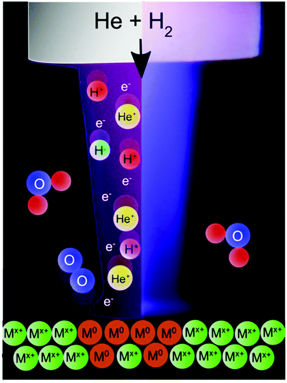 | ||
| Fig. 1 Schematic image of an atmospheric pressure plasma jet showing the plasma components impinging on a metal oxide surface leading to the reduction process. | ||
Results and discussion
In this study, five metal oxide thin films were tested, and the films were deposited using aerosol-assisted chemical vapour deposition (TiO2, SnO2, WO3, and ZnO) or electrochemical deposition (Cu2O) (see the ESI† for details). For each of the five metal oxide materials tested, a detailed analysis of the XPS, Auger and Raman spectra was performed for the pristine coating and the coating exposed to the plasma jet for various lengths of time. In some cases, the morphology change upon exposure to the plasma was characterised by SEM.Electrodeposited copper oxide (Cu2O) films showed clear evidence of reduction from Cu+ to Cu0 even after one pass (over a distance of 5 mm at a rate of 1 mm s−1) of the plasma jet. The photograph in Fig. 2a shows the metallic copper tracks on the red Cu2O surface produced via the plasma treatment of the surface after one, two, three and five passes of the plasma jet. The SEM images of the surface before, Fig. 2b, and after, Fig. 2c, show that there is a very slight change in the morphology of the cubic Cu2O crystalline structure due to the plasma treatment. The substrate temperature, measured with a non-contact thermometer, did not increase beyond 5 °C above ambient temperature, highlighting the gentle nature of the plasma jet treatment process.
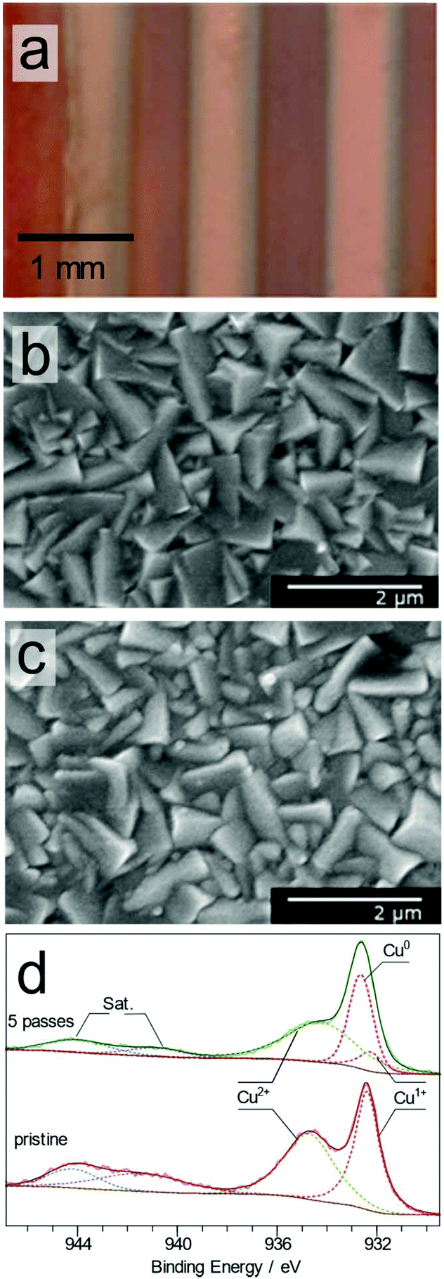 | ||
| Fig. 2 Photograph of the plasma treated Cu2O surface after 1, 2 and 5 passes (a). SEM image of the as-deposited, crystalline Cu2O film (b) and the surface after 5 passes of the plasma jet (c). High resolution XPS Cu 2p spectra of the as-deposited and plasma treated surface (d). | ||
The XPS spectra of the Cu 2p photoelectron region at high resolution for the as-deposited Cu2O surface and after the plasma treatment are shown in Fig. 2d. The main peaks of the spectra are located around 932 and 952 eV, due to the photoelectron emission from the Cu 2p3/2 and 2p1/2 levels, respectively. The Cu 2p3/2 spectrum obtained from the pristine surface can be modelled with two main components centered at 932.3 and 934.7 eV with FWHM values of 1.2 and 2.8 eV. The peak at 932.3 eV is assigned to Cu2O, while the higher binding energy peak is attributed to Cu(OH)2.20 Shake-up satellite features, labeled as Sat. in Fig. 2d, are observed; these features are mainly due to the presence of Cu(II) species on the surface.21 The Cu 2p3/2 spectrum obtained from the plasma treated surface at five passes shows significant changes compared with the pristine surface (Fig. S1†): the spectral intensity of the low binding energy feature around 932.7 eV increased compared with the higher binding energy feature around 934.7 eV, suggesting reduction of the surface by the plasma. This region was modelled with three Cu 2p3/2 components in addition to two components due to shake-up processes. The modelled components located at 932.3, 932.6, and 934.7 eV are assigned to the species Cu2O, Cu, and Cu(OH)2, respectively, based on the published binding energies.20 The metallic copper peak at 932.6 eV is present only in the plasma exposed areas, showing that the plasma treatment results in rapid reduction of Cu2O into metallic Cu. The presence of Cu(I) and Cu(II) species is attributed to the thin native oxide layer formed on the copper surface upon exposure to ambient air during handling.
Raman spectra of the pristine film showed characteristic bands of Cu2O at 220 and 630 cm−1 (Fig. S2†).22 Raman spectra collected from various points extending from the center of the reduced copper track showed no copper oxide. This confirmed that the Cu2+ species seen in the XPS spectra are due to a thin (<1 μm) layer of native oxide formed upon exposure to air after the plasma treatment. To confirm the presence of metallic copper, Cu LMM Auger electron spectra from the samples were acquired (Fig. S3†). The pristine surface showed a single Auger peak at 916.9 eV electron energy. This peak was composed of unresolved contributions from both Cu(OH)2 and Cu2O.21 The plasma treated surfaces, in contrast, showed a second peak at 918.5 eV, characteristic of metallic copper.23
Titanium dioxide (TiO2) is known to be an extremely robust and chemically stable oxide, yet exposure to plasma showed a clear transformation from the characteristic white as-deposited TiO2 to blue or off-white, as shown in Fig. 3a and b. Ti 2p XPS spectra showed two major peaks with spin–orbit splitting of 5.7 eV and an intensity ratio of 2![[thin space (1/6-em)]](https://www.rsc.org/images/entities/char_2009.gif) :1, Fig. 3c. The Ti 2p3/2 peak for the pristine surface is centred at 458 eV with a FWHM value of 1.16 eV, in agreement with the reference values.24
:1, Fig. 3c. The Ti 2p3/2 peak for the pristine surface is centred at 458 eV with a FWHM value of 1.16 eV, in agreement with the reference values.24
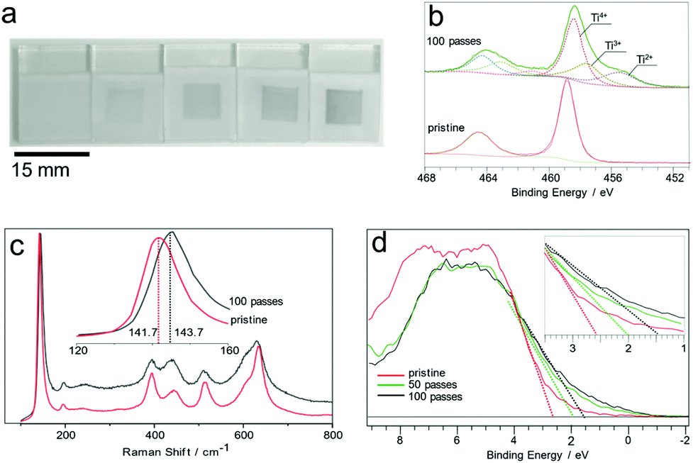 | ||
| Fig. 3 Photographs of the pristine and treated TiO2 films showing 7 × 7 mm areas treated by raster scanning the plasma jet over the surface 0 to 100 times in increments of 25; the leftmost sample shows the pristine white surface prior to treatment (a). Ti 2p spectra of the TiO2 surface before and after plasma exposure (b). Raman spectrum of the treated and untreated surfaces (c). Valence band spectrum of the TiO2 surface (d). | ||
Plasma treated surfaces display a major shift of the Ti 2p main peak from 458.8 to 458.1 eV beyond 50 passes of the plasma jet over the surface. Furthermore, a prominent feature at 455.5 eV appeared and grew with longer plasma treatment durations. This was ascribed to Ti2+ species formed via reduction, as shown in Fig. 3c. The O 1s spectra of the samples (Fig. S4†) show two distinct peaks. The high binding energy peak (Oads) at 530.8 eV was assigned to surface OH, and C–O contaminants. The lower binding energy peak (Olat) at 529.5 eV was assigned to TiO2 lattice oxygen. The values for these two components are in line with the reference values reported for TiO2. The valence band region of the TiO2 XPS spectrum shows a significant downward shift of the valence band maximum from 2.4 to 1.2 eV. This shift is found to increase in magnitude with increasing treatment time; see Fig. S5.† Raman analysis of the surface showed the characteristic band structure arising from the anatase/rutile phase mixture (Fig. 3d). Interestingly, the treated spots show distinct broadening and a 2 cm−1 blue-shift of the anatase Eg band from 141.7 cm−1 to 143.7 cm−1, which has been previously reported in the literature as an indicator of oxygen vacancies in the anatase structure.25 The plasma modified surface was found to be air-stable for at least 4 months at room temperature and completely reversed by annealing in air leading to recovery of the original XPS and Raman spectra.
Plasma treated tin dioxide (SnO2) thin films showed a distinct change in appearance, turning opaque and brown in colour, Fig. 4a. This change in appearance depends on the overall plasma treatment time. Inspection of the SEM images of the surface, Fig. 4b and c, suggests that the likely reason behind this change in optical properties is the evolution of Sn “beads” on the surface.
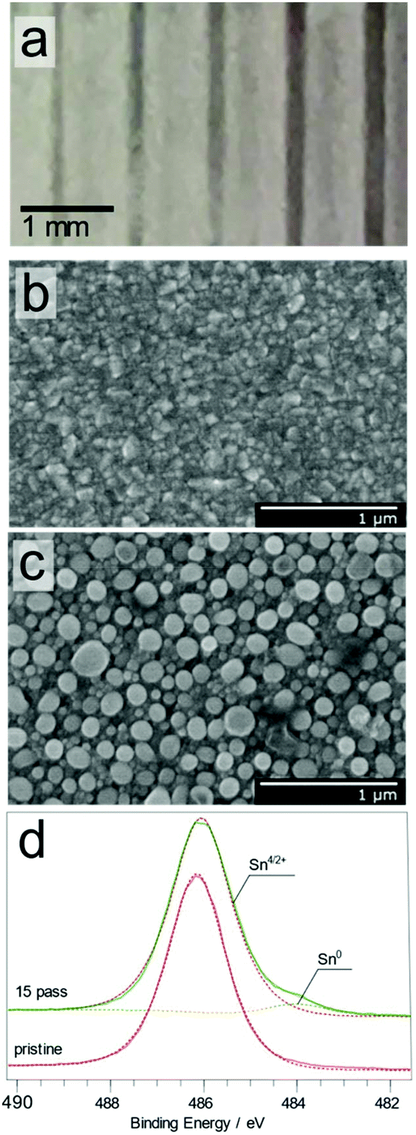 | ||
| Fig. 4 Photograph of the plasma treated SnO2 surface from 5 to 25 passes in increments of 5 (a). SEM image of the as-deposited, crystalline SnO2 film (b) and the surface after 15 passes of the plasma jet (c). High resolution XPS Sn 3d spectra of the as-deposited and plasma treated surface (d). | ||
The Sn 3d3/2 and 3d5/2 peaks showed significant changes in both position and full width at half-maximum (FWHM) (as shown in Fig. S6†), as the number of plasma passes increased (0, 5, 10, 15, 20 and 25).26 This peak shift and peak broadening were attributed to the presence of sub-oxides on the surface. Furthermore, the deconvoluted Sn 3d5/2 spectra showed that the plasma treatment resulted in the appearance of two major photoelectron peaks at 486.1 and 484.2 eV, Fig. 4d and Fig. S6†. These peaks can be assigned to the SnO2 and Sn species on the surface, respectively, consistent with the published values,26,27 demonstrating that Sn4+ was reduced to Sn0 upon plasma exposure. These results are in good agreement with the previous studies of surfaces exposed to low pressure H2 plasmas.28,6c It is important to note that the binding energy value of 484.2 eV obtained for metallic tin is significantly lower than the commonly reported reference value of 485.0 eV, but agrees with the previously published values reported for plasma reduced surfaces.6a,c,28 Also the oxygen XPS spectrum for SnO2 showed a shift in Olat, which is also consistent with the presence of sub-oxides of SnO2 in plasma treated areas.
Transparent tungsten trioxide (WO3) thin films showed a deep blue coloration indicating reduction of the WO3 surface upon plasma treatment, as shown in Fig. 5a.
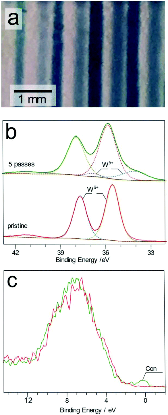 | ||
| Fig. 5 Photograph of the plasma treated tracks on the WO3 surface produced after 1, 3, 4 and 5 passes (a) (note that the faint lines in between are shadows cast on the supporting substrate). High resolution W 4f XPS spectra from the treated and pristine WO3 surfaces (b). Valence band spectra of the same samples (c). | ||
The high resolution W 4f XPS spectrum of the treated and untreated spots displayed two main features attributed to the W 4f7/2 and 4f5/2 states located at 35.5 and 37.8 eV for the pristine films, Fig. 5b.29 The low FWHM value of the 4f7/2 peak (0.99–1.02 eV) can be seen as an indicator of high crystallinity of the films.30 In the plasma treated region, the main W6+ 4f7/2 peak is shifted from 35.6 to 35.9 eV after 10 passes of the plasma jet. Furthermore, two additional peaks become discernible at 34.1 and 36.9 eV, assigned to W5+ species. Similar changes to the surface have also been reported after both Ar+ ion bombardment31 and electrochemical reduction of WO3 films.32
After 5 passes of the plasma jet, the relative atomic abundances of these two species are 79 and 21% for W6+ and W5+, respectively. The blue W5+ rich tracks were found to be stable under ambient air conditions for longer than seven days. The transparent WO3 film was fully recovered by annealing in air for 5 minutes at 250 °C. The O 1s spectrum for the treated and untreated WO3 surfaces (Fig. S7†) showed that two main peaks at 530.5 and 532.6 eV are present, attributed to oxygen in the WO3 lattice (Olat) and the surface adsorbed species (Oads). Upon treatment, a third peak (Odef) is detected in the deconvoluted spectrum, situated at 531.2 eV. This peak is attributed to oxygen present in the oxygen deficient regions of the WO3 lattice. A new peak (labelled as Con in Fig. 5c) near the Fermi level appears in the XPS valence band spectrum of the sample after plasma exposure. Formation of this conduction band has been attributed to the W 5d band in tungsten oxide.33 As shown in Fig. 4, W5+ is present alongside W6+ in this sample so that the residual 5d electrons originating in the W5+ centres appear in the previously empty conduction band of WO3.
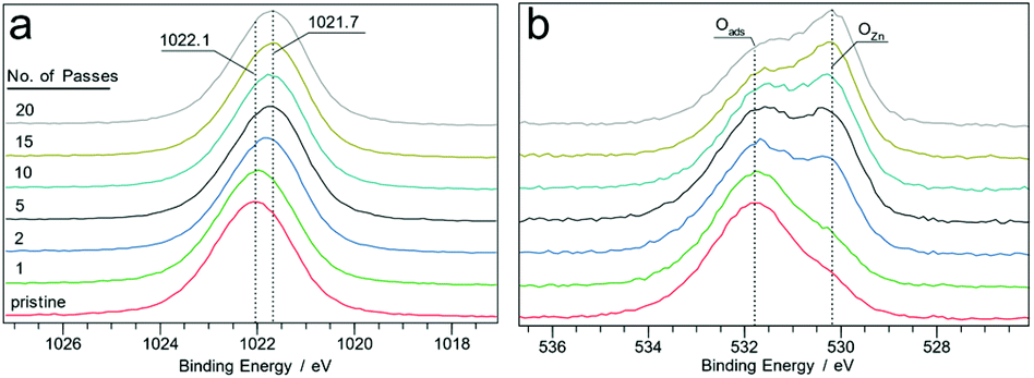
Plasma treated zinc oxide (ZnO) thin films also showed chemical reduction; however, in this case, the films remained transparent and colourless. High resolution Zn 2p XPS spectra obtained from the surfaces exposed to plasma for different durations showed a shift of approx. 0.4 eV from 1022.0 eV (for ZnO) to 1021.7 eV, as shown in Fig. 6a. There is also a concurrent decrease of the FWHM for the peaks from 1.89 eV to 1.78 eV after 20 passes of the plasma jet. The O 1s spectra obtained from the same points show two major components situated at 530.5 and 531.7 eV attributed to ZnO lattice oxygen (OZn) and adsorbed oxygen (Oads), as shown in Fig. 6b. With increasing number of plasma jet passes over the film, the Oads to OZn ratio is found to decrease, a change which was also observed for vacuum annealed ZnO films by Li et al.34 Also a steady decrease in the OZn/Zn atomic ratio of the film surface is found, which drops from 1.2 in the pristine surface to 0.7 after 20 passes, indicating that the plasma treated regions of the film were oxygen deficient. Despite evident oxygen deficiency, the Zn LMM Auger electron spectra (Fig. S8†) obtained from the treated surface do not show characteristic peaks arising from metallic zinc, suggesting that the plasma reduction of ZnO does not yield appreciable amounts of metallic Zn (unlike SnO2 and Cu2O).
 | ||
| Fig. 6 Zn 2p XPS spectra of the film surface at different numbers of plasma jet passes (a). The corresponding O 1s XPS spectra (b). | ||
Conclusions
Herein, we unambiguously demonstrate that a hydrogen doped helium atmospheric plasma jet was able to change the redox state of thin films of metal oxides. Fig. 7 shows a plot of the relative abundances of different redox states as determined by XPS for the oxides tested. Copper oxide was converted into a significant amount of zero valence metal. In fact, after only five passes of the plasma jet over the substrate, amounting to 5 s residence time on any part of the surface, the surface composition was found to be composed of 39% Cu(OH)2/CuO, 45% Cu and 16% Cu2O, as shown in Fig. 7a. Relative atomic concentrations of oxygen and copper on the surface agree with these findings, exhibiting a significant drop in the O/Cu atomic ratio from 1.3 to 0.8 after the plasma treatment. However, as discussed above, it is likely that the actual percentage of metallic copper is higher, as the XPS analysis is dominated by the top few atomic layers from the air exposed surface.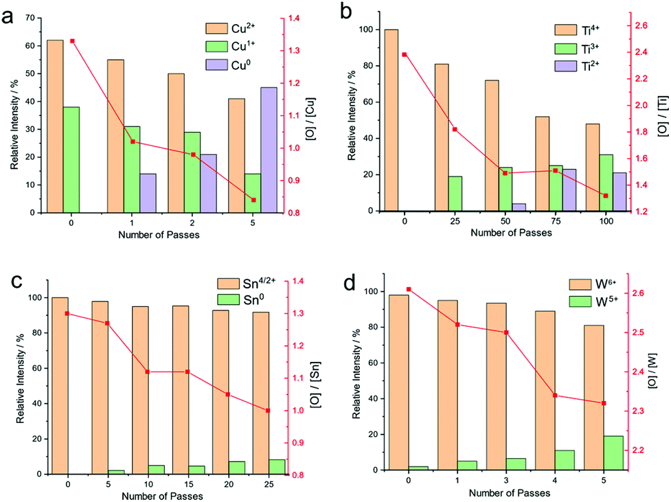 | ||
| Fig. 7 Bar graphs showing the relative % atom of different oxidation states for copper (a), titanium (b), tin (c) and tungsten (d) as determined by XPS analysis. The oxygen/metal atomic ratio of the film surface determined from XPS as a function of increasing plasma treatment duration is also shown. The error for bar graphs from the peak fitting procedure was 5–10%. | ||
Deconvolution of the XPS spectra for titanium dioxide treated with plasma show that the treated surface (Fig. 7b) exhibits a complicated peak structure composed of 3 peaks at 458.27, 456.77, and 455.15 eV attributed to Ti4+, Ti3+, and Ti2+ species, respectively. Ti4+, Ti3+ and Ti2+ proportions on the surface are calculated to be 46, 38 and 16%, respectively, after 100 passes of the plasma jet. This corresponds to a residence time of the plasma jet on any part of the track of approximately 1 min 40 s. This is an unprecedented level of redox conversion not seen in any other technique, particularly with such low power input.
Tin and tungsten oxides show a significant change in the oxide due to the direct action of the plasma on the surface, as summarized in Fig. 7c and d. In the case of tin, the change was to metallic tin, which was detectable after 25 passes, whereas with tungsten, only W5+ was detected by XPS. Similarly, the Odef+lat/W ratio on the surface calculated for the pristine and 5 passes-treated surface decreases from 2.6 to 2.3 upon treatment, indicating an oxygen deficient surface.
The mechanism for this plasma mediated reduction is uncertain at this point, an area we are investigating now. We propose a hypothesis which involves both free electrons and hydrogen. We know from plasma exposure of copper oxide that hydrogen (radical or otherwise) was not necessary for the reduction process, but speeds up the reduction process.17 Therefore, the excited electrons (either plasma or secondary electrons) are key for the reduction process.
In summary, a hydrogen doped helium atmospheric plasma jet can reduce metal oxides. Copper and tin oxides show complete reduction to zero valence metal; titanium, tungsten and zinc oxides form mixed oxides when exposed to the plasma. The reducing power of a micrometer sized atmospheric pressure plasma jet has been unambiguously demonstrated for several oxide surfaces. Assuming all the energy in the plasma is supplied to the surfaces, with no losses due to heating of the working gas; the peak and average power density is 6.3 and 0.9 W mm−2, respectively. This very small power input required to reduce quite stable oxides implies that the energy dissipation to affect the reduction is extremely efficient.
Experimental section
Plasma jet system
The plasma jet consisted of a powered tungsten electrode of 0.3 mm diameter placed centrally in a 40 mm long capillary tube of 1.4 mm inner diameter. One end of the capillary was pulled (Narishige, Japan, Model PE-21) to 0.5 mm diameter to serve as the plasma nozzle. The capillary was mounted in a larger borosilicate glass tube (20 mm O.D.) through a rubber septum with the nozzle end facing outwards. This glass tube was attached to the gas inlet. The jet used in this work produces dielectric barrier discharge plasma. The substrate serves as the dielectric barrier between the ground and the powered electrode. The powered electrode was connected to a 13.56 MHz RF generator via a matching network (Coaxial Power, UK). The driving voltage was pulse width modulated (PWM) using a square wave signal with a modulation frequency of 20 kHz (Tabor Electronics); see Table S1.† A schematic of the setup and the photo of the plasma jet are shown in Fig. 8. Plasma drive voltages were measured using a custom-built capacitively coupled voltage probe calibrated to −91 dB attenuation with a precision impedance analyzer (Agilent 4294A). The plasma current was measured via a clamp current probe placed around the cable attached to the powered electrode (Tektronix TCP202A). All waveforms were digitized and recorded using a digital phosphor oscilloscope (Tektronix DPO5000). The power delivered to the plasma during a single pulse was calculated by subtracting the power dissipated in the electrode in the plasma off state from the power dissipated in the plasma on state, obtained via integration of the measured voltage and current traces. The peak power during a plasma pulse was found to be 5 W leading to an average power measure of 0.7 W. This value is in agreement with the temperature of the working gas as it exits the jet nozzle (Table S1†).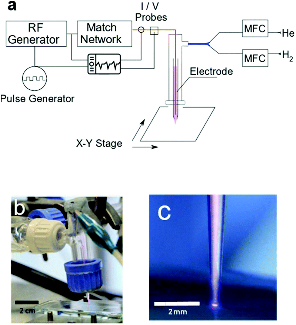 | ||
| Fig. 8 Schematic of the plasma jet setup (a). Photographs of the plasma jet over a glass substrate (b and c). | ||
Helium gas (CP Grade, BOC, UK) was mixed with 5% H2 gas (BOC, UK) with the aid of two mass flow controllers (Brooks Instruments, USA). This gas mixture, with a total flow rate of 0.2 l min−1, passes through the capillary where it is ignited and ejected from the nozzle forming a plasma jet. The metal oxide film coated samples were placed on a 2-axis motorized positioning stage beneath the plasma jet, 0.5 mm below the nozzle. For metal oxide sample preparation, please see the ESI.† The samples were constantly moved back and forth for a distance of 5 mm during the treatment period at a speed of 1 mm s−1 to create ‘tracks’ of treated regions on the film surface. The number of passes of the plasma jet over the surface was varied to probe the effect of plasma exposure time on the composition of the metal oxide films. The surface temperature of the substrates was measured using an infrared thermometer (Fluke, USA).
Optical emission spectra from the plasma jet were recorded using a fibre coupled UV-Vis optical emission spectrometer (HR-4000, Ocean Optics). The spectrum was found to be complex with major contributions from neutral and ionized molecular nitrogen entrained in the plasma plume. The major atomic emission lines were the hydrogen Hα line (656 nm) and He+ lines (688 and 728 nm); see Fig. S8.†
Surface characterization
A Thermo K-Alpha photoelectron spectroscopy system equipped with a monochromatic Al-Kα (1486.6 eV) X-ray source was used for XPS and Auger spectra acquisition. The spectra were collected from a spot of 50 μm diameter on the sample surface, at a pass energy of 50 eV. All samples were washed with D.I. water prior to XPS spectra collection, and no ion beam sputtering was used to further clean the surfaces to avoid damage to the film surface. Curve fitting was used for deconvolution of high resolution spectra using Voigt line shapes and Shirley background functions. Quantitative estimation of elemental composition was carried out by using Scofield's relative sensitivity factors for the relevant species.Renishaw inVia confocal Raman microscope with an unpolarized 532 nm argon ion laser excitation source was used for the characterization of the films. Raman spectra were obtained from an area of approximately 10 μm diameter with a 100× objective. The spectra were recorded in the 140 cm−1 to 1000 cm−1 Raman shift range at ambient temperature.
Scanning electron micrographs were obtained with a JEOL JSM 6701F SEM at an accelerating voltage of 10 kV with samples placed perpendicularly to the electron gun. The samples were cleaned by washing in distilled water followed by acetone.
Conflicts of interest
There are no conflicts to declare.Acknowledgements
The authors would like to thank Dr Steve Firth for the assistance with SEM. MES thanks the EPSRC for the PhD studentship.Notes and references
- (a) K. Ostrikov, J. Phys. D: Appl. Phys., 2011, 44, 17 Search PubMed; (b) U. Cvelbar, J. L. Walsh, M. Cernak, H. W. de Vries, S. Reuter, T. Belmonte, C. Corbella, C. Miron, N. Hojnik, A. Jurov, H. Puliyalil, M. Gorjanc, S. Portal, R. Laurita, V. Colombo, J. Schafer, A. Nikiforov, M. Modic, O. Kylian, M. Polak, C. Labay, J. M. Canal, C. Canal, M. Gherardi, K. Bazaka, P. Sonar, K. K. Ostrikov, D. Cameron, S. Thomas and K. D. Weltmann, Plasma Processes Polym., 2019, 16, 37 Search PubMed.
- T. Nozaki and K. Okazaki, Green Process. Synth., 2012, 1, 517 CAS.
- (a) S. Bornholdt, M. Wolter and H. Kersten, Eur. Phys. J. D, 2010, 60, 653 CrossRef CAS; (b) R. Foest, E. Kindel, H. Lange, A. Ohl, M. Stieber and K. D. Weltmann, Contrib. Plasma Phys., 2007, 47, 119 CrossRef CAS.
- (a) S. K. Lee, P. K. J. Robertson, A. Mills, D. McStay, N. Elliott and D. McPhail, Appl. Catal., B, 2003, 44, 173 CrossRef CAS; (b) X. B. Chen, L. Liu, P. Y. Yu and S. S. Mao, Science, 2011, 331, 746 CrossRef CAS PubMed; (c) X. B. Chen, L. Liu and F. Q. Huang, Chem. Soc. Rev., 2015, 44, 1861 RSC.
- (a) D. J. Caruana and S. P. McCormack, Electrochem. Commun., 2002, 4, 780 CrossRef CAS; (b) E. Hadzifejzovic, A. Elahi and D. J. Caruana, Thin Solid Films, 2012, 520, 5254 CrossRef CAS; (c) E. Hadzifejzovic, J. A. S. Galiani and D. J. Caruana, Phys. Chem. Chem. Phys., 2006, 8, 2797 RSC; (d) A. Elahi, T. Fowowe and D. J. Caruana, Angew. Chem., Int. Ed., 2012, 51, 6350 CrossRef CAS PubMed; (e) A. Elahi and D. J. Caruana, Phys. Chem. Chem. Phys., 2013, 15, 1108 RSC.
- (a) E. P. Stuckert and E. R. Fisher, Sens. Actuators, B, 2015, 208, 379 CrossRef CAS; (b) E. P. Stuckert, C. J. Miller and E. R. Fisher, J. Vac. Sci. Technol., B: Nanotechnol. Microelectron.: Mater., Process., Meas., Phenom., 2017, 35, 10 Search PubMed; (c) H. Schade, Z. E. Smith, J. H. Thomas and A. Catalano, Thin Solid Films, 1984, 117, 149 CrossRef CAS.
- (a) Y. Yan, M. Y. Han, A. Konkin, T. Koppe, D. Wang, T. Andreu, G. Chen, U. Vetter, J. R. Morante and P. Schaaf, J. Mater. Chem. A, 2014, 2, 12708 RSC; (b) Z. Wang, C. Y. Yang, T. Q. Lin, H. Yin, P. Chen, D. Y. Wan, F. F. Xu, F. Q. Huang, J. H. Lin, X. M. Xie and M. H. Jiang, Adv. Funct. Mater., 2013, 23, 5444 CrossRef CAS.
- Y. Sawada, N. Taguchi and K. Tachibana, Jpn. J. Appl. Phys., Part 1, 1999, 38, 6506 CrossRef CAS.
- K. C. Sabat, R. K. Paramguru and B. K. Mishra, Plasma Chem. Plasma Process., 2016, 36, 1111 CrossRef CAS.
- H. Inui, K. Takeda, H. Kondo, K. Ishikawa, M. Sekine, H. Kano, N. Yoshida and M. Hori, Appl. Phys. Express, 2010, 3, 126101 CrossRef.
- (a) L. Di, Z. Li, B. Lee and D.-W. Park, Int. J. Hydrogen Energy, 2017, 42, 11372 CrossRef CAS; (b) L. Di, Z. Li, X. Zhang, H. Wang and Z. Fan, Catal. Today, 2019, 337, 55 CrossRef CAS.
- L. B. Di, X. L. Zhang, B. Lee, P. Lu, W. S. Ahn and D. W. Park, Plasma Chem. Plasma Process., 2017, 37, 1535 CrossRef CAS.
- L. Di, J. Zhang and X. Zhang, Plasma Processes Polym., 2018, 15, 1700234 CrossRef.
- E. Hadzifejzovic, J. Stankovic, S. Firth, P. F. McMillan and D. J. Caruana, Phys. Chem. Chem. Phys., 2007, 9, 5335 RSC.
- (a) C. Richmonds, M. Witzke, B. Bartling, S. W. Lee, J. Wainright, C. C. Liu and R. M. Sankaran, J. Am. Chem. Soc., 2011, 133, 17582 CrossRef CAS PubMed; (b) S. A. Meiss, M. Rohnke, F. Rettig, R. Moos and J. Janek, Contrib. Plasma Phys., 2008, 48, 473 CrossRef CAS; (c) S. A. Meiss, M. Rohnke, L. Kienle, S. Z. El Abedin, F. Endres and J. Janek, ChemPhysChem, 2007, 8, 50 CrossRef CAS PubMed; (d) M. Brettholle, O. Hofft, L. Klarhofer, S. Mathes, W. Maus-Friedrichs, S. Z. El Abedin, S. Krischok, J. Janek and F. Endres, Phys. Chem. Chem. Phys., 2010, 12, 1750 RSC.
- R. Hawtof, S. Ghosh, E. Guarr, C. Y. Xu, R. M. Sankaran and J. N. Renner, Sci. Adv., 2019, 5, 1 Search PubMed.
- M. E. Sener and D. J. Caruana, Electrochem. Commun., 2018, 95, 38 CrossRef CAS.
- S. W. Lee, D. Liang, X. P. A. Gao and R. M. Sankaran, Adv. Funct. Mater., 2011, 21, 2155 CrossRef CAS.
- Y. Sui, Y. Dai, C. C. Liu, R. M. Sankaran and C. A. Zorman, Adv. Mater. Technol., 2019, 4, 1900119 CrossRef CAS.
- M. C. Biesinger, Surf. Interface Anal., 2017, 49, 1325 CrossRef CAS.
- M. C. Biesinger, L. W. M. Lau, A. R. Gerson and R. S. C. Smart, Appl. Surf. Sci., 2010, 257, 887 CrossRef CAS.
- L. L. Wu, L. K. Tsui, N. Swami and G. Zangari, J. Phys. Chem. C, 2010, 114, 11551 CrossRef CAS.
- N. Pauly, S. Tougaard and F. Yubero, Surf. Sci., 2014, 630, 294 CrossRef CAS.
- U. Diebold and T. E. Madey, Surf. Sci. Spectra, 1996, 4, 227 CrossRef CAS.
- M. Mehta, N. Kodan, S. Kumar, A. Kaushal, L. Mayrhofer, M. Walter, M. Moseler, A. Dey, S. Krishnamurthy, S. Basu and A. P. Singh, J. Mater. Chem. A, 2016, 4, 2670 RSC.
- M. A. Stranick and A. Moskwa, Surf. Sci. Spectra, 1993, 2, 50 CrossRef CAS.
- M. A. Stranick and A. Moskwa, Surf. Sci. Spectra, 1993, 2, 45 CrossRef CAS.
- J. H. Thomas, Appl. Phys. Lett., 1983, 42, 794 CrossRef CAS.
- F. Y. Xie, L. Gong, X. Liu, Y. T. Tao, W. H. Zhang, S. H. Chen, H. Meng and J. Chen, J. Electron Spectrosc. Relat. Phenom., 2012, 185, 112–118 CrossRef CAS.
- J. Wang, R. S. Chen, L. Xiang and S. Komarneni, Ceram. Int., 2018, 44, 7357 CrossRef CAS.
- F. Y. Xie, L. Gong, X. Liu, Y. T. Tao, W. H. Zhang, S. H. Chen, H. Meng and J. Chen, J. Electron Spectrosc. Relat. Phenom., 2012, 185, 112 CrossRef CAS.
- N. Xu, M. Sun, Y. W. Cao, J. N. Yao and E. G. Wang, Appl. Surf. Sci., 2000, 157, 81 CrossRef CAS.
- B. A. Deangelis and M. Schiavello, J. Solid State Chem., 1977, 21, 67 CrossRef CAS.
- X. Y. Li, Y. L. Wang, W. F. Liu, G. S. Jiang and C. F. Zhu, Mater. Lett., 2012, 85, 25 CrossRef CAS.
Footnote |
| † Electronic supplementary information (ESI) available. See DOI: 10.1039/d0gc00080a |
| This journal is © The Royal Society of Chemistry 2020 |