 Open Access Article
 This Open Access Article is licensed under a
 Creative Commons Attribution 3.0 Unported Licence
Raman spectroscopy of GaSe and InSe post-transition metal chalcogenides layers†
Maciej R.
Molas
 a,
Anastasia V.
Tyurnina
bcd,
Viktor
Zólyomi
bc,
Anna K.
Ott
e,
Daniel J.
Terry
bc,
Matthew J.
Hamer
bc,
Celal
Yelgel
c,
Adam
Babiński
a,
Albert G.
Nasibulin
d,
Andrea C.
Ferrari
*e,
Vladimir I.
Fal’ko
bcf and
Roman
Gorbachev
bcf
a,
Anastasia V.
Tyurnina
bcd,
Viktor
Zólyomi
bc,
Anna K.
Ott
e,
Daniel J.
Terry
bc,
Matthew J.
Hamer
bc,
Celal
Yelgel
c,
Adam
Babiński
a,
Albert G.
Nasibulin
d,
Andrea C.
Ferrari
*e,
Vladimir I.
Fal’ko
bcf and
Roman
Gorbachev
bcf
aInstitute of Experimental Physics, Faculty of Physics, University of Warsaw, Pasteura 5, 02-093 Warszawa, Poland
bSchool of Physics and Astronomy, University of Manchester, Oxford Road, M13 9PL, UK
cNational Graphene Institute, University of Manchester, Booth St E, Manchester, M13 9PL, UK
dSkolkovo Institute of Science and Technology, Nobel St. 3, 143026 Moscow, Russia
eCambridge Graphene Centre, University of Cambridge, 9 JJ Thomson Avenue, Cambridge, CB3 0FA, UK. E-mail: acf26@eng.cam.ac.uk
fHenry Royce Institute, University of Manchester, Oxford Road, Manchester, M13 9PL, UK
First published on 16th March 2020
Abstract
III–VI post-transition metal chalcogenides (InSe and GaSe) are a new class of layered semiconductors, which feature a strong variation of size and type of their band gaps as a function of number of layers (N). Here, we investigate exfoliated layers of InSe and GaSe ranging from bulk crystals down to monolayer, encapsulated in hexagonal boron nitride, using Raman spectroscopy. We present the N-dependence of both intralayer vibrations within each atomic layer, as well as of the interlayer shear and layer breathing modes. A linear chain model can be used to describe the evolution of the peak positions as a function of N, consistent with first principles calculations.
Introduction
Layered materials (LMs) are at the centre of an ever-increasing research effort spanning across a multitude of scientific disciplines.1 In addition to widely popular semiconducting transition metal dichalcogenides (TMDs), such as MoS2, MoSe2, MoTe2, WS2 and WSe2, a new class of LMs, semiconducting post-transition metal chalcogenides (PTMCs), are increasingly studied.2–6 These materials feature a large variation of the optical bandgap with number of layers, N: from 1.25 eV in bulk to 2.8 eV in monolayer (1L) InSe3,4,6 and from 2.0 eV (bulk) to 2.4 eV (bilayer, 2L) in GaSe.5 Furthermore, the band-gap evolves from being quasi-direct for 1L to direct in bulk. These materials also feature outstanding electronic transport properties, e.g. in InSe mobilities reach up to 103 cm2 V−1 s−1 and 104 cm2 V−1 s−1 at room and liquid-helium temperatures4, as well as one-dimensional quantization of electrons by electrostatic gating,7 and unusual photoluminescence, polarized primarily out of the basal plane.6 They can be combined into PTMC/PTMC or PTMC/TMD layered materials heterostructures (LMHs), with type-II band alignment, allowing direct optical transitions in reciprocal space,8 and offering an even larger selection of emission energies,5 with potential for novel optoelectronic applications in a broad spectral range, from far infra-red to violet.GaSe and InSe crystals are anisotropic LMs comprising covalently bonded layers stacked together by van der Waals forces. Each layer consists of four atomic planes (Se–Ga–Ga–Se or Se–In–In–Se) arranged in a hexagonal atomic lattice, Fig. 1a and b. In bulk, these layers can be stacked in a different orders: a hexagonal β-structure belonging to the D46h space group, a hexagonal ε-structure belonging to the D13h space group or a rhombohedral γ-structure belonging to the DS3v space group.9 However, the most commonly found polytypes are ε-GaSe, with a unit cell containing 8 atoms and two layers thick,5 and γ-InSe, with a unit cell extending over 3 layers, containing 12 atoms.6
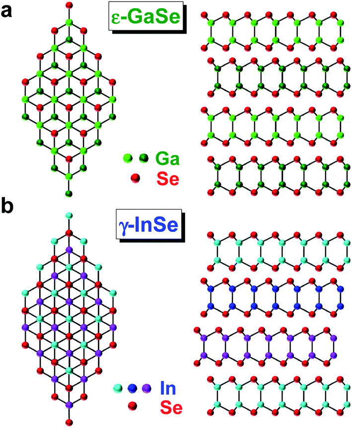 | ||
| Fig. 1 Atomic structure and stacking order of (a) ε-GaSe and (b) γ-InSe. | ||
Raman spectroscopy is the prime non-destructive characterization tool for graphene and LMs.10–13 In LMs there are 2 fundamentally different sets of Raman modes. Those coming from the relative motion of atoms within each layer, usually found at high frequencies,10,11 and those due to relative motions of the atomic planes themselves, either parallel to each other (C modes)12 or perpendicular (layer breathing modes, LBMs).13 For the latter the experimental results can be interpreted using with a simple linear chain model (LCM), whereby each plane is considered linked to the next one by a spring corresponding to an interlayer force constant per unit area (parallel or perpendicular to the planes for the two types of motion).12,13
So far, Raman characterization of PTMCs has been reported on few-layers thick crystals.14–18 Due to low signal-to-noise ratio and strong degradation occurring in ambient conditions,19 the thinnest PTMCs have not been investigated properly: background noise or incomplete spectra were reported, containing only one prominent Raman feature for 1L and 2L samples.14–18
Here, we present a Raman study of high crystalline quality InSe and GaSe flakes prepared by mechanical exfoliation, with thicknesses varying from bulk to 1L, encapsulated in hexagonal boron nitride (hBN) in an inert argon environment. We observe the thickness-dependent evolution of both intralayer vibrations as well as C and LB modes, and compare the experimental results with first principles calculations. We demonstrate that Raman spectroscopy can be used to estimate N of PTMCs, in agreement with the LCM.
Results and discussion
GaSe and InSe samples are prepared using a micromanipulation setup placed inside an Ar filled glovebox to prevent the air-induced degradation. Bulk PTMC crystals are mechanically exfoliated onto a 200 nm layer of poly-(propylene carbonate) (PPC), spin coated onto a Si wafer and identified using optical microscopy.20 Selected PTMC flakes are then picked up with thin hBN layers residing on a polymer membrane using a dry peel transfer technique.19 The resulting PTMC/hBN stack is then transferred onto another hBN crystal exfoliated onto a Si/SiO2 substrate, to achieve full encapsulation. The verification of the PTMC thicknesses is performed using atomic force microscopy (AFM).Raman measurements are carried out in backscattered geometry at room temperature using Renishaw, Horiba LabRam HR Evolution, Horiba XploRa and Horiba FHR1000 systems equipped with interference or Bragg grating filters, with a cut-off at 5 cm−1. The Raman spectra are taken at 633 nm (1.96 eV), 532 nm (2.33 eV), 515 nm (2.41 eV), 488 nm (2.54 eV), and 457 nm (2.71 eV). The laser is focused by a 100× objective. The laser power on the sample is kept at ∼150 μW during all measurements, to avoid damage and local heating. The collected signal is dispersed with 1800 and 2400 grooves mm−1 gratings and detected with a CCD camera. For each measurement, the spectrum from an area near each studied layer is subtracted, to remove the Si substrate background. The background spectra are also used for calibration of the data from different setups, using the Si Raman mode at 520.7 cm−1.21
Fig. 2 plots the polarization-resolved Raman spectra of three layer (3L) GaSe and InSe, accompanied by the corresponding atomic displacement of the phonon modes. 3L GaSe has two out-of-plane phonon modes,  at ∼135 cm−1 and
  at ∼308 cm−1, and one in-plane E′′(2) mode at ∼214 cm−1. 3L InSe has 3 out-of-plane modes:
  at ∼115 cm−1,
  at ∼200 cm−1 and
  at ∼228 cm−1, and one in-plane E′′(2) mode at ∼178 cm−1. The peaks are classified according to their irreducible representation in the symmetry group in the 1L phase D3h, and additionally numbered due to their increased Raman shift. This notation is consistent with earlier works on bulk ε-GaSe, γ-InSe.22–25
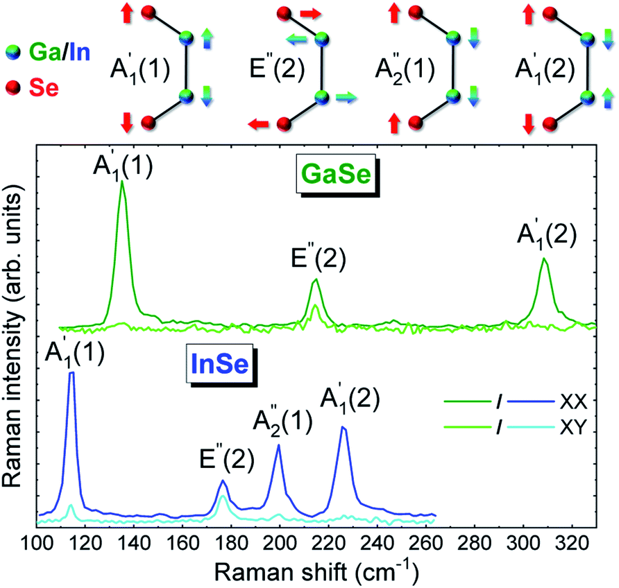 | ||
| Fig. 2 Atomic displacements of phonon modes and polarization-resolved 514.5 nm Raman spectra of 3L GaSe (green/bright green) and InSe (blue/bright blue) in XX/XY configurations. | ||
To confirm their symmetries, the Raman spectra are recorded at 488 nm for 2 polarizations: parallel – XX and cross-polarized – XY. For both materials, all peaks are observed in XX, while only E′′(2) modes are seen in XY, as expected due to the rotational symmetry in these crystals, which implies that A-type modes are only active in parallel polarization, while E-type modes are observable in both (see ESI† for details).
In order to reveal the evolution of the Raman spectra with N, crystals with multiple terraces with lateral size >1 μm are studied. The unpolarized Raman spectra, presented in Fig. 3a and b, show the optical phonon modes down to 1L.
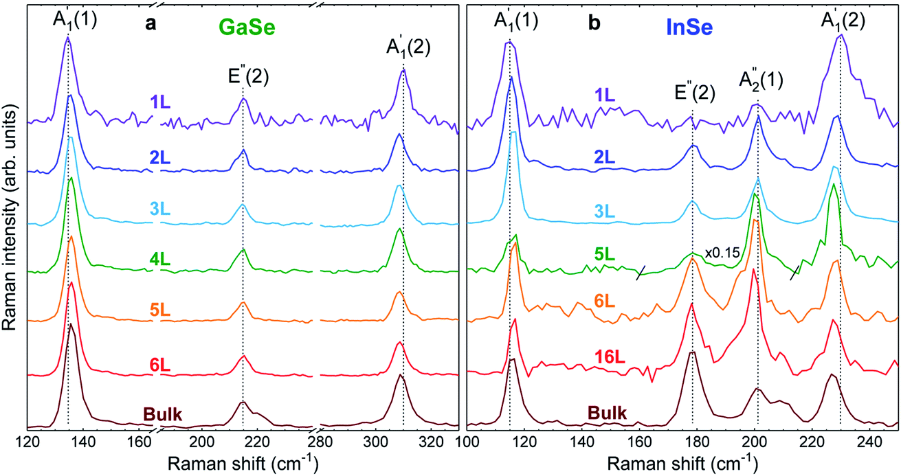 | ||
| Fig. 3 Unpolarized Raman spectra as a function of N for (a) GaSe and (b) InSe measured at 488 nm. Dashed lines show peak positions for 1L. | ||
For GaSe,  and
and  red- and blue-shift, respectively, with decreasing N, while E′′(2) is barely affected by N. For bulk, a double peak is observed, comprising E′′(2) at ∼211 cm−1 and E′(2) at ∼216 cm−1, consistent with first principles calculations (see ESI†), and previous Raman studies of bulk crystals.22,23 The E′(2) mode corresponds to an in-plane phonon, where Ga or Se atoms vibrate in-phase, while an out-of-phase vibration occurs between Ga and Se pairs.
For InSe, Fig. 3b, we observe a similar red- and blue-shift of  and
and  with decreasing N, and no significant shift of E′′(2), while
  blueshifts like
  . For 16L and bulk, an additional peak is seen at ∼210 cm−1, visible under XY polarization, suggesting it to be an E-type vibration. As for ref. 26–28, we assign it to an E′(2) mode, similar to GaSe bulk. The observation of
  in the Raman spectrum of InSe bulk was previously ascribed to resonance with the B excitonic transition.25Ref. 3 showed that the B energy is affected by N, changing from ∼2.4 eV in bulk to ∼2.9 eV for 1L. For a constant excitation of 2.54 eV as used in Fig. 3, the resonance is strongest for intermediate thicknesses, with the largest
  intensity for 5L, Fig. 3b.
The evolution of peaks' positions with N, extracted using Lorentzian fits, for both materials is shown in Fig. 4a and b. Previous publications reported only one phonon mode in thin crystals down to 1L, i.e. for GaSe15 and
  for InSe,16 likely due to the lack of encapsulation, leading to crystal degradation.29 The reported N evolution of
  in GaSe15 is opposite (a redshift with decreasing N) to our observations, which may be due to an overlap of the
  mode with Si modes ∼300 cm−1 in ref. 20. In InSe, a similar redshift of
  was previously reportedobserved down to 2L.16 However, the Raman signal of 1L was not detected, and only
  was visible in 2L.
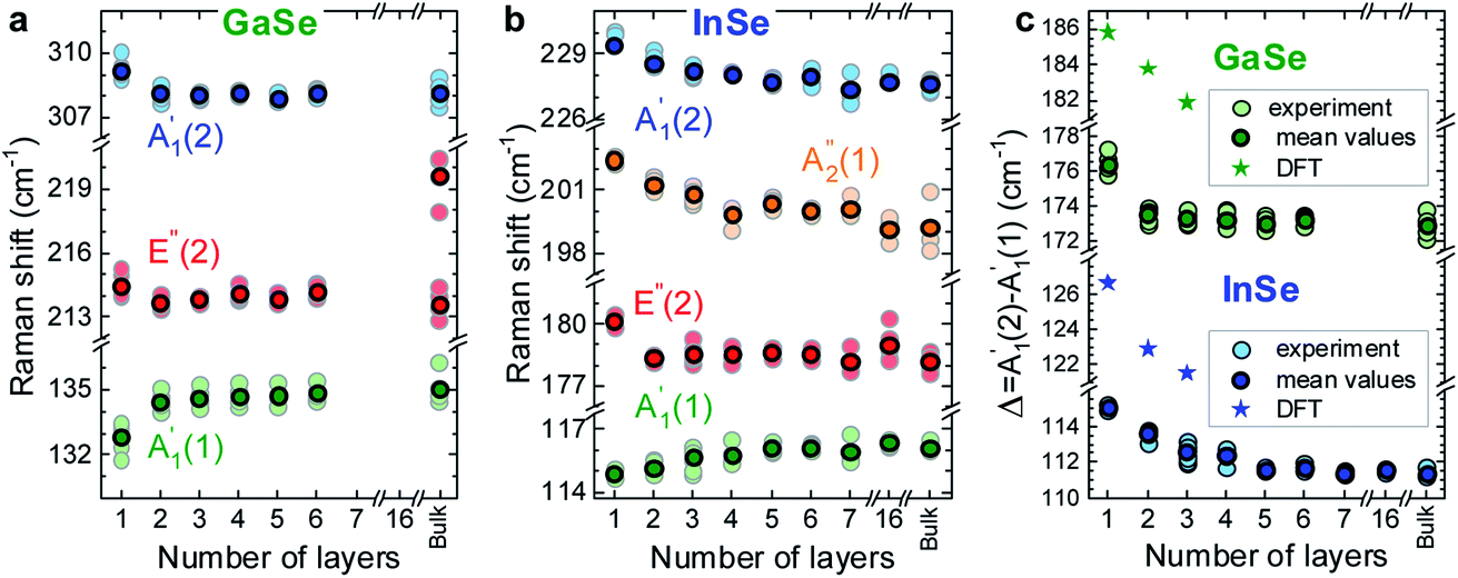 | ||
Fig. 4
N-dependent Raman shifts for (a) GaSe and (b) InSe. (c) N dependence of 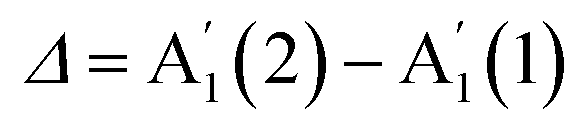 . DFT calculations are indicated by star symbols. The dark color symbols correspond to mean values for the dataset shown in light colors measured at 633, 533, 514.5, 488 and 457 nm. . DFT calculations are indicated by star symbols. The dark color symbols correspond to mean values for the dataset shown in light colors measured at 633, 533, 514.5, 488 and 457 nm. | ||
We further investigate the N dependence of the difference in peaks' positions between  and
and  , i.e.
 . According to our DFT calculations presented in the ESI,† a gradual rise in Δ with decreasing N is predicted for both materials, Fig. 4c. This matches our experimental results for InSe, where Δ is gradually increasing from 5L to 1L, with a total blueshift ∼3.5 cm−1. A more abrupt change is observed in GaSe, where Δ only changes noticeably in 1L by ∼3 cm−1. Δ in both materials is enough to be used for assessing N in few layer (FL) In Se and 1L-GaSe, similar to what done for TMDs.29,30
Fig. 5 plots the low frequency Raman spectra of InSe and GaSe flakes. Fig. 5a and b show 3 types of Raman peaks for both materials. Two of them are due to the vibrations in the GaSe and InSe layers, while the peak at ∼52 cm−1, indicated by *, is the C peak of the encapsulating hBN.
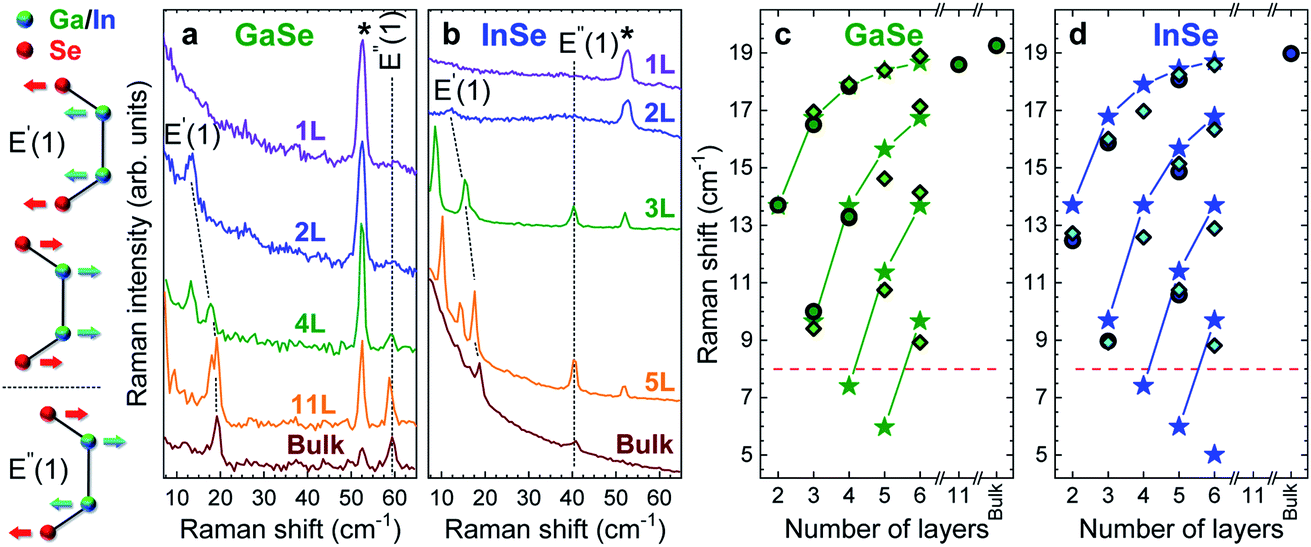 | ||
| Fig. 5 Atomic displacements of phonon modes and unpolarized 514.5 nm low-frequency Raman spectra as a function of N for (a) GaSe and (b) InSe. Dashed lines are guides to the eye. (c and d) N dependence of C modes of (c) GaSe and (d) InSe. Circles and diamonds denote experimental results. Stars are DFT calculations. Dashed red horizontal lines represent the minimal Raman shift ∼8 cm−1 detectable in our experiments. | ||
The evolution of C and LB modes can be described using a LCM, where the layers are represented as one mass connected to the next layer by a spring with a coupling constant. Pos(C) and Pos(LBM) can then be written as:11–13
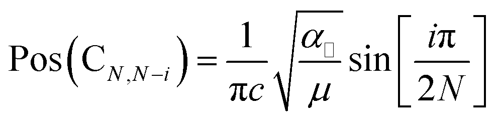 | (1) |
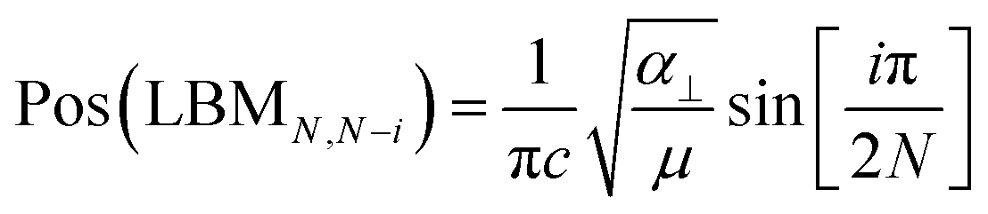 | (2) |
We also use DFT within the local density approximation (LDA) to calculate the vibrational frequencies, as detailed in the ESI.† To compute the C and LBM frequencies, we rely on the frozen phonon approximation to calculate the corresponding force constant between neighbouring layers. The interlayer force constant remains the same, within 1%, when increasing N from 2 to 3. Therefore, the LCM approach can be applied to C modes under the assumption that independent force constants describe the coupling between neighbouring layers. Such an approximation was previously applied to ε-GaSe.31 We obtain the interlayer force constants: for C modes, KGaSe = 102 meV Å−2 and KInSe = 134 meV Å−2; for LBMs, KGaSe = 323 meV Å−2 and KInSe = 401 meV Å−2.
In our experiments, we only observe C modes. Fig. 5c and d plot experimental and calculated Pos(C).34 The results are in good agreement, both concerning frequencies and number of branches for a given N. By fitting the measured Pos(C) as function of N with eqn (1), we get α‖ ∼ 14.4 × 10¹⁸ N m−3 for InSe and ∼13.3 × 10¹⁸ N m−3 for GaSe. We use the experimental values for the lattice constants aexpInSe = 4.002 Å (ref. 32) and aexpGaSe = 3.755 Å (ref. 33) to extract the unit area. Using the LDA lattice parameters aGaSe = 3.6678 Å and aInSe = 3.9103 Å and computing the unit cell areas, we can extract α‖ from the theoretical interlayer force constants K for InSe and GaSe by dividing K by the unit cell area. We get 16 × 1018 N m−3 for InSe and 14 × 1018 N m−3 for GaSe, in good agreement with the experimentally determined values.
Conclusions
We performed a Raman spectroscopic investigation of InSe and GaSe flakes of varying number of layers from bulk down to a monolayer, for samples encapsulated in hBN. We determined the thickness-dependent evolution of both intralayer and interlayer modes, and compared the results with first principles calculations. We confirmed that Raman spectroscopy can be used to estimate the number of layers of PTMCs.Conflicts of interest
There are no conflicts to declare.Acknowledgements
We acknowledge support from the National Science Centre, Poland (grants no. 2017/24/C/ST3/00119, 2017/27/B/ST3/00205), EPSRC ARCHER RAP grant (e547), EU Graphene Flagship and Quantum Technology Flagships, The Scientific and Technological Research Council of Turkey (TUBITAK) through BIDEB-2219 programme (2018-1), EPSRC CDT Graphene-NOWNANO and Graphene Technology, EPSRC Doctoral Prize Fellowship, Royal Society Research Fellowship, Samsung Advanced Institute of Technology (SAIT), ERC Grant Hetero2D, EPSRC Grants EP/K01711X/1, EP/K017144/1, EP/N010345/1 and EP/L016057/1.References
- A. C. Ferrari, et al. , Nanoscale, 2015, 7, 4598 RSC.
- W. Choi, N. Choudhary, G. H. Han, J. Park, D. Akinwande and Y. H. Lee, Mater. Today, 2017, 20, 116 CrossRef CAS.
- G. W. Mudd, et al. , Sci. Rep., 2016, 6, 39619 CrossRef CAS PubMed.
- D. A. Bandurin, et al. , Nat. Nanotechnol., 2017, 12, 223 CrossRef CAS PubMed.
- D. J. Terry, et al. , 2D Materials, 2018, 5, 041009 CrossRef CAS.
- M. J. Hamer, et al. , ACS Nano, 2019, 13, 2136 CAS.
- M. Hamer, et al. , Nano Lett., 2018, 18, 3950 CrossRef CAS PubMed.
- N. Ubrig, et al., 2019, arXiv:1912.10345.
- S. Jandl and C. Carlone, Solid State Commun., 1978, 25, 5 CrossRef CAS.
- A. C. Ferrari, et al. , Phys. Rev. Lett., 2006, 97, 187401 CrossRef CAS PubMed.
- A. C. Ferrari and D. M. Basko, Nat. Nanotechnol., 2013, 8, 235 CrossRef CAS PubMed.
- P. H. Tan, et al. , Nat. Mater., 2012, 11, 294 CrossRef CAS PubMed.
- X. Zhang, et al. , Phys. Rev. B: Condens. Matter Mater. Phys., 2013, 87, 115413 CrossRef.
- D. J. Late, et al. , Adv. Mater., 2012, 24, 3549 CrossRef CAS PubMed.
- D. J. Late, et al. , Adv. Funct. Mater., 2012, 22, 1894 CrossRef CAS.
- Z. Chen, K. Gacem, M. Boukhicha, J. Biscaras and A. Shukla, Nanotechnology, 2013, 24, 415708 CrossRef PubMed.
- L. Quan, et al. , J. Mater. Chem. C, 2015, 3, 11129 RSC.
- Y. Li, et al. , 2D Materials, 2018, 5, 021002 CrossRef.
- Y. Cao, et al. , Nano Lett., 2015, 15, 4914 CrossRef CAS PubMed.
- C. Casiraghi, et al. , Nano Lett., 2007, 7, 2711 CrossRef CAS PubMed.
- P. A. Temple and C. E. Hathaway, Phys. Rev. B: Solid State, 1973, 7, 3685 CrossRef CAS.
- N. Kuroda and Y. Nishina, Solid State Commun., 1980, 34, 481 CrossRef CAS.
- N. M. Gasanly, A. Aydınlı, H. Özkan and C. Kocabaş, Mater. Res. Bull., 2002, 37, 169 CrossRef CAS.
- R. M. Hoff, J. C. Irwin and R. M. A. Lieth, Can. J. Phys., 1975, 53, 1606 CrossRef CAS.
- N. Kuroda and Y. Nishina, Solid State Commun., 1978, 28, 439 CrossRef CAS.
- N. M. Gasanly, B. M. Yavadov, V. I. Tagirov and E. A. Vinogradov, Phys. Status Solidi B, 1978, 89, K43 CrossRef CAS.
- S. Ashokan, K. P. Jain, M. Balkanski and C. Julien, Phys. Rev. B: Condens. Matter Mater. Phys., 1991, 44, 11133 CrossRef CAS PubMed.
- I. H. Choi and P. Y. Yu, J. Appl. Phys., 2003, 93, 4673 CrossRef CAS.
- O. Del Pozo-Zamudio, et al., 2015, arXiv:1506.05619.
- C. Lee, et al. , ACS Nano, 2010, 4, 2695 CrossRef CAS PubMed.
- R. Longuinhos and J. Ribeiro-Soares, Phys. Chem. Chem. Phys., 2016, 18, 25401 RSC.
- J. Rigoult, A. Rimsky and A. Kuhn, Acta Crystallogr., Sect. B: Struct. Crystallogr. Cryst. Chem., 1980, 36, 916 CrossRef.
- F. Jellinek and H. Hahn, Z. Naturforsch., B, 1961, 16b, 713 CrossRef CAS.
- G. Pizzi, S. Milana, A. C. Ferrari, N. Marzari and M. Gibertini, 2020, arXiv:2011.14681.
Footnote |
| † Electronic supplementary information (ESI) available: S1: selection rules for E′ and E′′ phonons. S2: Γ-point frequencies in FL-GaSe and InSe. S3: resonance effects. See DOI: 10.1039/d0fd00007h |
| This journal is © The Royal Society of Chemistry 2021 |