 Open Access Article
 This Open Access Article is licensed under a Creative Commons Attribution-Non Commercial 3.0 Unported Licence
Photophysical properties of ball milled silicon nanostructures†
Ankit
Goyal
 *,
Menno
Demmenie
,
Chia-Ching
Huang
,
Peter
Schall
and
Katerina
Dohnalova
*,
Menno
Demmenie
,
Chia-Ching
Huang
,
Peter
Schall
and
Katerina
Dohnalova
University of Amsterdam, Institute of Physics, Science Park 904, 1098XH, Amsterdam, The Netherlands. E-mail: a.goyal@uva.nl
First published on 22nd October 2019
Abstract
Luminescent silicon nanocrystals (SiNCs) have attracted scientific interest for their potential use in LEDs, displays, lasers, photovoltaic spectral-shifting filters and for biomedical applications. A lot of efforts have been made to improve the radiative emission rate in SiNCs, mostly using quantum confinement, strain and ligands. Existing methods, however, are not easily upscalable, as they do not provide the high material yield required for industrial applications. Besides, the photoluminescence (PL) efficiency of SiNCs emitting in the visible spectral range also remains very low. Hence, there is a need to develop a low-cost method for high material yield of brightly emitting SiNCs. Theoretically, strain can be used alongside quantum confinement to modify the radiative emission rates and band-gaps. In view of that, high-energy ball milling is a method that can be used to produce large quantities of highly strained SiNCs. In this technique, balls with high kinetic energy collide with the walls of a chamber and other balls, crushing the particles in between, followed by welding, fracture and re-welding phenomena, reducing the particle size and increasing strains in the samples. In this study, we have used high-energy ball milling in an inert gas atmosphere to synthesize SiNCs and study their photophysical properties. The induced accumulation of high strain, quantum confinement and possibly also impurities in the SiNCs resulted in visible light spectrum PL at room temperature. This method is low cost and easily up-scalable to industrial scale.
Introduction
Unlike bulk Si, Si nanocrystals (SiNCs) are a promising material for applications in LEDs, lasers, displays and as spectral-shifting filters in photovoltaics etc., due to their increased emission rates and size-tunable band-gaps (see, e.g.1–3). Higher radiative emission rates and visible emission in the blue, green and red regions of the spectrum have been reported for various types of SiNCs.4–10 However, production methods of SiNCs with emission in the UV and visible spectral region (and the vast majority of the NIR emitting SiNCs) have not been capable of producing the high material yields required for commercial uses so far. Production of SiNCs with diameter below <10 nm is mostly performed by bottom-up syntheses – wet-chemical or from plasma.11–21 The important role of surface ligands often leads to limited spectral tunability.3 Hydrogen-, oxygen- and alkyl-capped SiNCs have been studied in detail.1,4,5,7,9,13–17,19,21,23–25 Hydrogen capped SiNCs show size-tunable emission, but are unstable and prone to oxidation upon exposure to air.1 Resulting oxide-capped SiNCs of diameters below 5 nm show either impurity-related red emission with slow rate23,26–28 or blue emission with fast rate29,30 and larger sized crystals (above ∼5 nm) show size-tunable emission in the near-IR range.22,31 Alkyl-terminated Si nanocrystals are considered very stable and resistant to oxidation, with luminescence in the visible range tunable by the ligands and size, showing direct bandgap-like radiative rates.13,19,21,23,32,33 Further means to manipulate the optical properties can be achieved using strain.34 Theoretical studies show that under tensile stress, it is possible to have direct bandgap-like Si nanocrystals.35,36 Despite these advances, silicon has yet to make its way to replace toxic and less abundant options to be used in aforesaid applications because of the low-yielding synthesis methods. There is an urgent need to have a method which can produce stable, non-toxic and highly emissive Si nanocrystals at industrial scale. In view of this, high-energy ball milling which was initially developed to mix different metals and then to produce alloys, might be used for this purpose. Recently, ball milling was used for the doping of V2O5 into nano-Si for Li-ion battery anodes.37 High-energy ball milling allows the synthesis of nanoparticles at kilogram scale in a short time.Here, we present SiNCs prepared using high-energy ball mill. This method is very high yielding and leads to SiNCs that emit in the blue-green region of the visible light spectrum. The occurrence of multiple phonon replicas in the photoluminescence (PL) spectra of the milled Si particles suggests the presence of localized emission centers, possibly impurities. We interpret the phenomena based on the presence of Si–O/Si–C bonds on the surface, as well as possible doping of the SiNC particles with iron and cobalt transition metal impurities, introduced by the milling environment. The results indicate a possible energy transfer from the excited SiNCs to the metallic impurities and/or to Si–O/Si–C bonds participating in the radiative processes. We do not see evidence of quantum confinement, since no shift in the PL peak position is observed upon reducing the nanoparticle size, even down to sizes of ∼5 nm. This suggest that impurities (and maybe also strain) play larger roles than quantum confinement. We perform structural and compositional analysis to determine the structure of the milled SiNCs and correlated it with the optical properties. However, more work, especially on in-depth elemental and structural analysis, is needed to support our claims.
Materials and methods
Silicon powder (99.999% purity) with an average particle size of <20 µm was purchased from Hongwu International Group Ltd, China. An unmilled Si sample was used as reference for comparison throughout the study. To reduce the size of these Si particles to nanometer scale, a modified vertical attrition ball mill was used to perform a high-energy ball milling process. The milling was performed at room temperature using tungsten carbide (WC) balls in an inert argon gas atmosphere. The precise temperature profile during the milling process is unknown but is known to have reached 500 °C. To reduce the heating of the chamber during the milling process, continuous water cooling was provided. The Si powder was milled for 20 h in 1 hour blocks with subsequent 15 min breaks for effective cooling. The milled powder was degassed in a vacuum of 10−3 Torr for 2 h to remove entrapped gases and residual impurities.Transmission electron microscopy (TEM) and high-resolution TEM (HRTEM) (Fig. S1†) were performed using a TECHNAI 20, FEI electron microscope. X-ray diffraction (XRD) studies were done using a Rigaku Miniflex II Desktop X-ray diffractometer with Cu Kα radiation (λ = 1.5406 Å). Raman spectroscopy was done using an Airix STR-500 Confocal Raman spectrophotometer with a 532 nm solid-state laser beam ∼3 mW. A FEI Nova NanoSEM 450 field emission scanning electron microscope (FESEM) equipped with a Bruker energy dispersive X-ray (EDX) analyzer was used to study the composition of the milled powder. Material analysis results are shown in ESI, Fig. S1–S4.†
For optical measurements, milled Si nanoparticles were dispersed in UV-grade ethanol and placed into quartz cuvettes (Hellma analytics). PL excitation spectra (PLE) were measured using a standard spectrofluorometer (Horiba Scientific, Fluorolog) equipped with a spectrometer (Horiba Scientific, iHR320) and a CCD detector (Horiba Scientific, Synapse). An FTIR spectrometer (PerkinElmer Spectrum Two) was used to record FTIR spectra of unmilled and milled Si powder samples. For single-nanoparticle PL emission, a highly diluted sample of milled SiNCs in UV-grade ethanol was drop-casted on a quartz cover slip (SPI supplies – 25 mm diameter; thickness: 0.15–0.18 mm) and left to dry at room temperature; for the measurement, we used an optical micro-spectroscopy setup coupled to an atomic force microscope (AFM) (Nanowizard 3, JPK Instruments). The emission was detected using a spectrometer (Princeton Instruments, Acton SP2300) with a CCD (Princeton Instruments, Pylon 400B). A diode laser (405 nm, Becker and Hickl GmbH, BDL-405-SMN) was used to excite the sample. The emitted light was collected using a 100× objective (Zeiss, Epiplan-Neofluar with NA = 0.75) and was filtered using a band pass filter (Semrock, BLP01-405R-25) to remove the scattered excitation light. The same microscopic setup and excitation (in a pulsed regime with a ∼300 ps pulse duration and a 20 MHz repetition rate) was also used to excite and collect emission for the PL lifetime measurements, with the only difference being the detection is done by TCSPC setup from Becker & Hickl GmbH (a Photon Correlator DPC-230 and a single-photon detector module ID Quantic 100). All recorded PL spectra were corrected for spectral sensitivity of the detection chain in all of the setups. To study the effect of the size of the SiNCs on the emission, we used the AFM system coupled and correlated with the optical microscopy setup used for single-dot spectroscopy. AFM was used in the tapping mode with an aluminum-coated silicon tip (Nanoworld Point probe silicon SPM sensor; resonant frequency ∼ 320 kHz). JPK software was used to capture scans and analyze the size of individual particles.
Results and discussion
The ball milled Si powder was analyzed using various methods to study the material composition and strain. First, using TEM, we found that micrometer-sized Si powder has been reduced to nanometer-sized crystallites (Fig. S1a and b†). This was further confirmed by HRTEM, where we observed SiNCs as small as ∼5 nm (Fig. S1c and d†). The presence of ∼5 nm particles was also confirmed later by the AFM (Fig. 3 and 4). From the HRTEM, we further see the presence of an amorphous layer on the surfaces of the nanocrystallites, which could be a result of surface oxidation of the Si nanopowder.XRD of the unmilled and milled Si samples is shown in Fig. S2† and reveals an usual diamond cubic structure in both materials. In the milled sample we observe peak broadening, increased background and the appearance of new peaks, characteristic of β-FeSi2. The peak broadening and increased background indicate the generation and accumulation of strains, dislocations and insertion of impurities from the wall and balls in the milling chamber (e.g. Co and Fe). Silicon is a brittle–brittle system with higher hardness than that of the transition metals. Milling with harder milling media (WC in this case) can induce wearing of soft elements, incorporating them in the Si lattice.38 We have extracted the amount of strain, dislocation density and crystallite size using empirical formulas (Table ST1†). After milling, we observe a significant increase in the lattice strain (from 0.25% to 0.63%) and dislocation density (from 2 × 10¹¹ to 8 × 10¹¹). The appearance of impurity peaks (β-FeSi2) due to wearing of the WC coating from the wall suggests that most of the Fe impurities introduced into the Si material were precipitated in the form of β-FeSi2 and did not have much affect on the lattice structure of the silicon nanoparticles. Insertion of Co into the SiNCs seems more likely, as evidenced by the shift in the peak shown in the inset of the Fig. S2,† which could be due to accumulation of tensile strain in the milled samples and insertion of Co into the Si lattice, leading to formation of CoSi2 at the <111> position of the diamond-cubic Si.
The EDX analysis shown in Fig. S3† confirms the presence of cobalt. Furthermore, carbon and oxygen are also present in trace amounts, suggesting the possible presence of Si–O and Si–C on the surface of the SiNC particles. In general, from the above analysis we can assume the presence of Si, O, C, Fe and Co impurities in the surface shell on the surface of the SiNCs. It is possible that during the high-energy ball milling, dislocations, dangling bonds and vacancies are generated, acting as reaction sites for the elements available in the milling environment. Cobalt and iron may also been presented as an intrinsic impurity in the shell and Si core in the initial Si powder, because of their low diffusion coefficient in Si.39
Micro-Raman spectroscopy was performed on the unmilled and milled Si samples (Fig. S4†) to study the crystallinity and accumulation of stresses. In the unmilled sample, the bulk Si–Si phonon peak appears sharp and narrow at 520 cm−1. This peak is broadened and shifted to ∼500 cm−1 in the milled Si sample, suggesting size reduction via the high-energy ball milling. Interestingly, even after 20 h of milling, the Si remains crystalline, as evidenced by the absence of a peak at 480 cm−1, characteristic for amorphous phase Si. Change in the position of the Raman peak from the bulk can give information about local stress. The change in frequency from 520 cm−1 (in the bulk) to a lower frequency in the milled SiNCs indicates the presence of tensile stress. A mechanical stress of 4250 MPa, generated by high-energy ball milling can be evaluated from the peak broadening using an empirical formula which calculates stress from the shift in frequency of the Raman peak.40
The optical properties of the milled SiNCs were first studied using PLE spectra in a wide range of emission and excitation wavelengths. A contour plot of the emission intensity is shown in Fig. 1a. Results for the unmilled sample are given in Fig. S5.† The most striking difference between the two samples is the occurrence of bright blue-green emission at around 450 nm in the milled sample that is completely absent in the unmilled sample, suggesting that the process of milling has caused PL in the visible range. With analysis of the peak positions of the PL for several different excitations (black dots and black lines in Fig. 1a), we find that the PL peak is independent of the excitation energy. This finding combined with the broad size distribution (not shown) of the milled SiNCs can be interpreted as a lack of size-dependence in the PL mechanism. In Fig. 1b, we show an extracted PL spectrum excited at peak excitation at 370 nm, as well as the PLE peak for the dominant emission feature at 450 nm.
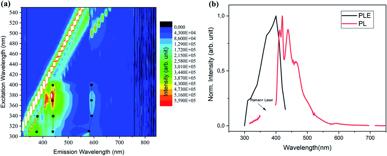 | ||
| Fig. 1 (a) Contour plots of the PL spectra at varied excitation wavelengths measured from the ball-milled sample. (b) PLE (for the 450 nm PL; black line) and PL (for the 370 nm excitation; red line), for the ball-milled sample. | ||
Interestingly, a pronounced peak structure is observed in the PL emission of the resonantly excited PL spectrum (Fig. 1b and 2a). A similar structure is also observed in the PL excited at 300 nm (Fig. 2b), but it is less pronounced. Fitting both spectra with multiple Gaussian peaks without any constraints (not shown), we found that they can be described by individual peaks with separation energies shown by the red lines in the FTIR absorption spectrum in Fig. 2c. The peak positions coincide with several Si–C and Si–O related peaks, suggesting that the PL structure might be a result of Si–C or Si–O surface vibrations coupled to the exciton. The roughly constant energies between the peak positions (red lines) are indeed reminiscent of phonon replicas (presented as a histogram) and mostly coincide with the weak vibrations of Si–C stretching at 1265 cm−1 (∼160 meV), similarly to observations in ref. 24 on alkyl-capped SiNCs. Strong absorption peaks at 1070 cm−1 can be assigned to Si–O–Si bond vibrations, confirming the presence of oxide, which is interesting and can be correlated with the experimental procedure. During the ball milling, diffusion of C from the wall and balls may have taken place to introduce Si–C bonds, but could not saturate the whole SiNC surface, allowing subsequent oxidation. Nevertheless, the Si–O bond does not seem to play an important role in the vibrational structure of the PL. This does not rule out the possible role of metallic impurities in the emission process, however, we are not aware of such vibrational states at 160 meV for Si–Fe, Co–O, Fe–C, Co–C or Si–Co bonds. The presence of O–H and C–H bond stretching in the FTIR is most likely due to the residual presence of ethanol that was used as a solvent for the measurements.
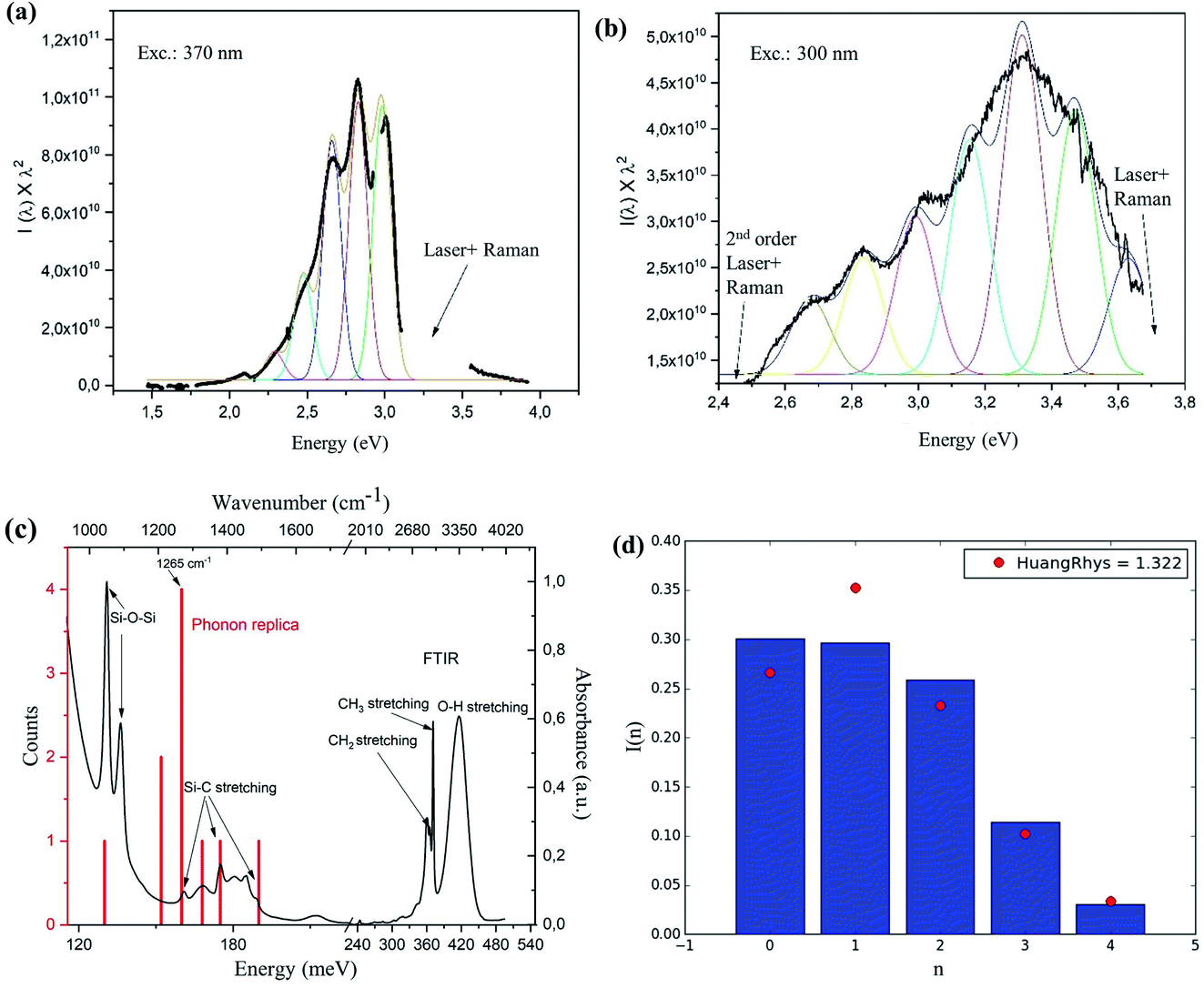 | ||
| Fig. 2 PL spectra obtained at (a) excitation of 370 nm and (b) excitation at 300 nm. PL spectra were fitted with peak difference (∼160 meV) and FWHM (140 meV) – parameters obtained first from fitting the most prominent three peaks in the spectrum shown in (a). The rest of the PL spectra were fitted with the fixed peak separation and FWHM and varying only the peak intensities. The colored peaks are the fits and the bold black curve is the original data. For better clarity, Raman and second order excitation peaks were removed from the data sets (labeled gaps in the data in the graphs in (a) and (b)). (c) FTIR spectrum showing infrared absorption (black) of the ball milled SiNCs dispersed in ethanol and the position of the peak separation energies obtained from the freely-fitted (i.e. without any fixed or assumed parameters) PL spectra excited at 300 and 370 nm. (d) Fitted intensities of the peaks in (a) and Huang-Rhys factor fit curve (red dots). | ||
Assuming that the structure in the PL spectra is related to phonon replicas, we imposed fixed peak distances of 160 meV and a FWHM of 140 meV (parameter found from free fitting the three dominant peaks in Fig. 2a), and tried to fit the PL spectra in Fig. 2a and b, varying only the peak intensities. The resulting spectrum is shown as a thin black line in the figures and the colored lines are the fits; surprisingly, the agreement of such ‘forced’ fit with the whole measured PL spectral shape is very good, indicating that the PL spectrum consists of the main zero-phonon replica (at 3.0 eV for excitation at 370 nm and at 3.65 eV for excitation at 300 nm) and related series of phonon replicas. The large number of visible replicas is very surprising, since this indicates unusually strong exciton-phonon coupling.
It is known an that impurity atom can act as a localized emission center, possibly resulting in considerable exciton-phonon coupling, responsible for the occurrence of phonon replicas in PL emission (and related effective heating of the lattice of a material via optical excitation). The strength of the coupling can be quantified by the Huang-Rhys factor S, which can be extracted from fitting the peak intensities of the phonon replicas in the spectrum, labeled from the highest energy one (0th peak) to the lowest energy one (nth peak) using the Poisson distribution
| I(n) = e−SSn/n!, with n = 0,1,2… |
The exciton-phonon coupling is considered weak for S ≤ 1, medium for S = 5–10 and strong for S > 20. In the case of Si, generally, there is a very weak coupling with S = 0.2 to 1 where the value of S varies with the bandgap and the corresponding size of the nanocrystals.41–43 In the SiNCs, enhanced coupling could appear due to the lowered symmetry and the increased role of the surface with flexible and vibrationally energetic ligands.24 By fitting the structure in Fig. 2a, we found S = 1.32 (Fig. 2d), which is very high for a Si-based material.
Since, to the best of our knowledge, such high exciton-phonon coupling has not been reported from alkyl-capped SiNCs (Si–C) or oxidized SiNCs (Si–O), it is unlikely that the Si–O or Si–C vibrations caused such a highly structured PL, which lends credence to the possibility of the involvement of transition metal impurities in the emission process. McVey et al. reported a similar PL emission structure in their study of the optical properties of SiNCs doped with transition metals (Mn, Ni and Cu).44 However, they focused more on the shift in PL peak position because of the doping of transition elements and concluded that the Si–Si bonds were the source of PL emission. In our case, the source of emission and periodic feature remains uncertain, however, the working hypothesis is that the emission is of extrinsic origin, possibly related to metallic impurities, with strong exciton-phonon coupling to the Si–C surface bonds.
To further analyze the possible size-dependence of the PL, we measured the PL from single SiNCs using an optical microspectroscopy setup, coupled to AFM, which allowed us to correlate size and PL from a single nano-object. First, we recorded a PL image in the wide-field imaging mode (Fig. 3, left top). This was then correlated with an AFM image of the same area (Fig. 3, right top). From the comparison, we selected 5 Si nanoparticles with sizes between 5 and 20 nm. For these selected Si nanoparticles (indicated by the white squares), the emission spectra were recorded by using a slit to reduce the detected area. To minimize differences due to other parameters, such as integration time and laser power gain, the spectra of all the particles were recorded with the same integration time (5 seconds) and excitation power (gain of 80%). Interestingly, we found no change in the PL peak position for the different particles. Furthermore, the PL spectral shape (width and multi-phonon peak structure) appears to be the same for the ensemble and separate nanoparticle measurements.
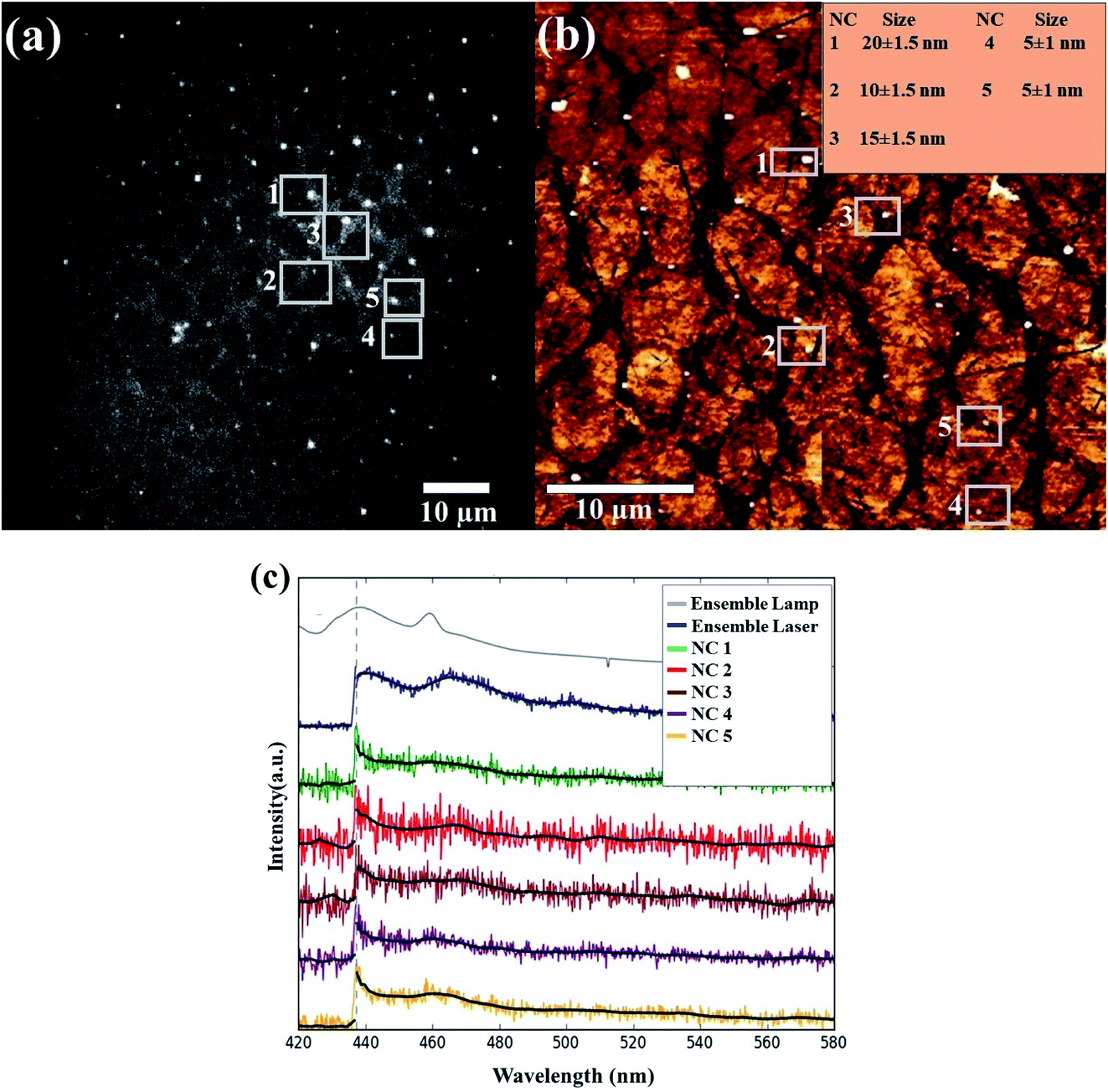 | ||
| Fig. 3 (a) PL image correlated with (b) AFM scan of the ball milled sample. The 5 selected emitting dots in the PL image and AFM are presented in the white square boxes. (c) PL spectrum of the NC ensemble excited at 405 nm using a Xe lamp (in Fluorolog setup) (gray) and the NC ensemble excited at 405 nm in the microscope setup (blue), together with 5 different single NCs selected in the AFM/PL image scans. A dotted line indicates the edge of the long-pass filter at 438 nm, used in the measurement to cut out the excitation light. The black line in every spectrum is the average of the data points to reduce noise and show a clear visual of the spectrum. | ||
Analyzing the drop-casted milled SiNC sample on a quartz slide by AFM, we also found some intriguing superstructures (Fig. 4a), probably resulting from the ‘coffee-stain’ type drying process. The larger sized objects (∼35–70 nm) showed high intensity emission in comparison to the smaller sized ones (∼5–20 nm), possibly due to a larger number of included SiNCs.
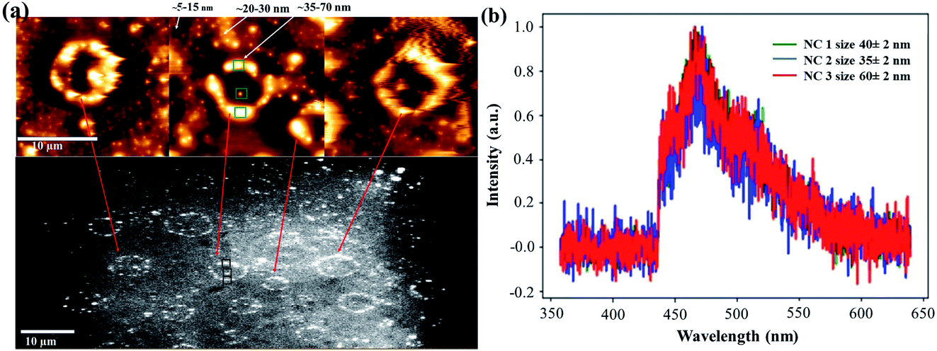 | ||
| Fig. 4 (a) Formation of Si superstructures observed by AFM-spectroscopy (top) correlated with the PL imaging (bottom) in the drop-casted milled Si powder particles on a quartz substrate. (b) Normalized PL spectra recorded in three different places (shown in green (AFM) and black (PL) square boxes) with objects of sizes in the range of 35–70 nm. | ||
Fig. 4b shows PL spectra of the larger sized object (∼35–70 nm), which appears again to be very similar to the ensemble PL spectrum (Fig. 2 and 3).
All of our optical results indicate that ball-milled SiNC powders have size-independent, blue-green emission with strong phonon replica features. The observed PL has a fast mono-exponential decay of lifetime ∼6.5 ns, as measured from the ensemble of milled SiNCs using our microscope setup (at 405 nm laser excitation, integration time ∼1800 s) (Fig. S6†). Blue PL with fast decay has been previously observed from oxygen-related defect states.45 Since the sizes of the SiNCs were found from HRTEM and AFM to be very large (>5 nm), indicating bulk-Si-like band-gaps, the emission is probably not of an intrinsic origin. Similar strong size-independent blue-green emission has been observed in the past from very small oxidized SiNCs,3,45,47 which however in larger SiNCs, such as ours, usually switches to a size-independent red emission band46,47 or a size-dependent NIR peak in even larger SiNCs.48 Therefore, it is unlikely that the observed emission originates from the Si–O centers. The energy of the phonon replica is observed here to be of 160 meV, which coincides with Si–C bonds. Liu et al.49 reported similar PL spectra from SiC NCs embedded in a SiO2 matrix with the conclusion that it could originate from either the Si–C sites or oxide defects. Another interesting work was reported by Askari et al.50 who observed a similar PL structure from SiC NCs prepared by atmospheric pressure plasmas. They indicated an unclear origin of the multiple non-shifting spectral peaks, but ruled out defect-related emission.50 McVay et al.44 used UV-assisted hydrosilylation to create a strong covalent Si–C bonded passivation (hexane capped SiNCs) to protect Si from oxidation, which also suggests the possibility of such emission by Si–C related sites. They observed multiple peak emission from both doped (metals: Cu, Mn) and undoped Si which led to the belief that Si–C sites could be the possible cause of the observed emission. However, unlike us, they observed a shift in the PL spectra with change in excitation wavelength, but it was observed to be more pronounced in the undoped Si. Interestingly, they observed spectral shape and FWHM changes under the different excitation wavelengths, pointing towards the involvement of multiple active emission centers, in which metallic impurities might have played a role as well. In our case, we suggest that the most possible model that could explain the observed bright blue-green emission is emission from an extrinsic site that is excited via energy transfer from the Si core. The extrinsic site is either Si–C related (such as the 2.86–3.02 eV emission observed in 6H–SiC50) or related to metallic impurities (Co and Fe) with Ec,Co at 2.81 eV, Ec,Fe at 2.91 eV, Ev,Co at 0.46 eV and Ev,Fe at 0.09 eV in silicon.51 Solubility of the transition metals in Si is very low because of the low diffusion coefficient, so these impurities must have been present directly on or near to the surface of the SiNCs. In such a case, it could also be possible that the emission originates from the metal impurity, which is strongly coupled to the Si–C bond vibrational states that show up in the PL spectra as phonon replicas. Nevertheless, the solubility increases at the high temperatures generated during the ball milling process. Also, the process induces several dislocations which could serve as vacancies for foreign elements, thereby causing substitutional insertion in the Si volume.
Conclusions
High-energy ball milling can be a simple, low cost and environmentally friendly way to synthesize highly emissive SiNCs. We found SiNCs as small as 5 nm in the milled sample, which makes this method very promising. The PL emission of all observed SiNCs was, however, independent of the NC size and was observed in the blue-green spectral region with a PL lifetime of a few nanoseconds. Our results suggest that the presence of metallic impurities as well as Si–C sites on the surface could play an active role. The multi-phonon structure observed in the PL emission spectra indicates that the emissive center is strongly vibrationally coupled to Si–C bonds. The effect of strain, that – beyond the mere introduction of vacancies and defects – could serve as possible sites for Fe, C, O and Co incorporation, needs to be studied in more detail in the future e.g. by studying samples produced with different ball milling times. The interesting superstructures observed in the drop-casted sample could be used for anti-counterfeiting or labelling applications.Conflicts of interest
There are no conflicts to declare.Acknowledgements
Ankit Goyal is thankful to the financial support provided by the Institute of Physics at the University of Amsterdam.References
- M. V. Wolkin, J. Jorne, M. Fauchet, G. Allan and C. Delerue, Phys. Rev. Lett., 1999, 82, 197, DOI:10.1103/physrevlett.82.197.
- N. Shirahata, T. Hasegawa, Y. Sakka and T. Tsuruoka, Small, 2010, 6(8), 915–921 CrossRef CAS PubMed.
- K. Dohnalová, T. Gregorkiewicz and K. Kůsová, J. Phys.: Condens. Matter, 2014, 26(17), 173201 CrossRef PubMed.
- D. Tan, B. Xu, P. Chen, Y. Dai, S. Zhou, G. Ma and J. Qiu, RSC Adv., 2012, 2, 8254–8257 RSC.
- J. H. Warner, A. Hoshino, K. Yamamoto and R. D. Tilley, Angew. Chem., 2015, 117, 4626–4630 CrossRef.
- J. P. Wilcoxon, G. A. Samara and P. N. Provencio, Phys. Rev. B: Condens. Matter Mater. Phys., 1999, 60(4), 2704 CrossRef CAS.
- D. S. English, L. S. Pell, Z. Yu, P. F. Barbara and B. A. Korgel, Nano Lett., 2002, 27, 681–685 CrossRef.
- J. B. Miller, A. R. Sickle, R. J. Anthony, D. M. Kroll, U. R. Kortshagen and E. K. Hobbie, ACS Nano, 2012, 68, 7389–7396 CrossRef PubMed.
- X. Wen, P. Zhang, T. A. Smith, R. J. Anthony, U. R. Kortshagen, P. Yu, Y. Feng, S. Shrestha, G. Coniber and S. Huang, Sci. Rep., 2015, 5, 12469 CrossRef PubMed.
- Q. Li, Y. He, J. Chang, L. Wang, H. Chen, Y. W. Tan, H. Wang and Z. Shao, J. Am. Chem. Soc., 2013, 135(40), 14924–14927 CrossRef CAS PubMed.
- X. D. Pi, R. W. Liptak, J. D. Nowak, N. P. Wells, C. B. Carter, S. A. Campbell and U. Kortshagen, Nanotechnology, 2008, 19(24), 245603, DOI:10.1088/0957-4484/19/24/245603.
- D. Jurbergs, E. Rogojina, L. Mangolini and U. Kortshagen, Appl. Phys. Lett., 2006, 88, 233116, DOI:10.1063/1.2210788.
- L. Mangolini, D. Jurbergs, E. Rogojina and U. Kortshagen, J. Lumin., 2006, 121(2), 327–334 CrossRef CAS.
- W. Biesta, B. Lagen, V. S. Gevaert, A. T. M. Marcelis, J. M. J. Paulusse, M. W. F. Nielen and H. Zuilhof, Chem. Mater., 2012, 24, 4311–4318 CrossRef CAS.
- J. G. C. Veinot, Chem. Commun., 2006, 4160–4168, 10.1039/b607476f.
- J. P. Wilcoxon and G. A. Samara, Appl. Phys. Lett., 1999, 74(21), 3164, DOI:10.1063/1.124096.
- C. S. Yang, S. M. Kauzlarich, Y. C. Wang and H. W. H. Lee, J. Cluster Sci., 2000, 11(3), 423–431 CrossRef CAS.
- M. A. Islam, R. Sinelnikov, M. A. Howlader, A. Faramus and J. G. C. Veinot, Chem. Mater., 2018, 30(24), 8925–8931 CrossRef CAS.
- J. H. Warner, H. R. Dunlop and R. D. Tilley, J. Phys. Chem. B, 2005, 109(41), 19064–19067 CrossRef CAS.
- P. Mohapatra, D. M. Perez, J. M. Bobbitt, S. Shaw, B. Yuan, X. Tian, E. A. Smith and L. Cademartiri, ACS Appl. Mater. Interfaces, 2018, 10(24), 20740–20747 CrossRef CAS PubMed.
- Y. Zhong, X. Sun, S. Wang, F. Peng, F. Bao, Y. Su, Y. Li, S. T. Lee and Y. He, ACS Nano, 2015, 9(6), 5958–5967 CrossRef CAS PubMed.
- J. Valenta, M. Greben, S. A. Dyakov, N. A. Gippius, D. Hiller, S. Gutsch and M. Zacharias, Sci. Rep., 2019, 9, 11214 CrossRef CAS PubMed.
- K. Dohnalová, A. N. Poddubny, A. A. Prokofiev, W. D. A. M. de Boer, C. P. Umesh, J. M. J. Paulusse, H. Zuilhof and T. Gregorkiewicz, Light: Sci. Appl., 2013, 2, e47 CrossRef.
- K. Dohnalová, A. Fučiková, C. P. Umesh, J. Humpoličková, J. M. J. Paulusse, J. Valenta, H. Zuilhof, M. Hof and T. Gregorkiewicz, Small, 2012, 8(20), 3185–3191 CrossRef PubMed.
- S. P. Pujari, H. Driss, F. Bannani, B. Lagen and H. Zuilhof, Chem. Mater., 2018, 30(18), 6503–6512 CrossRef CAS PubMed.
- M. Dasog, Z. Yang, S. Regli, T. M. Atkins, A. Faramus, M. P. Singh, E. Muthuswamy, S. M. Kauzlarich, R. D. Tilley and J. G. C. Veinot, ACS Nano, 2013, 73, 2676–2685 CrossRef PubMed.
- J. Fuzell, A. Thibert, T. M. Atkins, M. Dasog, E. Busby, J. G. C. Veinot, S. M. Kauzlarich and D. S. Larsen, J. Phys. Chem. Lett., 2013, 4(21), 3806–3812 CrossRef CAS.
- Y. Kanemitsu and S. Okamoto, Phys. Rev. B: Condens. Matter Mater. Phys., 1997, 55(12), 7375, DOI:10.1103/physrevb.55.r7375.
- G. Belomoin, J. Therrien and M. Nayfeh, Appl. Phys. Lett., 2000, 77, 779, DOI:10.1063/1.1306659.
- J. Valenta, A. Fucikova, I. Pelant, K. Kusova, K. Dohnalova, A. Aleknavicius, O. Cibulka, A. Fojtik and G. Kada, New J. Phys., 2008, 10, 073022 CrossRef.
- Z. Kang, Y. Liu, C. H. A. Tsang, D. D. D. Ma, X. Fan, N. B. Wong and S. T. Lee, Adv. Mater., 2009, 21, 661–664 CrossRef CAS.
- F. Hua, M. T. Swihart and E. Ruckenstein, Langmuir, 2005, 21(13), 6054–6062 CrossRef CAS PubMed.
- D. Beri, D. Busko, A. Mazilkin, I. A. Howard, B. S. Richards and A. Turshatov, RSC Adv., 2018, 8, 9979–9984 RSC.
- D. M. Lyons, K. M. Ryan, M. A. Morris and J. D. Holmes, Nano Lett., 2002, 28, 811–816 CrossRef.
- K. Kusova, Phys. Status Solidi A, 2018, 215, 1700718 CrossRef.
- K. Kůsová, P. Hapala, J. Valenta, P. Jelínek, O. Cibulka, L. Ondič and I. Pelant, Adv. Mater. Interfaces, 2014, 1, 1300042 CrossRef.
- G. Lv, B. Zhu, X. Li, C. Chen, J. Li, Y. Jin, X. Hu and J. Zhu, ACS Appl. Mater. Interfaces, 2017, 951, 44452–44457 CrossRef PubMed.
- C. Suryanarayana, Prog. Mater. Sci., 2001, 46, 1–184 CrossRef CAS.
- E. R. Weber, Appl. Phys. A: Solids Surf., 1983, 30, 1–22 CrossRef.
- I. D. Wolf, Semicond. Sci. Technol., 1996, 11, 139–154 CrossRef.
- T. Takagahara, J. Lumin., 1996, 70, 129–143 CrossRef CAS.
- J. Martin, F. Cichos, F. Huisken and C. Borczyskowski, Nano Lett., 2008, 8(2), 656–660 CrossRef CAS PubMed.
- I. Pelant, J. Hala, M. Ambroz, M. Vacha, J. Valenta, F. Adamec, V. Kohlova and J. Matouskova, Impurity assessment in Si wafers by photoluminescence method V. Research report for Tesla Roznov, Charles University in Prague, Faculty of Mathematics and Physics, Prague, 1990 Search PubMed.
- B. F. P. McVey, J. Butkus, J. E. Halpert, J. M. Hodgkiss and R. D. Tilley, J. Phys. Chem. Lett., 2015, 6, 1573–1576 CrossRef CAS PubMed.
- L. Tsybeskov, J. V. Vandyshev and P. M. Fauchet, Phys. Rev. B: Condens. Matter Mater. Phys., 1994, 49(11), 7821–7824 CrossRef CAS PubMed.
- K. Dohnalová, K. Kůsová and I. Pelant, Appl. Phys. Lett., 2009, 94, 211903, DOI:10.1063/1.3141481.
- K. Dohnalová, L. Ondič, K. Kůsová, I. Pelant, J. L. Rehspringer and R. R. Mafouana, J. Appl. Phys., 2010, 107, 053102, DOI:10.1063/1.3289719.
- Y. Kanzawa, T. Kageyama, S. Takeoka, M. Fujii, S. Hayashi and K. Yamamoto, Solid State Commun., 1997, 102(7), 533–537 CrossRef CAS.
- X. Liu, J. Zhang, Z. Yan, S. Ma and Y. Wang, Mater. Phys. Mech., 2001, 4, 85–88 CAS.
- S. Askari, A. U. Haq, M. M. Montero, I. Levchenko, F. Yu, W. Zhou, K. Ostrikov, P. Maguire, V. Svrcek and D. Mariotti, Nanoscale, 2016, 8, 17141–17149 RSC.
- E. B. Yakimov, Metal Impurities and Gettering in Crystalline Silicon, in Handbook of Photovoltaic Silicon, ed. D. Yang, Springer, Berlin, Heidelberg, 2019 Search PubMed.
Footnote |
| † Electronic supplementary information (ESI) available. See DOI: 10.1039/c9fd00105k |
| This journal is © The Royal Society of Chemistry 2020 |