
 Open Access Article
 This Open Access Article is licensed under a
 Creative Commons Attribution 3.0 Unported Licence
Expression of interfacial Seebeck coefficient through grain boundary engineering with multi-layer graphene nanoplatelets†
Yue
Lin‡
 ab,
Maxwell
Wood‡
a,
Kazuki
Imasato‡
a,
Jimmy Jiahong
Kuo‡
a,
David
Lam
a,
Anna N.
Mortazavi
cd,
Tyler J.
Slade
e,
Stephen A.
Hodge
f,
Kai
Xi
g,
Mercouri G.
Kanatzidis
e,
David R.
Clarke
c,
Mark C.
Hersam
ae and
G. Jeffrey
Snyder
*a
ab,
Maxwell
Wood‡
a,
Kazuki
Imasato‡
a,
Jimmy Jiahong
Kuo‡
a,
David
Lam
a,
Anna N.
Mortazavi
cd,
Tyler J.
Slade
e,
Stephen A.
Hodge
f,
Kai
Xi
g,
Mercouri G.
Kanatzidis
e,
David R.
Clarke
c,
Mark C.
Hersam
ae and
G. Jeffrey
Snyder
*a
aDepartment of Materials Science and Engineering, Northwestern University, IL 60208, USA. E-mail: alexyue.lin@gmail.com; jeff.snyder@northwestern.edu
bCavendish Laboratory, University of Cambridge, Cambridge CB3 0HE, UK
cSchool of Engineering and Applied Sciences, Harvard University, Cambridge, MA 02138, USA
dDepartment of Materials Science and Engineering, Monash University, Clayton, VIC 3800, Australia
eDepartment of Chemistry, Northwestern University, IL 60208, USA
fVersarien Plc, Cheltenham GL51 9LT, UK
gDepartment of Materials Science and Metallurgy, University of Cambridge, Cambridge CB3 0FS, UK
First published on 24th September 2020
Abstract
Energy filtering has been a long-sought strategy to enhance a thermoelectric material's figure of merit zT through improving its power factor. Here we show a composite of multi-layer graphene nanoplatelets (GNP) and n-type Mg3Sb2 leads to the expression of an energy filtering like effect demonstrated by an increase in the material's Seebeck coefficient and maximum power factor, without impact on the material's carrier concentration. We analyse these findings from the perspective of a heterogeneous material consisting of grain and grain boundary phases, instead of a more traditional and common analysis that assumes a homogeneously transporting medium. An important implication of this treatment is that it leads to the development of an interfacial Seebeck coefficient term, which can explain the observed increase in the material's Seebeck coefficient. The contribution of this interfacial Seebeck coefficient to the overall Seebeck coefficient is determined by the relative temperature drop across the grain boundary region compared to that of the bulk material. In Te doped Mg3Sb2 we show the introduction of GNP increases the interfacial thermal resistance of grain boundaries, enhancing the contribution of the interfacial Seebeck coefficient arising from grain boundaries to the overall Seebeck coefficient. Without significant detriment to the electrical conductivity this effect results in a net increase in maximum power factor. This increased interfacial thermal resistance also leads to the synergistic reduction of the total thermal conductivity. As a result, we enhance zT of the Mg3Sb2 to a peak value of 1.7 near 750 K. Considering the two-dimensional nature of the grain boundary interface, this grain boundary engineering strategy could be applied to a few thermoelectric systems utilizing various two-dimensional nanomaterials.
Broader contextOptimizing the thermoelectric properties in a material has always been a balancing act of inversely corelated material's properties. This counterpoise has traditionally been mediated by tuning the carrier concentration in a semiconductor as to strike an optimal balance between the material's Seebeck coefficient and conductivity. Energy filtering is a concept that thinks outside the box of this common paradigm and offers a mechanism to boost a material's Seebeck coefficient without a change in the semiconductor's carrier concentration. While a long-sought strategy to enhance thermoelectric performance, energy filtering has had few successful demonstrations to date. We revisit the concept from a heterogeneous perspective and reveal a missing key to be an interfacial Seebeck coefficient. Using Mg3Sb2 as an example material, we experimentally demonstrate a grain boundary engineering approach to realize the benefit of energy filtering, through the addition of graphene. We observe an over 40% increase in the material's high temperature zT (1.73 near 773 K), without changing the material's carrier concentration. This work provides a framework to understand energy filtering using the interfacial Seebeck coefficient. We anticipate the interfacial Seebeck concept together with the experimental strategy utilizing graphene will catalyse the growth of interface and grain boundary engineering of thermoelectric materials. |
1 Introduction
Electron filtering1,2 was theoretically proposed3,4 to enhance the thermoelectric power factor (PF = α2σ) of materials. In an n-type semiconductor, low energy electrons have a smaller contribution to the material's Seebeck coefficient (α).5,6 An energy filtering approach surmises that these low energy electrons can be preferentially blocked by an energy barrier, resulting in an increase in thermopower (the magnitude of Seebeck coefficient). One way that has been postulated to introduce the energy barriers is through creation of grain boundaries (Fig. 1a).5,7 The existence of grain boundaries may also scatter phonons, resulting in a reduction in lattice thermal conductivity (κL).8 In this case, the figure of merit9zT (zT = PF/κ) would be enhanced through the synergistic effect of a rise in power factor (often used as a signature of energy filtering) and a reduction in thermal conductivity (κ = κe + κL, where κe is electronic contribution of the thermal conductivity). However, the existence of boundaries can substantially reduce a material's mobility and therefore its electrical conductivity (σ).10 In order for these barriers to increase α2σ, any reduction in σ must be compensated by an increase in α2 such that the overall α2σ is increased. In practice there are few successful demonstrations of an improvement of α2σ and no viable thermoelectric materials with improved zT via an energy filtering strategy.7,11,12 A possible reason why previous studies have struggled is due to a disconnect between theoretical and experimental approaches. While most experimental studies of energy filtering acknowledge inhomogeneity in their material is important to create an energy filtering effect,13,14 most if not all theoretical analysis is done using a homogenous transport theory1,15,16 (see S1 in ESI,† for brief review of previous experimental work dealing with the energy filtering concept). In most cases, electron barriers at grain boundaries do more harm than good to the electronic properties of thermoelectric materials. In the recently discovered n-type thermoelectric material Mg3Sb217,18 this has become extremely apparent. Mg3Sb2 is an example of a material with charged grain boundaries that lead to an energy offset (ΔE) between the conduction band minimum (CBM) in the grain and that of the grain boundary (Fig. 1a).10 This physical picture is essentially the same as what is predicted to increase a material's Seebeck coefficient through electron filtering.11,12 However, instead of benefitting from grain boundaries, previous reports on n-type Mg3Sb1.5Bi0.5 have found significantly lower thermoelectric performance with smaller grains. This has been traced to the added electrical resistance at grain boundaries where the effect of grain boundaries10 on the lattice thermal conductivity and Seebeck coefficient was reported as largely negligible.19,20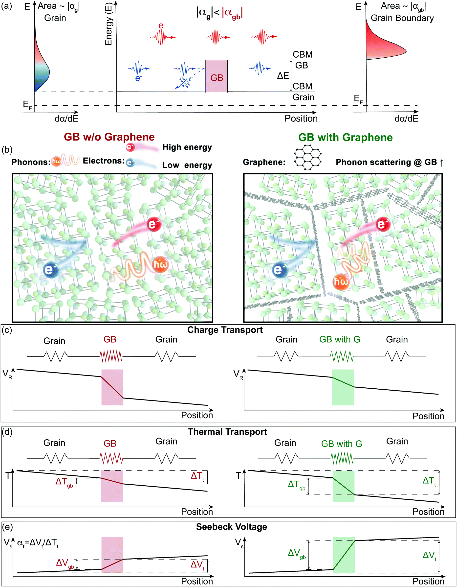 | ||
| Fig. 1 Illustration of the energy filtering effect in polycrystalline Mg3Sb2 with electron filtering at the grain boundaries (GB). (a) The high energy electrons contribute more to the Seebeck coefficient than the low energy electrons. By changing the band structure at the grain boundaries, the low energy electrons can be preferentially “filtered out”, therefore increasing the magnitude of the Seebeck coefficient. The band offset (ΔE) between the conduction band minimum (CBM) of the grain and the grain boundary (GB) acts as the electron filter so that the grain boundary region has a larger magnitude of the Seebeck coefficient (|αgb| > |αg|). (b) to (e) Electron and Phonon transport in the samples without (left) and with (right) GNP (G) at the grain boundaries modelled as a series circuit. Grain boundaries in our model are more electrically and thermally restive than the bulk material, which leads to an additional resistance voltage (VR) drop and temperature (T) drop. We find the addition of GNP does not introduce an additional barrier for electron transport but does increase the interfacial thermal resistance at the boundaries. Based on our two-phase model, an increased thermal resistance at grain boundaries will lead to an increased temperature drop in the grain boundary phase (ΔTgb) of the material (d), thus a larger grain boundary voltage (ΔVgb = αgbΔTgb) (e). Due to the grain boundary Seebeck coefficient being larger than the bulk Seebeck coefficient (|αgb| > |αg|), the enhanced temperature drop in the grain boundary phase increases the magnitude of the overall Seebeck coefficient (|αt|, see eqn (1)). | ||
This reality suggests that any grain boundary engineering strategies that include energy filtering to improve zT must carefully weigh the effects on all transport properties. Interfaces such as grain boundaries are frequently introduced into thermoelectric materials to reduce the phonon mediated or lattice thermal conductivity. Typically, the hope is that such interfaces effectively lower lattice thermal conductivity without significantly hindering the electron mobility. Strategies to improve the effectiveness of grain boundaries, by increasing the thermal interface resistance of each boundary have been successful in a few examples.21–23 Inserting nano-carbon additives (i.e. graphene24 and carbon nanotube) to grain boundaries of these materials has successfully reduced lattice thermal conductivity without significant detriment to the conductivity. Thus, carefully engineered grain boundaries with combined electronic and thermal effects could lead to improved zT.
Interfacial thermal resistance is typically described as a Kapitza resistance25,26 where the resistance occurs across a two-dimensional interface. Although the interfacial region could be several-nanometres in thickness,27 the thermal properties can be sufficiently described without defining a thickness. Considering polycrystalline materials as a heterogeneous material consisting of grain regions and interfacial grain boundary regions enables quantitative understanding of the interfacial effects of both thermal and electrical resistances as additional resistors in series with the grain resistance.
In this work, we demonstrate how using a self-consistent two-phase model for electronic (Fig. 1c) and thermal transport (Fig. 1d) can lead to effects that could be interpreted as energy filtering. The energy offset at grain boundaries in materials with charged grain boundaries like Mg3Sb2 leads the interfacial region to be more electrically resistive but also have a larger Seebeck coefficient compared to the bulk. We find that the key to observe an energy filtering effect is to maximize the temperature drop across the grain boundary region. We use this insight to explain energy filtering effects witnessed in magnesium antimonide (Mg3.2Sb1.99Te0.01) composited with GNP.28 The addition of GNP increases interfacial thermal resistance at the grain boundaries (Fig. 1b) and thus increases the temperature drop across the grain boundary region (Fig. 1d). This in turn leads to an increased expression of the interfacial Seebeck coefficient arising from grain boundaries that adds to the total Seebeck coefficient, which enhances the material's maximum power factor and figure of merit zT (Fig. 2).
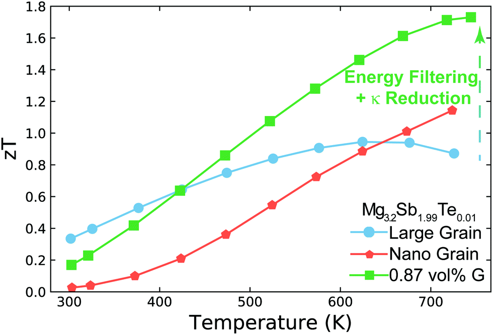 | ||
| Fig. 2 Temperature dependent zT of Mg3.2Sb1.99Te0.01 (nominal composition29) and its nanocomposite with GNP (G). Large grain Mg3.2Sb1.99Te0.01 has a peak zT of ∼0.95 near 650 K, which is increased to ∼1.7 near 750 K with the addition of GNP. This enhancement is a result of increasing the interfacial thermal resistance at grain boundaries with the addition of GNP. This increased thermal resistance leads to the synergistic outcomes of reducing the sample's thermal conductivity as well as amplifying its Seebeck coefficient via an energy filtering effect. In nano-grained Mg3.2Sb1.99Te0.01, the performance is limited due to significant grain boundary electrical resistance. While the nano-grained sample's Seebeck coefficient is increased by the energy filtering effect, the enhancement is not large enough to compensate the reduction in electrical conductivity's impact on power factor. The zT enhancement for the nano-grained sample above 650 K in this case is primarily due to the sample's reduction in thermal conductivity. Note that the electrical conductivity and Seebeck coefficient used here are all measured in a ZEM-3 for the purpose of comparison to state-of-the-art of n-type Mg3Sb2 based compounds in literature (see S2, ESI†). | ||
2 A two-phase description for a heterogeneous material with grain boundaries
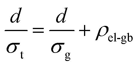
In a material with grain boundaries, both the charge and phonon transport behaviour are different in grains and at grain boundaries. A charge barrier at a grain boundary has the effect of adding an interfacial resistance at the grain boundaries (Fig. 1c).30–32 Meanwhile the potential barrier, or band offset at the grain boundary (Fig. 1a) should lead to the grain boundary region having a larger magnitude of the Seebeck coefficient |α| compared to the rest of the bulk.33 On the other hand, phonon transport is influenced by the structural difference at the grain boundaries such as lattice mismatch, which induces additional interfacial thermal resistance (Kapitza resistance) at the grain boundaries.25,34 As a result, a material with charged grain boundaries can be better understood under a two-phase model consisting of grain phase and grain boundary phase. In this model, the grain phases and grain boundary phases are connected in a series circuit (Fig. 1c and d), which is one of the limiting cases of effective medium theory.35–37 We use this simplified model to simulate and explain the Seebeck coefficient, thermal conductivity, and electrical conductivity of the material made up of grain and grain boundary phases. We acknowledge that in reality the transport occurs over a three-dimensional network of grains/grain boundaries, where both series and parallel conduction could co-exist. However, the parallel conduction through grain boundaries has marginal effect on the overall transport properties, as in parallel case the contribution of each phase is weighted by electrical conductivity.38 Thus, our series model provides a reasonable approximation for the real case.For a heterogeneous material of grain and grain boundary phase with a total temperature drop ΔTt, the apparent overall Seebeck coefficient αt will be (see S3.1 in ESI,† for detailed derivation):
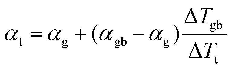 | (1) |
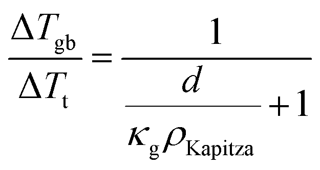 | (2) |
Here, κg is thermal conductivity of the grain phase.
3 Results and discussion
3.1 Physical characterisation
Based on SEM (Fig. S8, ESI†) and TEM (Fig. S10, ESI†) analysis, we confirm that GNP is generally well distributed in the Mg3.2Sb1.99Te0.01 matrix without much localised aggregation (further shown by Raman spectroscopy (Fig. S12, ESI†)). The material at the grain boundaries is identified as GNP24 with average thickness of ∼3 nm (Fig. S10 and Section S5.10, ESI†). STEM-EDX (Fig. S11, ESI†) analysis shows the presence of MgO between grains. The existence of charged grain boundaries in Mg3Sb2 have been previously rationalized by the presence of Mg vacancies in the grain boundaries,10 where MgO could be involved in the removal of Mg as de Boor41et al. has shown in Mg2Si. (See session S5.4 for detailed discussion, ESI†). Both XRD (Fig. S13, ESI†) and XPS (Fig. S14, ESI†) analysis confirms that the introduction of GNP does not introduce detectable structural and compositional change at a bulk scale.3.2 Transport implications of energy filtering in Mg3Sb2Mg3Sb2
An effect analogous to electron filtering is observed in Te doped Mg3Sb2 by increasing the ratio of the temperature drop across grain boundaries to the total temperature drop across the sample ΔTgb/ΔTt. We experimentally achieve this result in two different ways. The first was realized by decreasing the grain size (nano structuring) of our material via sintering at lower temperature (see S6.3, ESI†), resulting in a larger fractional amount of grain boundary “phase” in our sample. The second was realized by compositing of our material with GNP, which increased the interfacial thermal resistance at the grain boundaries. As a control we compare our samples with the energy filtering effect to a large grain sample in which the grain boundary contribution to electron and thermal transport is minimized.By increasing ΔTgb/ΔTtvia these methods we see the Seebeck coefficient of the Mg3.2Sb1.99Te0.01 is enhanced to varying degrees compared to that of large grain sample (Fig. 3d). In a typical thermoelectric material, an increase in a sample's Seebeck coefficient is coupled with a decrease in the material's carrier concentration. However, from Hall measurements (insert of Fig. 3b and Fig. S4d, ESI†) we do not observe a decrease in carrier concentration suggesting the increased Seebeck coefficient comes from an energy filtering-like effect. Furthermore, the electrical conductivity (Fig. 3c) of all samples begins to converge to a similar value at higher temperatures, where grain boundary scattering of electrons is less strong.10 Therefore, we ascribe the observed changes of transport properties to microstructural changes rather than difference in carrier concentration of the bulk material. Note, the hall coefficient of poly-crystalline semiconductors is unaffected by the presence of grain boundaries in the limits where grain boundaries are highly resistive or much thinner than the grain.42,43
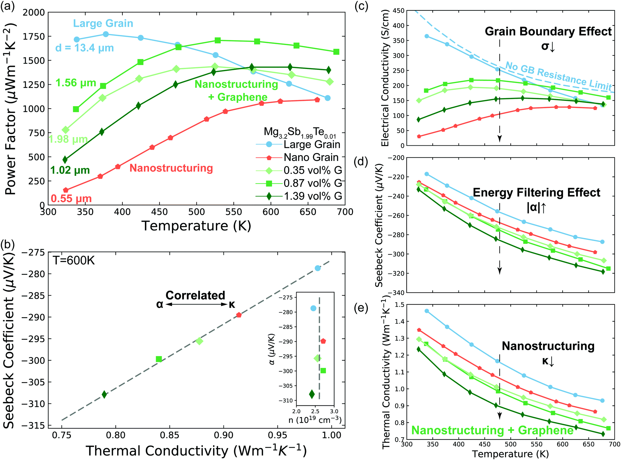 | ||
| Fig. 3 Transport properties of Mg3.2Sb1.99Te0.01 with varying grain size and GNP concentration (G) concentration. (a) Temperature dependent power factor of the samples. The average grain size d of each sample was measured by EBSD (S5.2, ESI†). (b) Linear correlation between Seebeck coefficient and thermal conductivity. The samples with lower thermal conductivity show larger Seebeck coefficient, signalling the importance of grain boundary Kapitza resistance on the energy filtering effect. The data points are extracted from the smooth fitted curves in d. The Dashed line is a guide to the eye, which can also be applied to give the value of the interfacial Seebeck coefficient (the intercept at κt = 0) by applying eqn (3). See Fig. S6 (ESI†) for other temperatures. The insert is measured Hall carrier concentration versus measured Seebeck coefficient of Mg3.2Sb1.99Te0.01 samples at 600 K. The samples have the same carrier concentration (2.6 ± 0.2 × 1019 cm−3, indicated as the dashed line) without dependency on the Seebeck coefficient. (c) to (e) Seebeck coefficient, electrical conductivity and thermal conductivity of the samples. The no grain boundary (GB) resistance limit (c) is estimated by assuming acoustic-phonon scattering (T−3/2) is the sole scattering mechanism.10 Note here the enhancement in Seebeck coefficient (d) is not as a result of a reduction in carrier concentration as measured by Hall effect (see Fig. 3b and Fig. S4d, ESI†). In the high temperature range where the influence of grain boundaries is significantly reduced, the electrical conductivity of all samples begins to converge, further supporting the assertion that the samples all have the same carrier concentration. Please see session S4 in ESI,† for repeatability of the measurements. | ||
Further evidence that an energy filtering effect is present is this system is given by the correlated behaviour of the sample's overall Seebeck coefficient (αt) and thermal conductivity (κt) shown in Fig. 3b according eqn (3).
 | (3) |
All of the samples are well described by a single slope (Fig. 3b and Fig. S6, ESI†) as predicted from eqn (3) if αg, αgb and κg remain constant under the same temperature, suggesting the presence of an energy filtering effect. While the concept of interfacial thermal or electrical resistances are common the idea of an interfacial Seebeck coefficient αgb is not. The Seebeck coefficient is an electronic transport property like conductivity and so it should not be surprising that an interfacial Seebeck coefficient resulting from the energy filtering should exist along with interfacial resistance.
3.3 Grain boundary engineering with GNP to amplify energy filtering effect in Mg3.2Sb2
Based on the temperature dependence of conductivity (Fig. 3c), the large grain Mg3.2Sb2 sample shows little grain boundary effect. Therefore we can assume the large grained sample's other transport properties are close to those expected of a single crystal with no grain boundaries.10 By assuming the Seebeck coefficient and thermal conductivity of the large grain sample from Fig. 3d and e represents αg and κg, we extract the αg (shown as hollow points in Fig. 4a) and κg from smooth fitted curve of the large grain sample between 300 K to 650 K with a step of 50 K. For calculation of αgb, we also extract αt and κt from smooth fitted curves of the other samples in Fig. 3d and e. By applying this procedure we can estimate the αgb in the Mg3.2Sb1.99Te0.01 samples with and without our addition of GNP and found the grain boundary Seebeck coefficient to be the same within experimental error in every sample (Fig. 4a). This observation suggests that the addition of GNP does not influence the energy offset of the electron filtering barrier, but may primarily acts to increase phonon scattering at the grain boundary. Structural characterization (see S5.3–S5.7, ESI†) further proved that the presence of GNP did not introduce any detectable elemental or compositional change.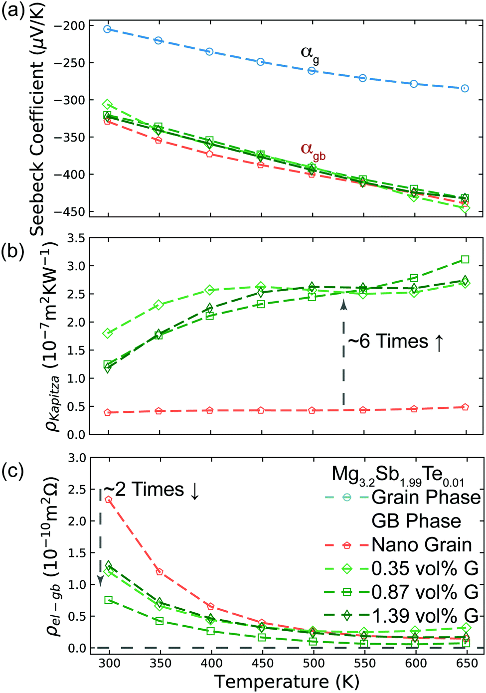 | ||
| Fig. 4 Analysis of Mg3.2Sb1.99Te0.01 samples with and without GNP using the two-phase model. (a) Seebeck coefficient of the grain phase (αg) and grain boundary phase (αgb) in the various Mg3.2Sb1.99Te0.01 samples with and without the presence of GNP. |αgb| is significantly higher than that of the grain phase, due to the presence of an energy barrier at grain boundaries. The inferred αgb of all samples are the same, reflecting the same band offset at the grain boundaries with and without GNP. αgb was inferred by applying eqn (3), while αg was extracted from the smooth fitting curve of the large grain sample in Fig. 3d between 300 K to 650 K with a step of 50 K. (b) Interfacial thermal resistance (ρKapitza) of the grain boundary phase in various Mg3.2Sb1.99Te0.01 samples. The inclusion of GNP in the grain boundary results in an increase of ρKapitza. ρKapitza was inferred by applying eqn (4) and the measured grain size (see S5.2, ESI†). (c) Interfacial electrical resistance (ρel-gb) of the grain boundary phase in various Mg3.2Sb1.99Te0.01 samples. ρel-gb was inferred by applying eqn (5). The incorporation of GNP in the grain boundary results in a decrease of ρel-gb in the temperature range below 500 K. For the range above 500 K where the energy filtering effect showing benefit, the GNP incorporation does not promote reduction of ρel-gb. | ||
Although the nano-grained sample (without GNP) exhibited an electron filtering effect, its overall power factor is significantly lower than that of the large grain sample (Fig. 3a). This observation indicates that the increase in Seebeck coefficient (Fig. 3d) by adding the electron barriers does not compensate the decrease in electrical conductivity (Fig. 3c). In contrast, the power factor of GNP/Mg3.2Sb1.99Te0.01 samples is enhanced above 500 K when compared to the large grain sample. This is a result of greater enhancement in the overall Seebeck coefficient of the bulk material (Fig. 3d) with less impact in electrical conductivity (Fig. 3c).
The total thermal resistance is a sum of thermal resistance in the grain phase and Kapitza resistance at the grain boundary. For a material with average grain size d, we have (see S3.2 for detailed derivation, ESI.†):
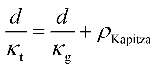 | (4) |
Here, the average grain size d can be determined by electron backscatter diffraction (EBSD, see S5.2, ESI†), enabling the estimation of ρKapitza (Fig. 4b). Compared to the nano-grained sample, the ρKapitza increased by a factor of ∼6 with the addition of GNP.
The electron transport is under the same configuration as the thermal transport:
 | (5) |
By applying the no grain boundary (GB) resistance limit (Fig. 3c) as the electrical conductivity of the grain (σg), this equation enables estimation of interfacial electrical resistivity (ρel-gb) (Fig. 4c). Compared to the nano-grained sample, the average ρel-gb remains the same with the addition of GNP in the temperature range above 500 K where the energy filtering showing benefit.
Within the experimentally derived formulations of interfacial thermal resistance ρKapitza, interfacial electrical resistance ρel-gb and interfacial Seebeck coefficient αgb, the thermoelectric efficiency across the same temperature drop can be defined in the same manner, giving an interfacial zTgb as
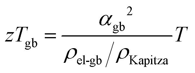 | (6) |
The improvement of the total zT (Fig. 2) is presumably a result of zTgb being greater than the bulk zT consistent with prior analysis of electron filtering.9 While the minimum thermal conductivity provides an important limit to bulk zT, Kapitza resistances are known to be able to be considerably large.44,45 In this way, the benefit of energy filtering effect was realized. Similar correlation between measured Seebeck and thermal conductivity, and significant improvement in zT were also observed in Si0.80Ge0.20B0.016 (see S5.8, ESI†).46
3.4 Experimental strategies for performance enhancement of thermoelectric materials
Our model provides a simple tool to identify and alter possible energy filtering effects in thermoelectric materials. Using a two-phase model in our system we found a key requirement for an energy filtering effect to be expressed is maximizing the temperature drop across the energy barrier region of the sample. Applying nano-carbon materials such as GNP may be an effective grain boundary engineering strategy to enhance the thermoelectric performance of a few materials. Apart from Mg3Sb2, several other thermoelectric materials47 (i.e. Ca3AlSb3, Ca5Al2Sb6, SnSe, KAlSb4, Sr3GaSb3, PbSe-NaSbSe2,48 Mg2Si41 and (Hf,Zr)CoSb Half-Heusler49) exhibit grain size dependent effects and therefore would be good candidates to explore. We suspect that a homogeneous distribution of nano-materials in a matrix is essential although challenging. For instance, due to the strong van der Waals interaction between individual graphene sheets, graphene sheet tends to aggregate easily, and forms poorly dispersed aggregations in the matrix.50 In our case, addition of 1.74 vol% GNP leads to detrimental effect to thermoelectric performance which has been traced to severely aggregation of graphene sheets in the matrix (Fig. S17, ESI†). Aggregation and/or a continuous interfacial network of nano-carbon materials should be avoided, otherwise it may lead to disturbance of electron transport and thermal shorting, which would severely impair composite performance21,23,51 (see S5.9 for further discussion, ESI†).4 Conclusion and perspective
Electron filtering has been predicted to be an effective approach in enhancing thermoelectric performance. By applying a two-phase model and introducing an interfacial Seebeck coefficient term, we shed new light onto the design principles and applications of the energy filtering concept. Examining Mg3.2Sb1.99Te0.01 as an example, we increased Kapitza thermal resistance of the grain boundary phase, by utilizing GNP as a grain boundary engineering additive. This in turn promoted temperature drop across the grain boundary region, which increased the expression of the interfacial Seebeck coefficient in Mg3.2Sb1.99Te0.01. This approach, in contrast to simply reducing grain size, minimizes the impact to electron charge transport, thus enhancing thermoelectric performance. We encourage the community to investigate the materials showing correlation of reduced thermal conductivity and rising Seebeck coefficient with nanostructuring.5 Experimental detail
5.1 Synthesis of Mg3.2Sb1.99Te0.01
The nominal composition used for all ball milled samples in this study was Mg3.2Sb1.99Te0.01. Stoichiometric amounts of the raw materials were loaded into a stainless steel vial with stainless steel balls. The weight ratio of raw materials to balls is 1![[thin space (1/6-em)]](https://www.rsc.org/images/entities/char_2009.gif) :2. The raw materials were mechanically alloyed for 2 hours by using a high-energy mill (SPEX 8000D). The yielded black powder was collected and stored inside an argon-filled glove box.
:2. The raw materials were mechanically alloyed for 2 hours by using a high-energy mill (SPEX 8000D). The yielded black powder was collected and stored inside an argon-filled glove box.
5.2 Preparation of GNP/Mg3.2Sb1.99Te0.01 compound
For production of GNP/Mg3.2Sb1.99Te0.01 compound, the calculated amount of GNP28 and Mg3.2Sb1.99Te0.01 powders were dispersed in anhydrous and deoxygenated Dimethylformamide (DMF) with assistance of sonication for 30 minutes. The resultant mixture was then filtered and dried in a vacuum oven for 12 hours under ambient temperature. Before sintering, the compound was mechanically mixed for 5 minutes by using the high-energy mill to ensure homogeneous dispersion of GNP. The weight ratio of raw materials to balls is 1:10 in this case. For control purpose, the powders for Mg3.2Sb1.99Te0.01 samples without GNP were treated with the same process.
5.3 Sintering and annealing of Mg3.2Sb1.99Te0.01 and GNP/Mg3.2Sb1.99Te0.01 composite
The processed powders were loaded into a graphite die and sintered by using an induction rapid hot press (RHP). For the large grain sample and the samples with GNP, the sintering condition was 1073 K with 45 MPa pressure for 20 minutes. For the nano-grain samples, the sintering condition was 873 K with 45 MPa pressure for 60 minutes. Afterwards, the hot-pressed pellets were annealed at 873 K under a magnesium rich environment for 48 hours.All the above-described processes were carried out under protection of argon atmosphere. More detailed description is available in the ESI.†
Conflicts of interest
There are no conflicts to declare.Acknowledgements
The authors acknowledge support from the NASA Science Mission Directorate's Radioisotope Power Systems Thermoelectric Technology Development program. This work was performed under the following financial assistance award 70NANB19H005 from U.S. Department of Commerce, National Institute of Standards and Technology as part of the Center for Hierarchical Materials Design (CHiMaD). Y. L. acknowledges the Marie Skłodowska-Curie individual Fellowship (No. 800031) provided by the European Union's Horizon 2020 research and innovation programme. D. L. and M. C. H. acknowledge the Department of Energy (Grant DE-SC0019356) for support of the GNP processing work. N. M. appreciates the Swedish Research Council for the International PostDoc grant and the research funds provided by Helge Ax:son Johnsons stiftelse, the Barbro Osher Foundation and the Royal Swedish Academy of Engineering Sciences. M. G. K and T. J. S thank the Department of Energy, Office of Science Basic Energy Sciences grant DE-SC0014520 for support. Measurement was made use of the EPIC facility of Northwestern University's NUANCE Centre and the IMSERC X-ray Facility at Northwestern University, which has received support from the Soft and Hybrid Nanotechnology Experimental (SHyNE) Resource (NSF ECCS-1542205) and the MRSEC program (NSF DMR-1720139); the State of Illinois and International Institute for Nanotechnology (IIN). The authors acknowledge use of facilities within the Monash Centre for Electron Microscopy (MCEM). The authors thank Maxwell Thomas Dylla, Ian Witting, Riley Hanus, and Stephen Dongmin Kang for fruitful discussions about the modelling work.Notes and references
- D. Vashaee and A. Shakouri, Phys. Rev. Lett., 2004, 92, 106103 CrossRef.
- M. F. O'Dwyer, T. E. Humphrey, R. A. Lewis and C. Zhang, J. Phys. D: Appl. Phys., 2009, 42, 035417 CrossRef.
- M. Zebarjadi, K. Esfarjani, A. Shakouri, J. H. Bahk, Z. X. Bian, G. Zeng, J. Bowers, H. Lu, J. Zide and A. Gossard, Appl. Phys. Lett., 2009, 94, 202105 CrossRef.
- S. V. Faleev and F. Leonard, Phys. Rev. B: Condens. Matter Mater. Phys., 2008, 77, 214304 CrossRef.
- A. J. Minnich, M. S. Dresselhaus, Z. F. Ren and G. Chen, Energy Environ. Sci., 2009, 2, 466–479 RSC.
- A. Zevalkink, D. M. Smiadak, J. L. Blackburn, A. J. Ferguson, M. L. Chabinyc, O. Delaire, J. Wang, K. Kovnir, J. Martin, L. T. Schelhas, T. D. Sparks, S. D. Kang, M. T. Dylla, G. J. Snyder, B. R. Ortiz and E. S. Toberer, Appl. Phys. Rev., 2018, 5, 021303 Search PubMed.
- M. Zebarjadi, K. Esfarjani, M. S. Dresselhaus, Z. F. Ren and G. Chen, Energy Environ. Sci., 2012, 5, 5147–5162 RSC.
- D. M. Rowe and V. S. Shukla, J. Appl. Phys., 1981, 52, 7421–7426 CrossRef CAS.
- C. B. Vining and G. D. Mahan, J. Appl. Phys., 1999, 86, 6852–6853 CrossRef CAS.
- J. J. Kuo, S. D. Kang, K. Imasato, H. Tamaki, S. Ohno, T. Kanno and G. J. Snyder, Energy Environ. Sci., 2018, 11, 429–434 RSC.
- L. Yang, Z. G. Chen, M. S. Dargusch and J. Zou, Adv. Energy Mater., 2018, 8, 1701797 CrossRef.
- C. Gayner and Y. Amouyal, Adv. Funct. Mater., 2020, 30, 1901789 CrossRef CAS.
- J. P. Heremans, C. M. Thrush and D. T. Morelli, Phys. Rev. B: Condens. Matter Mater. Phys., 2004, 70, 115334 CrossRef.
- D.-K. Ko, Y. Kang and C. B. Murray, Nano Lett., 2011, 11, 2841–2844 CrossRef CAS.
- L. D. Hicks and M. S. Dresselhaus, Phys. Rev. B: Condens. Matter Mater. Phys., 1993, 47, 16631–16634 CrossRef CAS.
- L. W. Whitlow and T. Hirano, J. Appl. Phys., 1995, 78, 5460–5466 CrossRef CAS.
- J. W. Zhang, L. R. Song, S. H. Pedersen, H. Yin, L. T. Hung and B. B. Iversen, Nat. Commun., 2017, 8, 13901 CrossRef CAS.
- H. Tamaki, H. K. Sato and T. Kanno, Adv. Mater., 2016, 28, 10182–10187 CrossRef CAS.
- T. Kanno, H. Tamaki, H. K. Sato, S. D. Kang, S. Ohno, K. Imasato, J. J. Kuo, G. J. Snyder and Y. Miyazaki, Appl. Phys. Lett., 2018, 112, 033903 CrossRef.
- M. Wood, J. J. Kuo, K. Imasato and G. J. Snyder, Adv. Mater., 2019, 31, 1902337 CrossRef.
- Y. Lin, C. Norman, D. Srivastava, F. Azough, L. Wang, M. Robbins, K. Simpson, R. Freer and I. A. Kinloch, ACS Appl. Mater. Interfaces, 2015, 7, 15898–15908 CrossRef CAS.
- R. Nunna, P. F. Qiu, M. J. Yin, H. Y. Chen, R. Hanus, Q. F. Song, T. S. Zhang, M. Y. Chou, M. T. Agne, J. Q. He, G. J. Snyder, X. Shi and L. D. Chen, Energy Environ. Sci., 2017, 10, 1928–1935 RSC.
- P. A. Zong, R. Hanus, M. Dylla, Y. S. Tang, J. C. Liao, Q. H. Zhang, G. J. Snyder and L. D. Chen, Energy Environ. Sci., 2017, 10, 183–191 RSC.
- ISO/TS 80004-13:2017, International Organization for Standardization, 2017.
- P. K. Schelling, S. R. Phillpot and P. Keblinski, J. Appl. Phys., 2004, 95, 6082–6091 CrossRef CAS.
- G. L. Pollack, Rev. Mod. Phys., 1969, 41, 48 CrossRef CAS.
- D. Narducci, E. Selezneva, G. Cerofolini, S. Frabboni and G. Ottaviani, J. Solid State Chem., 2012, 193, 19–25 CrossRef CAS.
- Y. Lin, J. Jin, O. Kusmartsevab and M. Song, J. Phys. Chem. C, 2013, 117, 17237–17244 CrossRef CAS.
- S. Ohno, K. Imasato, S. Anand, H. Tamaki, S. D. Kang, P. Gorai, H. K. Sato, E. S. Toberer, T. Kanno and G. J. Snyder, Joule, 2018, 2, 141–154 CrossRef CAS.
- H. F. Matare, J. Appl. Phys., 1984, 56, 2605–2631 CrossRef CAS.
- J. Y. W. Seto, J. Appl. Phys., 1975, 46, 5247–5254 CrossRef CAS.
- G. E. Pike and C. H. Seager, J. Appl. Phys., 1979, 50, 3414–3422 CrossRef CAS.
- A. F. May and G. J. Snyder, Materials, Preparation, and Characterization in Thermoelectrics, 2012, K1–K18 Search PubMed.
- S. I. Kim, K. H. Lee, H. A. Mun, H. S. Kim, S. W. Hwang, J. W. Roh, D. J. Yang, W. H. Shin, X. S. Li, Y. H. Lee, G. J. Snyder and S. W. Kim, Science, 2015, 348, 109–114 CrossRef CAS.
- D. J. Bergman and O. Levy, J. Appl. Phys., 1991, 70, 6821–6833 CrossRef.
- D. J. Bergman and L. G. Fel, J. Appl. Phys., 1999, 85, 8205–8216 CrossRef CAS.
- D. S. Mclachlan, M. Blaszkiewicz and R. E. Newnham, J. Am. Ceram. Soc., 1990, 73, 2187–2203 CrossRef CAS.
- N. Neophytou, X. Zianni, H. Kosina, S. Frabboni, B. Lorenzi and D. Narducci, J. Electron. Mater., 2014, 43, 1896–1904 CrossRef CAS.
- R. Kim and M. S. Lundstrom, J. Appl. Phys., 2011, 110, 034511 CrossRef.
- N. Neophytou, X. Zianni, H. Kosina, S. Frabboni, B. Lorenzi and D. Narducci, Nanotechnology, 2013, 24, 205402 CrossRef.
- J. de Boor, T. Dasgupta, H. Kolb, C. Compere, K. Kelm and E. Mueller, Acta Mater., 2014, 77, 68–75 CrossRef CAS.
- J. W. Orton and M. J. Powell, Rep. Prog. Phys., 1980, 43, 1263–1307 CrossRef.
- J. Heleskivi and T. Salo, J. Appl. Phys., 1972, 43, 740 CrossRef.
- D. G. Cahill, W. K. Ford, K. E. Goodson, G. D. Mahan, A. Majumdar, H. J. Maris, R. Merlin and P. Sr, J. Appl. Phys., 2003, 93, 793–818 CrossRef CAS.
- D. G. Cahill, P. V. Braun, G. Chen, D. R. Clarke, S. H. Fan, K. E. Goodson, P. Keblinski, W. P. King, G. D. Mahan, A. Majumdar, H. J. Maris, S. R. Phillpot, E. Pop and L. Shi, Appl. Phys. Rev., 2014, 1, 011305 Search PubMed.
- M. S. Dresselhaus, G. Chen, M. Y. Tang, R. G. Yang, H. Lee, D. Z. Wang, Z. F. Ren, J. P. Fleurial and P. Gogna, Adv. Mater., 2007, 19, 1043–1053 CrossRef CAS.
- J. J. Kuo, Y. Yu, S. D. Kang, O. Cojocaru-Miredin, M. Wuttig and G. J. Snyder, Adv. Mater. Interfaces, 2019, 6, 1900429 CrossRef.
- T. J. Slade, T. P. Bailey, J. A. Grovogui, X. Hua, X. M. Zhang, J. J. Kuo, I. Hadar, G. J. Snyder, C. Wolverton, V. P. Dravid, C. Uher and M. G. Kanatzidis, Adv. Energy Mater., 2019, 9, 1901377 CrossRef.
- Q. Y. Qiu, Y. T. Liu, K. Y. Xia, T. Fang, J. J. Yu, X. B. Zhao and T. J. Zhu, Adv. Energy Mater., 2019, 9, 1803447 CrossRef.
- I. A. Kinloch, J. Suhr, J. Lou, R. J. Young and P. M. Ajayan, Science, 2018, 362, 547–553 CrossRef CAS.
- A. Bhardwaj, A. K. Shukla, S. R. Dhakate and D. K. Misra, RSC Adv., 2015, 5, 11058–11070 RSC.
Footnotes |
| † Electronic supplementary information (ESI) available. See DOI: 10.1039/d0ee02490b |
| ‡ These authors contributed equally to this work. |
| This journal is © The Royal Society of Chemistry 2020 |