
 Open Access Article
 This Open Access Article is licensed under a
 Creative Commons Attribution 3.0 Unported Licence
Superior energy density through tailored dopant strategies in multilayer ceramic capacitors†
Zhilun
Lu‡
 ab,
Ge
Wang‡
a,
Weichao
Bao‡
c,
Jinglei
Li‡
d,
Linhao
Li
a,
Ali
Mostaed
ae,
Huijing
Yang
af,
Hongfen
Ji
ag,
Dejun
Li
h,
Antonio
Feteira
i,
Fangfang
Xu
c,
Derek C.
Sinclair
a,
Dawei
Wang
*a,
Shi-Yu
Liu
*h and
Ian M.
Reaney
*a
ab,
Ge
Wang‡
a,
Weichao
Bao‡
c,
Jinglei
Li‡
d,
Linhao
Li
a,
Ali
Mostaed
ae,
Huijing
Yang
af,
Hongfen
Ji
ag,
Dejun
Li
h,
Antonio
Feteira
i,
Fangfang
Xu
c,
Derek C.
Sinclair
a,
Dawei
Wang
*a,
Shi-Yu
Liu
*h and
Ian M.
Reaney
*a
aDepartment of Materials Science and Engineering, University of Sheffield, Sheffield, S1 3JD, UK. E-mail: dawei.wang@sheffield.ac.uk; i.m.reaney@sheffield.ac.uk
bThe Henry Royce Institute, Sir Robert Hadfield Building, Sheffield, S1 3JD, UK
cState Key Laboratory of High Performance Ceramics and Superfine Microstructure, Shanghai Institute of Ceramics, Shanghai, 200050, China
dElectronic Materials Research Laboratory, Key Laboratory of the Ministry of Education and International Center for Dielectric Research, Xi’an Jiaotong University, Xi’an 710049, Shaanxi, China
eDepartment of Materials, University of Oxford, Parks Road, Oxford, OX1 3PH, UK
fDepartment of Physics, Tangshan Normal University, Tangshan 063000, China
gLaboratory of Thin Film Techniques and Optical Test, Xi’an Technological University, Xi’an 710032, China
hCollege of Physics and Materials Science, Tianjin Normal University, Tianjin 300387, China. E-mail: shiyuliu@mail.tjnu.edu.cn
iMaterials and Engineering Research Institute, Sheffield Hallam University, Sheffield, S1 1WB, UK
First published on 21st August 2020
Abstract
The Gerson–Marshall (1959) relationship predicts an increase in dielectric breakdown strength (BDS) and therefore, recoverable energy density (Wrec) with decreasing dielectric layer thickness. This relationship only operates however, if the total resistivity of the dielectric is sufficiently high and the electrical microstructure is homogeneous (no short circuit diffusion paths). BiFeO3–SrTiO3 (BF–ST) is a promising base for developing high energy density capacitors but Bi-rich compositions which have the highest polarisability per unit volume are ferroelectric rather than relaxor and are electrically too conductive. Here, we present a systematic strategy to optimise BDS and maximum polarisation via: (i) Nb-doping to increase resistivity by eliminating hole conduction and promoting electrical homogeneity and (ii) alloying with a third perovskite end-member, BiMg2/3Nb1/3O3 (BMN), to reduce long range polar coupling without decreasing the average ionic polarisability. These strategies result in an increase in BDS to give Wrec = 8.2 J cm−3 at 460 kV cm−1 for BF–ST–0.03Nb–0.1BMN ceramics, which when incorporated in a multilayer capacitor with dielectric layers of 8 μm thickness gives BDS > 1000 kV cm−1 and Wrec = 15.8 J cm−3.
Broader contextSuccessful decarbonisation of the world economy will be underpinned by efficient energy harvesting and storage technologies. Batteries exhibit high energy density but low power density, making them unsuitable for applications requiring fast charge–discharge rates. In contrast, dielectric capacitors widely used in pulsed power electronics have intrinsically higher power density. The next generation of dielectric capacitors for energy storage applications will be required to have higher energy density, discharge efficiency, and breakdown strength for higher voltage applications. In addition, finding less toxic, lead-free materials has been a major scientific and technological challenge. Here, we demonstrate tailored dopant strategies in lead-free BiFeO3–SrTiO3 (BF–ST) based energy storage capacitors to increase resistivity, promote electrical homogeneity and reduce polar coupling without decreasing the average ionic polarisability. By employing both strategies, a record high energy density in BF–ST is attained in multilayer ceramic capacitors. This work sheds new light on designing ultrahigh energy storage materials and can be employed in most high polarisability oxide-based materials. |
1. Introduction
As world economies grow and are required to decarbonise, the increasing demand for more efficient energy storage and utilisation has led to worldwide interest in the development of capacitors.1,2 Dielectric capacitors have attracted attention for advanced pulsed power applications due to their high power densities and fast charge–discharge rates in contrast to batteries which have high energy but low power densities.3–5 Currently however, the low energy storage densities compared to batteries limits their applications.6–9 Most commercial dielectric capacitors are utilised as decouplers and filters in consumer electronics which require energy density <1 J cm−3, too low for near-engine power electronics in electric vehicles and ‘down-hole’ pulsed power applications which require high voltage, temperature and power density.10The recoverable energy storage density of dielectric capacitors (Wrec) can be obtained using the following equation:
 | (1) |
In general, conductivity σ is given by:
| σ = nqμ, | (2) |
Aliovalent doping has long been an effective way to tailor the electrical performance of oxides. Acceptor (e.g. Ca2+ for Ti4+) doping in BaTiO3 facilitates the formation of oxygen vacancies, prevents the reduction of Ti4+ when sintered in low oxygen partial pressure atmospheres and therefore, reduces leakage current.22,23 In contrast, donor doping BaTiO3 (e.g. La3+ for Ba2+) creates metal (Ti) vacancies that result in the loss of oxygen (δ) from the lattice when sintering in air above 1300 °C: Ba1−xLaxTi1−x/4O3−δ ceramics are n-type semiconducting for low levels of x.24,25 In some cases, there can be significant levels of oxide-ion conductivity such that, ionic as opposed to electronic conduction, dominates the electrical properties. For example, oxygen vacancies can occur in Na1/2Bi1/2TiO3 (NBT) due to acceptor doping and/or Bi2O3-loss during processing and leads to high levels of oxide-ion conductivity.26,27 Donor doping with low levels of Nb5+ for Ti4+via the mechanism in eqn (3) is an effective method to compensate for the formation of oxygen vacancies during processing and suppresses ionic conductivity such that dielectric behavior is restored.26
 | (3) |
BiFeO3 (BF)-based ceramics are a promising ‘next generation’ of lead-free electroceramics for applications as high energy density capacitors, piezoelectrics, ferroelectrics, electrocalorics and multiferroics.28–38 However, the low BDS (high leakage current), resulting from the volatilisation of Bi2O3 and consequent oxidation of some Fe3+ to Fe4+ ions is one of the main obstacles to their commercial usage.39,40 In this work, BiFeO3–SrTiO3 (BF–ST)-based ceramics are used as a case study to illustrate how materials can be systematically modified to create exceptional dielectric properties suitable for electroceramic applications.
0.4BF–0.6ST has been previously proposed as a novel and high temperature lead-free ceramic achieving high energy density of Wrec = 6.0 J cm−3 at 420 kV cm−1 in multilayer ceramic capacitors (MLCCs).41 We propose that BF-rich compositions, which were not reported by the authors of ref. 41, could potentially exhibit higher energy density due to their higher ionic polarisability per unit volume which leads to the appearance of spontaneous polarisation. BF-rich compositions are typically p-type semiconductors39 and too leaky for high energy density capacitor applications. Moreover, they are predominantly ferroelectric rather than relaxor and hence in their initial state have intrinsically low Wrec.42 A systematic study was therefore undertaken of 0.6BF–0.4ST (reported as a nominal morphotropic phase boundary, MPB, composition)43 using (i) doping with Nb on the B-site to control σ and induce electrical homogeneity and (ii) alloying with a third end-member, BiMg2/3Nb1/3O3 (BMN) to promote a relaxor state without decreasing the average ionic polarisability. Record-high Wrec of 8.2 and 15.8 J cm−3 for lead-free materials were achieved in 0.5BF–0.4ST–0.03Nb–0.1BMN bulk ceramics and multilayer capacitors, respectively. This work, therefore, defines clear engineering guidelines for designing ultrahigh energy storage materials and can readily be adapted for most high polarisability oxide-based systems.
2. Results and discussions
A nominal MPB region is reported in the xBF–(1 − x)ST solid solution at x ∼ 0.6.43 Typically, at an MPB, functional properties such as piezoelectricity, εr and Pr are enhanced.31,32 We have therefore, chosen x = 0.6 as the base material for our studies. However, BF-rich compositions typically exhibit a high p-type39 leakage current with direct evidence of hole conduction through Seebeck measurements as later presented in Section 2.3. Here, in Section 2.1, we describe how donor doping with Nb on the B-site decreases conductivity in compositions with x = 0.6 so that BDS may be enhanced. Sections 2.3 and 2.4 illustrate how Nb doping combined with alloying with a third perovskite end-member, BMN, was employed to produce exceptional dielectric materials with ultrahigh energy densities in MLCCs.2.1. The role of Nb doping
The loss of Bi2O3 in BF–ST during ceramic processing creates oxygen vacancies at high temperature. Cooling in air from the sintering temperature leads to ceramic re-oxidation, i.e. ceramic grains oxidise to partially fill the oxygen vacancies. To maintain charge neutrality, some Fe3+ ions are oxidised to Fe4+ ions and leads to p-type leakage current, with an activation energy (Ea) for conduction of ∼0.4 eV.44,45 Leakage conductivity is suppressed by inhibiting oxidation (gain of oxygen) on cooling which is achieved by either processing in an inert atmosphere, such as N2 or Ar, or by Nb-donor doping according to eqn (3).Impedance spectroscopy data for 0.6BF–0.4ST ceramics with 0, 1 and 3% Nb are shown in Fig. 1. A Z* plot for 0.6BF–0.4ST ceramic (Fig. 1a) exhibits a distorted and broadened arc response at room temperature (RT), with a total resistivity of ∼180 kΩ cm. This is consistent with 0.6BF–0.4ST ceramics being leaky dielectrics at RT. The corresponding Z′′ and M′′ spectroscopic plots (Fig. 1b) show clear evidence of large Debye peaks with the corresponding frequencies for Z′′ and M′′ maximum, fmax, separated by ∼2 orders of magnitude (Fig. 1b). The data are analysed using an equivalent circuit based on two parallel resistor–capacitor (RC) elements connected in series. R and C values are extracted from the Z′′ and M′′ spectra as described previously.11 The extracted C values are ∼1 × 10⁻¹⁰ F cm−1 (based on M′′ data, component 2) and ∼4.5 × 10⁻¹⁰ F cm−1 (based on Z′′ data, component 1) which indicates they are bulk (grain) and grain boundary responses, respectively.46 The full width half maximum (FWHM) of the Z′′ and M′′ peaks exceeds 2 orders of magnitude in the frequency spectrum suggesting there is considerable electrical heterogeneity associated with 0.6BF–0.4ST ceramics.32
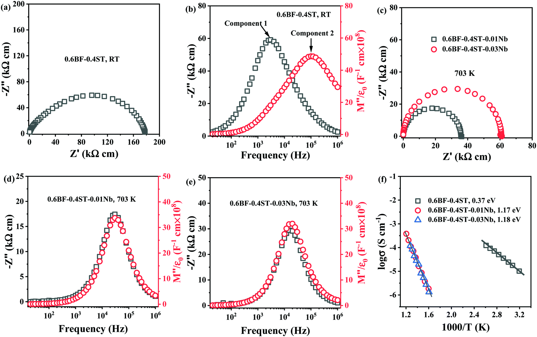 | ||
| Fig. 1 (a) Z* plots and (b) Z′′ and M′′ spectroscopic plots for 0.6BF–0.4ST ceramics at RT; (c) Z* plots for 0.6BF–0.4ST–0.01Nb and 0.03Nb ceramics; (d) and (e) Z′′ and M′′ spectroscopic plots for 0.6BF–0.4ST–0.01Nb and 0.03Nb ceramics at 703 K, respectively; (f) Arrhenius plots of bulk conductivity extracted from M′′ spectra. | ||
For 1 and 3% Nb doped 0.6BF–0.4ST, ceramics are too resistive to measure by impedance spectroscopy at RT and higher temperatures are required to obtain useful data. The Z* plots and Z′′, M′′ spectra for these samples at 703 K are shown in Fig. 1c–e. The most obvious difference in the data is the presence of a single arc in the Z* data, Fig. 1c and a single Z′′ and M′′ Debye peak that occurs at the same frequency, Fig. 1d and e. The FWHM of these peaks are ∼1.2 orders of magnitude, closer to the 1.14 decades for an ideal Debye response. The data are analysed using a single parallel RC element associated with a bulk response and clearly shows that 1–3% Nb doping produces a dramatic increase in electrical resistivity and improves the electrical homogeneity of the ceramics. An Arrhenius plot of the bulk conductivity (extracted from M′′ spectra) for all ceramics in this series is given in Fig. 1f and shows that Nb doped ceramics are excellent dielectrics with bulk conductivity <25 μS cm−1 at 703 K in contrast to undoped ceramics with a bulk conductivity that exceed 1 μS cm−1 at RT. In addition to the decrease in conductivity, there is a dramatic increase in the Ea associated with the bulk conductivity from ∼0.37 to ∼1.18 eV. This clearly indicates a change in the mechanism. ∼0.4 eV is consistent with p-type electronic conduction reported in undoped BF and suggests the presence of mixed oxidation states of Fe3+ and Fe4+ ions.45 The band gap of BF is reported to be ∼2.09 to 2.32![[thin space (1/6-em)]](https://www.rsc.org/images/entities/char_2009.gif) eV whereas for ST it is ∼3.2 eV.47,48 Although the exact band gap of BF–ST in this study is unknown, based on the end-members, an Ea of ∼1.2 eV is reasonably close to half the optical band gap, suggesting that the electronic conduction for the Nb-containing ceramics is close to the intrinsic (band gap) mechanism and beneficial for BDS.49,50 We conclude therefore, that p-type conduction mechanism has been successfully suppressed by Nb doping in BF–ST in accordance with eqn (3).
eV whereas for ST it is ∼3.2 eV.47,48 Although the exact band gap of BF–ST in this study is unknown, based on the end-members, an Ea of ∼1.2 eV is reasonably close to half the optical band gap, suggesting that the electronic conduction for the Nb-containing ceramics is close to the intrinsic (band gap) mechanism and beneficial for BDS.49,50 We conclude therefore, that p-type conduction mechanism has been successfully suppressed by Nb doping in BF–ST in accordance with eqn (3).
2.2. The role of sintering atmosphere on electrical conductivity
To establish the role of sintering atmosphere, preliminary studies were performed on 0.54–0.4ST–0.06BMN compositions without Nb doping (Section 2.3). Stoichiometric 5–6% BMN in BF–BaTiO3 (BT), had been proved successful in promoting chemical homogeneity and increasing the resistivity in previous studies31,32 and thus was considered a suitable initial concentration for investigation in this section.Impedance data for 0.54BF–0.4ST–0.06BMN ceramics sintered in air and N2 are shown in Fig. 2. Air sintered ceramics are leaky dielectrics at RT with a broadened and non-ideal arc in Z* with a total resistivity of ∼4 MΩ cm, Fig. 2a. The Z′′ spectrum displays a single, resistive element (component 1), R1 ∼ 3.5 MΩ cm and C1 ∼ 2.3 × 10⁻¹⁰ F cm−1 whereas the M′′ data shows the presence of a second element (component 2) that is more conductive, R2 ∼ 72 kΩ cm and C2 ∼ 1.1 × 10⁻¹⁰ F cm−1 and evidence for a third (yet more conductive) element with a peak maximum >1 MHz, Fig. 2b. These ceramics are clearly electrically heterogeneous with resistive and conductive components. The M′′ spectrum for component 2 has a bulk-related C value and an Arrhenius plot of the conductivity (1/R2) for this component is given in Fig. 2c and shows an Ea of ∼0.4 eV. This is consistent with the p-type mechanism obtained for 0.6BF–0.4ST ceramics, Fig. 1f.
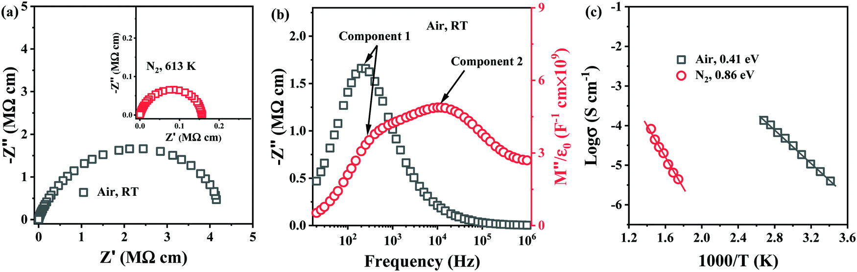 | ||
| Fig. 2 (a) Z* plots of the air sintered 0.54BF–0.4ST–0.06BMN ceramic at RT and the N2 sintered ceramic at 613 K as inserted, respectively; (b) Z′′ and M′′ spectroscopic plots at RT of the ceramic sintered in air; (c) the Arrhenius plots of conductivity extracted from M′′ plots for ceramics sintered in air and N2. | ||
In contrast, ceramics sintered in N2 are electrically insulating at RT and useful impedance data could only be obtained at >573 K. A Z* plot for a sample measured at 613 K is shown in Fig. 2a and displays a single, near ideal arc with a total resistivity of ∼0.16 MΩ cm. Z′′, M′′ spectra (not shown) displayed a single Debye peak with a maximum at the same frequency with C ∼ 1 × 10⁻¹⁰ F cm−1, confirming a bulk-type response. Processing in N2 dramatically improves the electrical homogeneity of the ceramics and suppresses the conductivity. An Arrhenius plot of the conductivity associated with the M′′ data is shown in Fig. 2c and displays much lower conductivity compared to air-fired ceramics with Ea ∼ 0.86 eV. Processing in N2 therefore, suppresses p-type conductivity but 0.54BF–0.4ST–0.06BMN ceramics are ∼one order of magnitude more conductive than Nb-containing 0.6BF–0.4ST ceramics at ∼623 K (1000/T = 1.6), Fig. 1f. This suggests that Nb-doping is more effective at suppressing p-type conductivity than processing in N2.
2.3. Nb doping in 0.54BF–0.4ST–0.06BMN–xNb (BF–ST–BMN–xNb) ceramics
X-ray diffraction (XRD) patterns of BF–ST–BMN–xNb (x = 0, 0.01, 0.02, 0.03, 0.04 and 0.05) are shown in Fig. 3a. The ionic radii of Nb5+ ions in 6-fold coordination is 0.64 Å and larger than the average for the B-site ions (0.625 Å) (Ti4+, 0.605 Å and Fe3+ high spin, 0.645 Å) for which it substitutes.51 Thus, peaks shift to lower 2θ as the Nb content increases but for x > 0.03, the solid solubility is breached and additional secondary peaks are observed. Backscattered Electron (BSE) images of polished surfaces of the BF–ST–BMN–xNb ceramics are presented in Fig. S1 (ESI†) which present polygonal grains <3 μm diameter with minimal porosity concomitant with relative density (ρr) >95%. Core–shell grains are observed in x = 0 with most grains displaying bright, BF-rich cores and dark, ST-rich shells. The presence of the core–shell microstructure in some grains in the Nb doped ceramics is confirmed by transmission electron microscopy (TEM), as displayed in Fig. 3b and Fig. S2 (ESI†). Consistent with XRD patterns (Fig. 3a), secondary phases appear in the ceramics for x > 0.03. The detailed quantitative data for each microstructural feature observed in x = 0.05 are listed in Table S1 (ESI†).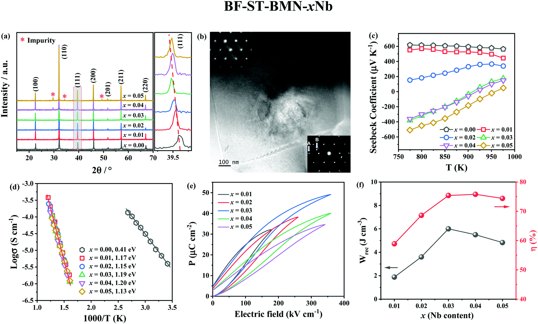 | ||
| Fig. 3 (a) XRD patterns, (b) TEM image obtained from x = 0.03, (c) Seebeck coefficients, (d) Arrhenius plots of conductivity obtained from M′′ peaks, (e) unipolar P–E loops under Emax, and (f) the energy storage properties, Wrec and η of BF–ST–BMN–xNb. | ||
The appearance of a core–shell microstructure results from microchemical segregation, driven by immiscibility, into Bi, Fe and Sr, Ti rich regions during slow-cooling from sintering.31,32,37 Although the microstructure arises from chemical heterogeneity, electrical homogeneity and low electrical conductivity have been demonstrated in previous studies through the use of dopants which modifies the defect chemistry of the core and shell such that they have similar resistivity based on impedance spectroscopy data.19 The elimination of conducting cores through electrical homogeneity enhances BDS and facilitates the fabrication of thinner dielectric layers suitable for MLCCs which do not short circuit under large applied field (>500 kV cm−1).19
The Seebeck coefficient (S) of BF–ST–BMN–xNb ceramics as a function of temperature is shown in Fig. 3c. The positive S for x ≤ 0.02 indicates p-type conduction but the magnitude of S becomes smaller as x increases, presumably due to a decrease in n.52 For x ≥ 0.03, S changes from positive to mixed negative and positive as a function of temperature, indicating a shift from p- to n-type conduction.53 Typical Z* plots and combined Z′′ and M′′ spectroscopic plots at 703 K of BF–ST–BMN–xNb ceramics are provided in Fig. S3a and b (ESI†). For x > 0 compositions, only one semicircle is observed in the Z* plot (Fig. S3a, ESI†), with a single Debye peak in both Z′′ and M′′ spectroscopic plots located at the same frequency (Fig. S3b, ESI†), indicating that all Nb doped ceramics are electrically homogeneous with only one parallel RC element.21 The total electrical resistivity of the Nb doped ceramics is several orders of magnitude higher than undoped. The absence of a semicircle/peak in the impedance data between 12 and 273 K (Fig. S3c and d, ESI†) provides strong evidence that there are no high conductivity regions in the Nb doped samples. The incline in M′′ is not a conductive component but is due to relaxor-type behavior, as shown in Fig. S4 (ESI†). Nb Doping is therefore effective at suppressing the p-type conductivity and increasing the electrical homogeneity of BF–ST–BMN. The Ea increases from ∼0.41 eV for x = 0 to ∼1.20 eV for x = 0.04 and eventually drops to ∼1.13 eV for x = 0.05 (Fig. 3d), indicating near intrinsic behaviour (band gap conduction) at x = 0.03 and 0.04, which is conducive to high BDS.49,50
The unipolar PE loops at maximum electric fields (Emax) of BF–ST–BMN–xNb (x = 0.01, 0.02, 0.03, 0.04, 0.05) are shown in Fig. 3e. x = 0 is too conductive to be measured, however, Emax is significantly enhanced for x > 0 in agreement with impedance data (Fig. S3, ESI†). The calculated energy storage properties are plotted in Fig. 3f, with maximum Wrec = 6 J cm−3 and η = 74.6% at 360 kV cm−1 for x = 0.03.
2.4. Variation of BMN with fixed Nb concentration (3%)
XRD patterns (Fig. 4a) reveal the unit cell volume of (0.6 − y)BF–0.4ST–0.03Nb–yBMN (BF–ST–Nb–yBMN) expands (peaks shift to the lower 2θ angles) with increasing BMN content since the average ionic radii of Mg2/3Nb1/3 in 6-fold coordination (0.693 Å) is larger than Fe3+ (high spin, 0.645 Å).54 BSE images acquired from BF–ST–Nb–yBMN (y = 0.02, 0.04, 0.06, 0.08, 0.10 and 0.12) ceramics are shown in Fig. S5 (ESI†). A core–shell microstructure is observed in all samples inside grains whose average grain size remains ∼3 μm, irrespective of BMN concentration. For y = 0.10 and 0.12, Bi-rich secondary phases are observed.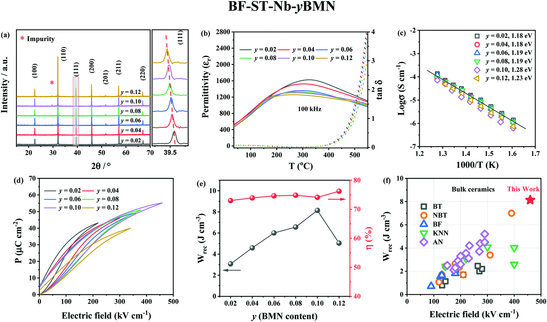 | ||
| Fig. 4 (a) The XRD patterns, (b) temperature dependent dielectric permittivity (εrvs. T) and loss (tanδ vs. T) data at 100 kHz, (c) Arrhenius plots of conductivity obtained from M′′ peaks, (d) unipolar P–E loops under Emax and (e) energy storage properties, Wrec and η for BF–ST–Nb–yBMN (y = 0.02, 0.04, 0.06, 0.08, 0.10 and 0.12). (f) A comparison of Wrec for y = 0.10 in this work with other lead-free bulk ceramics.11,12,55–89 | ||
ε
r and tanδ vs. temperature for BF–ST–Nb–yBMN ceramics at 100 kHz (Fig. 4b) show all compositions exhibit a broad εr maximum (εmax) which is frequency dependent (Fig. S6, ESI†), consistent with relaxor behaviour. εmax decreases and broadens with increasing BMN concentration. The Z* plots obtained from the ceramics at 703 K exhibit a single semicircle for each composition (Fig. S7a, ESI†) and co-incident Debye peaks in Z′′ and M′′ spectroscopic plots (Fig. S7b, ESI†). All data can be modelled on a single parallel RC element where bulk-type behavior dominates and therefore samples remain electrically homogeneous.21 With increasing BMN concentration, ceramics become more resistive with a small increase in Ea (Fig. 4c), suggesting potential further enhancement in BDS.
W rec and η for BF–ST–Nb–yBMN (y = 0.02, 0.04, 0.06, 0.08, 0.10 and 0.12) ceramics extrapolated from unipolar P–E loops under Emax are shown in Fig. 4d and e. The substitution of BMN leads to slimmer and relaxor-like P–E loops with higher η and higher BDS. Wrec reaches a maximum of 8.2 J cm−3 at 460 kV cm−1 with η of 74.1% for y = 0.10, which is the highest Wrec reported to date for lead-free bulk ceramics (see Fig. 4f).11,12,55–89
2.5. Landau–Devonshire (LD) phenomenological theory
The dopant strategies discussed in Sections 2.1–2.4 are not only designed to optimise the BDS but also to decrease the correlation length of polar coupling without decreasing the average ionic polarisability per unit volume. In this manner, it is proposed that Pmax may be optimised. However, this simplistic crystallochemical concept has to date not been proven in the context of a phenomenological model. Therefore, Landau–Devonshire (LD) phenomenological theory was employed to explore the microscopic origin of polarisation under E in BF–ST–Nb–BMN ceramics.90,91A two-phase (rhombohedral and cubic, R + C) coexistence model is initially proposed in which the nano-polar regions (NPRs) with R structure are randomly nucleated and embedded in a C non-polar matrix, Fig. 5a. According to the local random field (LRF) model,92–95 the polar regions are oriented along different polarisation directions, are isotropic and macroscopically paraelectric (with zero macroscopic polarisation), in agreement with a superparaelectric model.96 The schematic picture of a three-dimensional (3D) Landau free-energy F(![[P with combining right harpoon above (vector)]](https://www.rsc.org/images/entities/i_char_0050_20d1.gif) ) profile of polarisation rotation for BF–ST–Nb–BMN is given in Fig. 5b. F() of rhombohedral (R), tetragonal (T) and orthorhombic (O) phases follows the sequence, R < T < O, indicating that R-phase is the only polar phase retained at RT at zero field. However, the energy barrier to polarisation rotation between 〈111〉R and 〈100〉T is small, as shown in the two-dimensional (2D) Landau free-energy curve, Fig. 5c, which suggests the polar phase may easily undergo polarisation rotation between 〈111〉 and 〈100〉 directions under an external E. The 2D F() curve of polarisation extension for BF–ST–Nb–BMN is shown in Fig. 5d, where a small energy barrier between the paraelectric (C) and ferroelectric (R) phases is found. With an external E, the F() of the relaxor is lowered, as shown in Fig. 5d, which indicates a large polarisation response is induced under a modest E. Consequently, the NPRs in BF–ST–Nb–BMN are easy to re-orientate and re-arrange in the direction of E, Fig. 5e, due to the small energy barriers associated with polarisation rotation and extension.97
) profile of polarisation rotation for BF–ST–Nb–BMN is given in Fig. 5b. F() of rhombohedral (R), tetragonal (T) and orthorhombic (O) phases follows the sequence, R < T < O, indicating that R-phase is the only polar phase retained at RT at zero field. However, the energy barrier to polarisation rotation between 〈111〉R and 〈100〉T is small, as shown in the two-dimensional (2D) Landau free-energy curve, Fig. 5c, which suggests the polar phase may easily undergo polarisation rotation between 〈111〉 and 〈100〉 directions under an external E. The 2D F() curve of polarisation extension for BF–ST–Nb–BMN is shown in Fig. 5d, where a small energy barrier between the paraelectric (C) and ferroelectric (R) phases is found. With an external E, the F() of the relaxor is lowered, as shown in Fig. 5d, which indicates a large polarisation response is induced under a modest E. Consequently, the NPRs in BF–ST–Nb–BMN are easy to re-orientate and re-arrange in the direction of E, Fig. 5e, due to the small energy barriers associated with polarisation rotation and extension.97
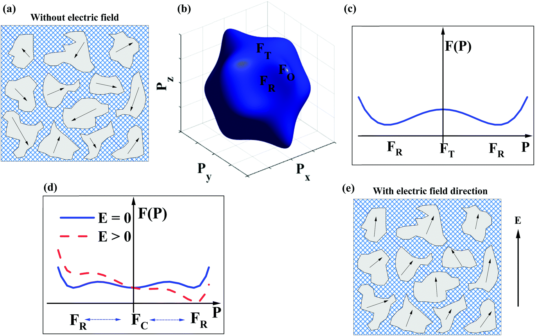 | ||
| Fig. 5 (a) 2D cartoon of polar (R) coexisting with a non-polar cubic (C) phase without an external E. (b) 3D Landau free-energy profile of polarisation rotation for different polarisations under the two-phase (R + C) coexistence condition. (c) 2D Landau free-energy curve between 〈111〉R and 〈100〉T polarisation directions. (d) 2D Landau free-energy curve of polarisation extension F() under the two-phase (R + C) coexistence conditions with and without an external E. (e) 2D cartoon for the NPRs with an external E in a given direction. | ||
According to the above, as E increases, Pmax for BF–ST–Nb–BMN is expected to keep increasing by both polarisation rotation and extension due to the small values of F(). As a result, provided a high BDS is maintained, a continuous increase of P with E is predicted leading to high Wrec and large η.
2.6. Multilayer ceramic capacitors
Sections 2.1–2.3 have systematically demonstrated how the resistivity and electrical homogeneity can be increased through Nb doping. Moreover, substituting BMN for BF (Section 2.4) in the formulation further disrupts long range polar order by introducing a wider spread of ion size and charge on the B-site without decreasing the average ionic polarisability of the solid solution. This has been shown by LD theory to maximise P in the direction of the applied field through polarisation extension and rotation (Section 2.5). In combination, these two effects have resulted in a highly resistive, electrically homogeneous, slim-looped relaxor with the potential of sustaining a high Pmax at high E without breakdown. In this section, we utilise a ceramic composition with the optimum Wrec, BF–ST–Nb–0.1BMN, and increase its BDS and thus Pmax through reduction in dielectric layer thickness, following the Gerson–Marshall relationship.98An SEM image and corresponding energy-dispersive spectroscopy (EDS) elemental maps acquired from a cross section of a multilayer are illustrated in Fig. S8 (ESI†). The thickness and active electrode area of one dielectric layer are ∼8 μm (Fig. S8, ESI†) and 5 mm2, respectively. The interface between the Pt electrode and BF–ST–Nb–0.1BMN ceramic is characterised using (scanning) transmission electron microscopy ((S)TEM) with images, electron diffraction patterns and associated EDS maps shown in Fig. 6(a–f). According to the selected area diffraction (SAD) patterns in Fig. 6b and c, the {011} atomic planes of the ceramic grain displayed in Fig. 6a are ∼7° off parallel to Pt{011} which is considered as a nominally random arrangement. However, a coherent 10–20 nm intermediate layer is observed at the surface of Pt. We propose that Bi3+ in the BF-based ceramic is reduced by residual carbon from the binder at the Pt/dielectric interface and forms an alloy with the Pt.99 The EDS maps in Fig. 6e confirm the presence of Bi in the intermediate layer. In addition, discrete Bi–Pt phases, marked by α and β in Fig. 6d are observed, the former of which based on Fig. 6e and f, is indexed as Bi2Pt.
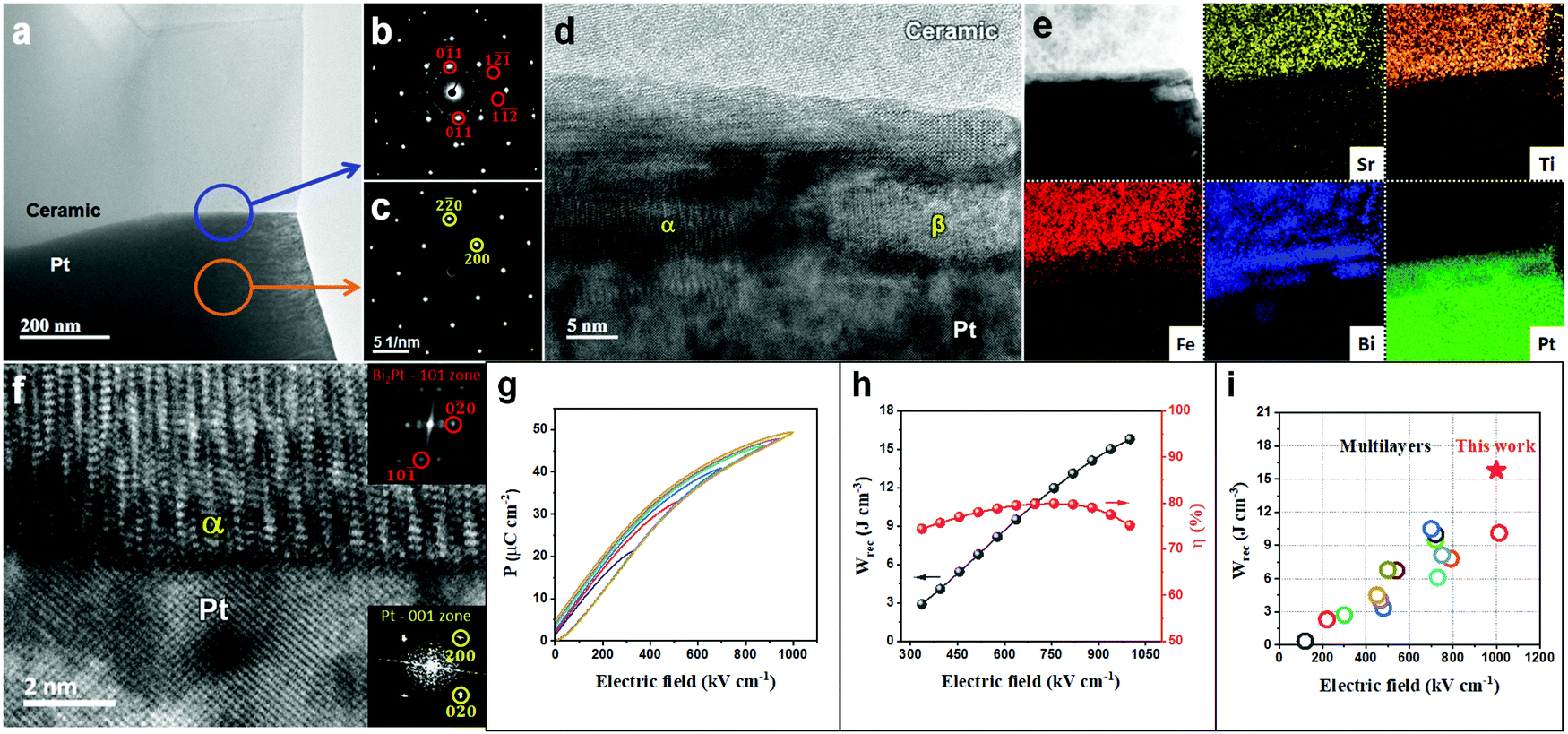 | ||
| Fig. 6 (a) TEM micrograph obtained from an interface between a BF–ST–Nb–0.1BMN grain and a Pt grain (electrode). Here the Pt grain is close to its [001] zone axis and the BF–ST–Nb–0.1BMN grain is ∼10° off from its [311] zone axis. (b) SAD pattern obtained from the area marked by a blue circle shown on (a) i.e. interface between BF–ST–Nb–0.1BMN and Pt. Here, few reflections related to BF–ST–Nb–0.1BMN are marked by red circles. (c) SAD pattern obtained from the area marked by an orange circle shown on (a), i.e. Pt. (d) High resolution TEM micrograph obtained from the interface between ceramic and Pt shown in (a). Here different phases (e.g. α and β) are observed at the surface of Pt. (e) A bright-field STEM image and corresponding chemical EDS elemental maps obtained from the interface between ceramic and Pt shown in (a). (f) A bright-field STEM image obtained from the interface between Pt and α shown in (d). (g) Unipolar P–E loops. (h) The energy storage properties, Wrec and η, for BF–ST–Nb–0.1BMN multilayer. (i) A comparison for Wrec of the multilayer in this work with other lead-free multilayers reported in ref. 10, 12, 13, 21, 56 and 100–109. | ||
The unipolar P–E loops and energy storage properties for the BF–ST–Nb–0.1BMN multilayer are shown in Fig. 6g–i. With increasing E, Wrec increases until breakdown at >1000 kV cm−1, thereby illustrating the enhancement in BDS in accordance with the Gerson–Marshall relationship.98 The multilayer achieved the highest recorded Wrec of 15.8 J cm−3 with η = 75.2% for random polycrystalline lead-free MLCCs. Given the high BDS, it is not clear how the formation of the Bi–Pt alloy affects the high field electrical properties but it is likely that reduction will locally affect Pmax in the vicinity of the interface by decreasing the concentration of the Bi-rich phase. Whether this also creates a local space charge layer, more conducting than the bulk of the dielectric within the multilayer, remains to be elucidated.
3. Conclusions
A systematic strategy to optimise BDS and Pmax in high energy density capacitors is presented. Nb doping increases resistivity by eliminating p-type leakage conduction and promotes electrical homogeneity whereas a third perovskite end-member, BMN, mainly promotes relaxor behaviour for which Landau–Devonshire theory predicts a large microscopic polarisation originating from its flat thermodynamic energy profile. This results in an increase in BDS and Pmax at high field to give Wrec = 8.2 J cm−3 at 460 kV cm−1 for BF–ST–0.03Nb–0.1BMN ceramics which facilitated a multilayer with 8 μm dielectric layer thickness with BDS > 1000 kV cm−1 and Wrec = 15.8 J cm−3. The multilayer showed evidence of interfacial reactions and Bi–Pt alloy formation which might, despite the very high BDS, have been deleterious to Wrec by decreasing Pmax.4. Experimental
BF–ST based systems, 0.6BiFeO3–0.4SrTiO3–xNb (x = 0, 0.01, 0.03), 0.54BiFeO3–0.4SrTiO3–0.06Bi(Mg2/3Nb1/3)O3–xNb (BF–ST–BMN–xNb, x = 0, 0.01, 0.02, 0.03, 0.04 and 0.05) and (0.6 − y)BiFeO3–0.4SrTiO3–0.03Nb–yBi(Mg2/3Nb1/3)O3, (BF–ST–Nb–yBMN, y = 0.02, 0.04, 0.06, 0.08, 0.10 and 0.12) ceramics were synthesised using analytical-grade raw chemicals of Bi2O3, Fe2O3, SrCO3, TiO2, MgO and Nb2O5 by a conventional solid state reaction method. Stoichiometric amounts of dry raw powders were weighed, and ball milled for 6 hours with Y2O3-stabilized ZrO2 grinding media in isopropanol. The mixed powders were calcined at 800 °C for 2 hours and then ball milled again for 6 hours prior to sintering. The final dry powders were uniaxially pressed into 8 mm diameter pellets then sintered at 1070–1100 °C for 3 hours in air or N2. The same dry powder was used to fabricate ceramic multilayers using an MTI MSK-AFA-II tape caster.21 A DEK 247 screen printer was employed to print Pt electrodes onto the tape, followed by stacking and hot-pressing at 80 °C for 20 min. Multilayers were sintered using the same procedure as for the bulk ceramics but with the addition of two more intermediate binder burnout steps (180 °C for 3 h and 300 °C for 3 h).X-ray diffraction (XRD) on ceramics was performed using a Bruker D2 phaser. The operating voltage and current were 40 kV and 30 mA, respectively. The polished surface morphology of ceramic samples was examined using a FEI Inspect F50 scanning electron microscope (SEM) with BSE and EDS detectors. Samples for (scanning) transmission electron microscopy ((S)TEM) were mechanically grounded to reach a thickness of ∼50 μm. Further polishing was conducted at liquid nitrogen temperature by Ar+ ion milling using a Gatan Precision Ion Polishing System PIPS (II). (S)TEM data were acquired with a JEOL JEM 2100F (JEOL, Tokyo, Japan) operated at 200 kV. Impedance spectroscopy (IS) data were collected using an Agilent E4980A (Agilent Technologies Inc., Palo-Alto, CA) from 20 Hz–2 MHz and from 12 to 873 K with an ac voltage of 100 mV. Resistivity of samples was obtained by fitting the experimental IS data using ZView software (Scribner Associates, Inc., Southern Pines, NC). The temperature dependence of the dielectric properties (permittivity and tanδ) were measured using an Agilent 4184A precision LCR meter from room temperature (RT) to 550 °C at 1, 10, 100, 250 kHz and 1 MHz. IS and LCR data were corrected by a geometric factor (thickness/surface area). For ferroelectric polarisation–field (P–E) loops measurements, ceramics were ground to a thickness of ∼0.15 mm and then gold sputtered. Bipolar P–E loops were obtained using an aixACCT TF 2000E ferroelectric tester at 1 Hz.
Conflicts of interest
There are no conflicts of interest to declare.Acknowledgements
We acknowledge the Henry Royce Institute for Advanced Materials, funded through EPSRC grants EP/R00661X/1, EP/S019367/1, EP/P02470X/1 and EP/P025285/1, for the financial support at The University of Sheffield. We thank the EPSRC for funding aspects of this work via ‘SUBStitution and Sustainability in Functional Materials and Devices, SUBST’ (EP/L017563/1), ‘SYnthesizing 3D METAmaterials for RF, microwave and THz applications, SYMETA’ (EP/N010493/1), ‘Framework for designing Piezoelectric Transformer power supplies, FPeT’ (EP/P015859/1) and support provided by the Functional Materials and Devices group at The University of Sheffield.References
- E. Karden, S. Ploumen, B. Fricke, T. Miller and K. Snyder, J. Power Sources, 2007, 168, 2–11 CrossRef.
- I. Hadjipaschalis, A. Poullikkas and V. Efthimiou, Renewable Sustainable Energy Rev., 2009, 13, 1513–1522 CrossRef.
- H. Pan, F. Li, Y. Liu, Q. Zhang, M. Wang, S. Lan, Y. Zheng, J. Ma, L. Gu, Y. Shen, P. Yu, S. Zhang, L. Chen, Y. Lin and C. Nan, Science, 2019, 365, 578–582 CrossRef PubMed.
- H. Qi, R. Zuo, A. Xie, A. Tian, J. Fu, Y. Zhang and S. Zhang, Adv. Funct. Mater., 2019, 29, 1903877 CrossRef.
- J. Li, Z. Shen, X. Chen, S. Yang, W. Zhou, M. Wang, L. Wang, Q. Kou, Y. Liu, Q. Li, Z. Xu, Y. Chang, S. Zhang and F. Li, Nat. Mater., 2020, 19, 999–1005 CrossRef PubMed.
- H. Palneedi, M. Peddigari, G.-T. Hwang, D.-Y. Jeong and J. Ryu, Adv. Funct. Mater., 2018, 28, 1803665 CrossRef.
- X. Hao, J. Adv. Dielectr., 2013, 03, 1330001 CrossRef.
- Z. Yu, S. Jiao, S. Li, X. Chen, W.-L. Song, T. Teng, J. Tu, H.-S. Chen, G. Zhang and D.-N. Fang, Adv. Funct. Mater., 2019, 29, 1806799 CrossRef.
- X. Zhang, S. Jiao, J. Tu, W.-L. Song, X. Xiao, S. Li, M. Wang, H. Lei, D. Tian, H. Chen and D. Fang, Energy Environ. Sci., 2019, 12, 1918–1927 RSC.
- H. Ogihara, C. A. Randall and S. Trolier-McKinstry, J. Am. Ceram. Soc., 2009, 92, 1719–1724 CrossRef.
- H. Qi and R. Zuo, J. Mater. Chem. A, 2019, 7, 3971–3978 RSC.
- D. Wang, Z. Fan, D. Zhou, A. Khesro, S. Murakami, A. Feteira, Q. Zhao, X. Tan and I. M. Reaney, J. Mater. Chem. A, 2018, 6, 4133–4144 RSC.
- P. Zhao, H. Wang, L. Wu, L. Chen, Z. Cai, L. Li and X. Wang, Adv. Energy Mater., 2019, 9, 1803048 CrossRef.
- R. Ma, B. Cui, M. Shangguan, S. Wang, Y. Wang, Z. Chang and Y. Wang, J. Alloys Compd., 2017, 690, 438–445 CrossRef CAS.
- F. Inam, H. Yan, D. D. Jayaseelan, T. Peijs and M. J. Reece, J. Eur. Ceram. Soc., 2010, 30, 153–157 CrossRef CAS.
- Z. Song, H. Liu, S. Zhang, Z. Wang, Y. Shi, H. Hao, M. Cao, Z. Yao and Z. Yu, J. Eur. Ceram. Soc., 2014, 34, 1209–1217 CrossRef CAS.
- H. Y. Lee, K. H. Cho and H.-D. Nam, Ferroelectrics, 2006, 334, 165–169 CrossRef CAS.
- X. Su, B. C. Riggs, M. Tomozawa, J. K. Nelson and D. B. Chrisey, J. Mater. Chem. A, 2014, 2, 18087–18096 RSC.
- L. Meng, L. Zheng, L. Cheng, G. Li, L. Huang, Y. Gu and F. Zhang, J. Mater. Chem., 2011, 21, 11418 RSC.
- L.-M. Wang, Proceedings of the 25th international conference on microelectronics, 2006, pp. 576–579.
- G. Wang, J. Li, X. Zhang, Z. Fan, F. Yang, A. Feteira, D. Zhou, D. C. Sinclair, T. Ma, X. Tan, D. Wang and I. M. Reaney, Energy Environ. Sci., 2019, 12, 582–588 RSC.
- Y. H. Han, J. B. Appleby and D. M. Smyth, J. Am. Ceram. Soc., 1987, 70, 96–100 CrossRef CAS.
- I. Burn and G. H. Maher, J. Mater. Sci., 1975, 10, 633–640 CrossRef CAS.
- F. D. Morrison, D. C. Sinclair and A. R. West, J. Am. Ceram. Soc., 2001, 84, 474–476 CrossRef CAS.
- F. D. Morrison, D. C. Sinclair and A. R. West, J. Am. Ceram. Soc., 2001, 84, 531–538 CrossRef CAS.
- L. Li, M. Li, H. Zhang, I. M. Reaney and D. C. Sinclair, J. Mater. Chem. C, 2016, 4, 5779–5786 RSC.
- F. Yang, M. Li, L. Li, P. Wu, E. Pradal-Velázque and D. C. Sinclair, J. Mater. Chem. A, 2017, 5, 21658–21662 RSC.
- N. Liu, R. Liang, G. Zhang, Z. Zhou, S. Yan, X. Li and X. Dong, J. Mater. Chem. C, 2018, 6, 10415–10421 RSC.
- X.-S. Cao, Mater. Res. Express, 2019, 6, 076112 CrossRef CAS.
- D.-C. Jia, J.-H. Xu, H. Ke, W. Wang and Y. Zhou, J. Eur. Ceram. Soc., 2009, 29, 3099–3103 CrossRef CAS.
- S. Murakami, N. T. A. F. Ahmed, D. Wang, A. Feteira, D. C. Sinclair and I. M. Reaney, J. Eur. Ceram. Soc., 2018, 38, 4220–4231 CrossRef CAS.
- S. Murakami, D. Wang, A. Mostaed, A. Khesro, A. Feteira, D. C. Sinclair, Z. Fan, X. Tan and I. M. Reaney, J. Am. Ceram. Soc., 2018, 101, 5428–5442 CrossRef CAS.
- G. Wang, Z. Fan, S. Murakami, Z. Lu, D. A. Hall, D. C. Sinclair, A. Feteira, X. Tan, J. L. Jones, A. K. Kleppe, D. Wang and I. M. Reaney, J. Mater. Chem. A, 2019, 7, 21254–21263 RSC.
- Y. Li, M.-S. Cao, D.-W. Wang and J. Yuan, RSC Adv., 2015, 5, 77184–77191 RSC.
- Y. Li, W.-Q. Cao, J. Yuan, D.-W. Wang and M.-S. Cao, J. Mater. Chem. C, 2015, 3, 9276–9282 RSC.
- Z.-J. Li, Z.-L. Hou, W.-L. Song, X.-D. Liu, D.-W. Wang, J. Tang and X.-H. Shao, Mater. Lett., 2016, 175, 207–211 CrossRef CAS.
- D. Wang, G. Wang, S. Murakami, Z. Fan, A. Feteira, D. Zhou, S. Sun, Q. Zhao and I. M. Reaney, J. Adv. Dielectr., 2019, 08, 1830004 CrossRef.
- D. Wang, M. Wang, F. Liu, Y. Cui, Q. Zhao, H. Sun, H. Jin and M. Cao, Ceram. Int., 2015, 41, 8768–8772 CrossRef CAS.
- T. Rojac, A. Bencan, B. Malic, G. Tutuncu, J. L. Jones, J. E. Daniels, D. Damjanovic and D. J. Green, J. Am. Ceram. Soc., 2014, 97, 1993–2011 CrossRef CAS.
- L. Wang, R. Liang, Z. Zhou, M. Li, M. Gu, P. Wang and X. Dong, J. Eur. Ceram. Soc., 2019, 39, 4727–4734 CrossRef CAS.
- T. Correia, M. Stewart, A. Ellmore and K. Albertsen, Adv. Eng. Mater., 2017, 19, 1700019 CrossRef.
- M. Makarovic, A. Bencan, J. Walker, B. Malic and T. Rojac, J. Eur. Ceram. Soc., 2019, 39, 3693–3702 CrossRef CAS.
- S. Vura, P. S. Anil Kumar, A. Senyshyn and R. Ranjan, J. Magn. Magn. Mater., 2014, 365, 76–82 CrossRef CAS.
- N. Masó and A. R. West, Chem. Mater., 2012, 24, 2127–2132 CrossRef.
- M. Schrade, N. Masó, A. Perejón, L. A. Pérez-Maqueda and A. R. West, J. Mater. Chem. C, 2017, 5, 10077–10086 RSC.
- J. T. S. Irvine, D. C. Sinclair and A. R. West, Adv. Mater., 1990, 2, 132–138 CrossRef CAS.
- C. Wang, H. Qiu, T. Inoue and Q. Yao, Int. J. Hydrogen Energy, 2014, 39, 12507–12514 CrossRef CAS.
- P. S. V. Mocherla, C. Karthik, R. Ubic, M. S. Ramachandra Rao and C. Sudakar, Appl. Phys. Lett., 2013, 103, 022910 CrossRef.
- X. Qiao, D. Wu, F. Zhang, B. Chen, X. Ren, P. Liang, H. Du, X. Chao and Z. Yang, J. Mater. Chem. C, 2019, 7, 10514–10520 RSC.
- L. Yang, X. Kong, F. Li, H. Hao, Z. Cheng, H. Liu, J.-F. Li and S. Zhang, Prog. Mater. Sci., 2019, 102, 72–108 CrossRef CAS.
- R. D. Shannon, Acta Crystallogr., Sect. A: Cryst. Phys., Diffr., Theor. Gen. Crystallogr., 1976, 32, 751–767 CrossRef.
- Z. Lu, H. Zhang, W. Lei, D. C. Sinclair and I. M. Reaney, Chem. Mater., 2016, 28, 925–935 CrossRef CAS.
- G. C. Dannangoda, C. Key, M. Sumets and K. S. Martirosyan, J. Electron. Mater., 2018, 47, 5800–5809 CrossRef CAS.
- R. D. Shannon, Acta Crystallogr., 1976, A32, 751–767 CrossRef CAS.
- L. Zhao, J. Gao, Q. Liu, S. Zhang and J. F. Li, ACS Appl. Mater. Interfaces, 2018, 10, 819–826 CrossRef PubMed.
- W.-B. Li, D. Zhou, R. Xu, L.-X. Pang and I. M. Reaney, ACS Appl. Energy Mater., 2018, 1, 5016–5023 CrossRef.
- D. Wang, Z. Fan, W. Li, D. Zhou, A. Feteira, G. Wang, S. Murakami, S. Sun, Q. Zhao, X. Tan and I. M. Reaney, ACS Appl. Energy Mater., 2018, 1, 4403–4412 CrossRef.
- Y. Pu, L. Zhang, Y. Cui and M. Chen, ACS Sustainable Chem. Eng., 2018, 6, 6102–6109 CrossRef CAS.
- L. Zhao, Q. Liu, J. Gao, S. Zhang and J. F. Li, Adv. Mater., 2017, 29, 1701824 CrossRef.
- W.-B. Li, D. Zhou and L.-X. Pang, Appl. Phys. Lett., 2017, 110, 132902 CrossRef.
- K. Han, N. Luo, Y. Jing, X. Wang, B. Peng, L. Liu, C. Hu, H. Zhou, Y. Wei, X. Chen and Q. Feng, Ceram. Int., 2019, 45, 5559–5565 CrossRef CAS.
- C. Cui, Y. Pu, Z. Gao, J. Wan, Y. Guo, C. Hui, Y. Wang and Y. Cui, J. Alloys Compd., 2017, 711, 319–326 CrossRef CAS.
- J. Gao, Y. Zhang, L. Zhao, K.-Y. Lee, Q. Liu, A. Studer, M. Hinterstein, S. Zhang and J.-F. Li, J. Mater. Chem. A, 2019, 7, 2225–2232 RSC.
- W.-B. Li, D. Zhou, L.-X. Pang, R. Xu and H.-H. Guo, J. Mater. Chem. A, 2017, 5, 19607–19612 RSC.
- N. Luo, K. Han, F. Zhuo, C. Xu, G. Zhang, L. Liu, X. Chen, C. Hu, H. Zhou and Y. Wei, J. Mater. Chem. A, 2019, 7, 14118–14128 RSC.
- T. Shao, H. Du, H. Ma, S. Qu, J. Wang, J. Wang, X. Wei and Z. Xu, J. Mater. Chem. A, 2017, 5, 554–563 RSC.
- Y. Tian, L. Jin, Q. Hu, K. Yu, Y. Zhuang, G. Viola, I. Abrahams, Z. Xu, X. Wei and H. Yan, J. Mater. Chem. A, 2019, 7, 834–842 RSC.
- Y. Tian, L. Jin, H. Zhang, Z. Xu, X. Wei, E. D. Politova, S. Y. Stefanovich, N. V. Tarakina, I. Abrahams and H. Yan, J. Mater. Chem. A, 2016, 4, 17279–17287 RSC.
- Y. Tian, L. Jin, H. Zhang, Z. Xu, X. Wei, G. Viola, I. Abrahams and H. Yan, J. Mater. Chem. A, 2017, 5, 17525–17531 RSC.
- L. Yang, X. Kong, Z. Cheng and S. Zhang, J. Mater. Chem. A, 2019, 7, 8573–8580 RSC.
- Z. Yang, H. Du, S. Qu, Y. Hou, H. Ma, J. Wang, J. Wang, X. Wei and Z. Xu, J. Mater. Chem. A, 2016, 4, 13778–13785 RSC.
- J. Yin, Y. Zhang, X. Lv and J. Wu, J. Mater. Chem. A, 2018, 6, 9823–9832 RSC.
- S. Li, H. Nie, G. Wang, C. Xu, N. Liu, M. Zhou, F. Cao and X. Dong, J. Mater. Chem. C, 2019, 7, 1551–1560 RSC.
- N. Luo, K. Han, F. Zhuo, L. Liu, X. Chen, B. Peng, X. Wang, Q. Feng and Y. Wei, J. Mater. Chem. C, 2019, 7, 4999–5008 RSC.
- Z. Pan, D. Hu, Y. Zhang, J. Liu, B. Shen and J. Zhai, J. Mater. Chem. C, 2019, 7, 4072–4078 RSC.
- Q. Yuan, F. Yao, Y. Wang, R. Ma and H. Wang, J. Mater. Chem. C, 2017, 5, 9552–9558 RSC.
- L. Zhao, Q. Liu, S. Zhang and J.-F. Li, J. Mater. Chem. C, 2016, 4, 8380–8384 RSC.
- K. Han, N. Luo, S. Mao, F. Zhuo, X. Chen, L. Liu, C. Hu, H. Zhou, X. Wang and Y. Wei, J. Materiomics, 2019, 5, 597–605 CrossRef.
- N. Luo, K. Han, L. Liu, B. Peng, X. Wang, C. Hu, H. Zhou, Q. Feng, X. Chen and Y. Wei, J. Am. Ceram. Soc., 2019, 102, 4640–4647 CrossRef CAS.
- B. Qu, H. Du, Z. Yang and Q. Liu, J. Am. Ceram. Soc., 2017, 100, 1517–1526 CrossRef CAS.
- T. Wang, L. Jin, C. Li, Q. Hu, X. Wei and D. Lupascu, J. Am. Ceram. Soc., 2015, 98, 559–566 CrossRef CAS.
- D. Zheng, R. Zuo, D. Zhang, Y. Li and X. Tan, J. Am. Ceram. Soc., 2015, 98, 2692–2695 CrossRef CAS.
- D. Zheng and R. Zuo, J. Eur. Ceram. Soc., 2017, 37, 413–418 CrossRef CAS.
- T. Wang, L. Jin, Y. Tian, L. Shu, Q. Hu and X. Wei, Mater. Lett., 2014, 137, 79–81 CrossRef CAS.
- F. Li, J. Zhai, B. Shen, X. Liu and H. Zeng, Mater. Res. Lett., 2018, 6, 345–352 CrossRef CAS.
- J. Wu, A. Mahajan, L. Riekehr, H. Zhang, B. Yang, N. Meng, Z. Zhang and H. Yan, Nano Energy, 2018, 50, 723–732 CrossRef CAS.
- Z. Yang, F. Gao, H. Du, L. Jin, L. Yan, Q. Hu, Y. Yu, S. Qu, X. Wei, Z. Xu and Y.-J. Wang, Nano Energy, 2019, 58, 768–777 CrossRef CAS.
- B. Qu, H. Du, Z. Yang, Q. Liu and T. Liu, RSC Adv., 2016, 6, 34381–34389 RSC.
- L. Wu, X. Wang and L. Li, RSC Adv., 2016, 6, 14273–14282 RSC.
- S.-Y. Liu, E. Zhang, S. Liu, D.-J. Li, Y. Li, Y. Liu, Y. Shen, S. Wang and C. Landis, J. Am. Ceram. Soc., 2016, 99, 3336–3342 CrossRef CAS.
- S. Y. Liu, Y. Meng, S. Liu, D. J. Li, Y. Li, Y. Liu, Y. Shen and S. Wang, Phys. Chem. Chem. Phys., 2017, 19, 22190–22196 RSC.
- R. Pirc and R. Blinc, Phys. Rev. B: Condens. Matter Mater. Phys., 1999, 60, 13470–13478 CrossRef CAS.
- S. Tinte, B. P. Burton, E. Cockayne and U. V. Waghmare, Phys. Rev. Lett., 2006, 97, 137601 CrossRef.
- V. V. Westphal, W. Kleemann and M. D. Glinchuk, Phys. Rev. Lett., 1992, 68, 847–850 CrossRef CAS PubMed.
- B. Burton, E. Cockayne and U. Waghmare, Phys. Rev. B: Condens. Matter Mater. Phys., 2005, 72, 064113 CrossRef.
- L. E. Cross, Ferroelectrics, 1987, 76, 241–267 CrossRef CAS.
- Y. Xi, C. Zhili and L. E. Cross, J. Appl. Phys., 1983, 54, 3399–3403 CrossRef.
- R. Gerson and T. C. Marshall, J. Appl. Phys., 1959, 30, 1650–1653 CrossRef CAS.
- G. Wang, Z. Lu, H. Yang, H. Ji, A. Mostaed, L. Li, Y. Wei, A. Feteira, S. Sun, D. C. Sinclair, D. Wang and I. M. Reaney, J. Mater. Chem. A, 2020, 8, 11414–11423 RSC.
- W.-B. Li, D. Zhou, R. Xu, D.-W. Wang, J.-Z. Su, L.-X. Pang, W.-F. Liu and G.-H. Chen, ACS Appl. Energy Mater., 2019, 2, 5499–5506 CrossRef CAS.
- Y. Gao, H. Liu, Z. Yao, H. Hao, Z. Yu and M. Cao, Ceram. Int., 2017, 43, 8418–8423 CrossRef CAS.
- L. Chen, Y. Li, Q. Zhang and X. Hao, Ceram. Int., 2016, 42, 12537–12542 CrossRef CAS.
- Z. Cai, C. Zhu, H. Wang, P. Zhao, L. Chen, L. Li and X. Wang, J. Mater. Chem. A, 2019, 7, 14575–14582 RSC.
- G. Wang, Z. Lu, J. Li, H. Ji, H. Yang, L. Li, S. Sun, A. Feteira, H. Yang, R. Zuo, D. Wang and I. M. Reaney, J. Eur. Ceram. Soc., 2020, 40, 1779–1783 CrossRef CAS.
- L. Chen, N. Sun, Y. Li, Q. zhang, L. Zhang and X. Hao, J. Am. Ceram. Soc., 2018, 101, 2313–2320 CrossRef CAS.
- L. Chen, H. Wang, P. Zhao, C. Zhu, Z. Cai, Z. Cen, L. Li and X. Wang, J. Am. Ceram. Soc., 2019, 102, 4178–4187 CrossRef CAS.
- J. Li, F. Li, Z. Xu and S. Zhang, Adv. Mater., 2018, 30, 1802155 CrossRef.
- Z. Cai, H. Wang, P. Zhao, L. Chen, C. Zhu, K. Hui, L. Li and X. Wang, Appl. Phys. Lett., 2019, 115, 023901 CrossRef.
- W. Jia, Y. Hou, M. Zheng, Y. Xu, X. Yu, M. Zhu, K. Yang, H. Cheng, S. Sun and J. Xing, J. Am. Ceram. Soc., 2018, 101, 3468–3479 CrossRef CAS.
Footnotes |
| † Electronic supplementary information (ESI) available. See DOI: 10.1039/d0ee02104k |
| ‡ Z. Lu, G. Wang, W. Bao and J. Li contributed equally to this work. |
| This journal is © The Royal Society of Chemistry 2020 |