
 Open Access Article
 This Open Access Article is licensed under a Creative Commons Attribution-Non Commercial 3.0 Unported Licence
Environmental impacts of III–V/silicon photovoltaics: life cycle assessment and guidance for sustainable manufacturing†
Carlos F.
Blanco
 *a,
Stefano
Cucurachi
a,
Frank
Dimroth
b,
Jeroen B.
Guinée
a,
Willie J. G. M.
Peijnenburg
ac and
Martina G.
Vijver
a
*a,
Stefano
Cucurachi
a,
Frank
Dimroth
b,
Jeroen B.
Guinée
a,
Willie J. G. M.
Peijnenburg
ac and
Martina G.
Vijver
a
aInstitute of Environmental Sciences (CML), Leiden University, Box 9518, 2300 RA Leiden, The Netherlands. E-mail: c.f.blanco@cml.leidenuniv.nl
bFraunhofer Institute for Solar Energy Systems, Heidenhofstr. 2, 79110 Freiburg, Germany
cNational Institute of Public Health and the Environment (RIVM), Center for Safety of Substances and Products, P. O. Box 1, 3720 BA Bilthoven, The Netherlands
First published on 6th October 2020
Abstract
Multijunction III–V/silicon photovoltaic cells (III–V/Si), which have achieved record conversion efficiencies, are now looking as a promising option to replace conventional silicon cells in future PV markets. As efforts to increase efficiency and reduce cost are gaining important traction, it is of equal importance to understand whether the manufacturing methods and materials used in these cells introduce undesired environmental trade-offs. We investigate this for two state-of-the-art III–V/Si cell design concepts using life cycle assessment. Considering that the proposed III–V/Si technologies are still at an early research and design stage, we use probabilistic methods to account for uncertainties in the extrapolation from lab-based data to more industrially relevant processes. Our study shows that even at this early stage and in light of potential uncertainties, the III–V/Si PV systems are well positioned to outperform the incumbent silicon PV systems in terms of life-cycle environmental impacts. We also identify key elements for more sustainable choices in the III–V/Si design and manufacturing methods, including the prioritization of energy efficiency measures in the metalorganic vapour phase epitaxy (MOVPE) process and a reduction in the consumption of indium trichloride in spray pyrolysis.
Broader contextAs Europe strives to become climate neutral by 2050, it is likely that an acceleration of important innovations in the energy system will be required. Solar PV has a leading role in this future; a role which III–V/silicon tandem solar cells can enhance by generating more electricity from the same module area. Higher conversion efficiencies will allow tandem cells to overcome space limitations in restricted areas like residential rooftops. They will also require less materials to generate electricity, therefore there is a promising case for their sustainability. However, the small quantities of metals/metalloids which are added to the cell structure and the energy intensive manufacturing processes involved could introduce unforeseen environmental trade-offs. These trade-offs can be identified and addressed with quantitative assessment of life-cycle impacts such as the one we present here. For the first time, the production of III–V/Si tandem solar cells was modelled in detail to identify potential issues related to climate change, toxicity, mineral resource depletion and others. This work confirms the positive contributions that III–V/Si tandem solar cells can make in terms of sustainability and identifies critical processes which should be further monitored and improved, such as electricity consumption during the growth of the III–V layers. |
1 Introduction
The last few decades have seen a dramatic increase in global efforts to accelerate the market penetration of renewable energy sources like solar photovoltaics (PV). It is well recognized that the success of a technology in the PV landscape is highly dependent on lowering the cost per unit of electricity generated (i.e., $ per kWh). Such cost reductions have come either from lowering manufacturing costs, or from increasing conversion efficiency through technological innovation. Numerous alternatives to the conventional silicon-based PV technologies have been introduced with the aim of minimizing the cost/efficiency ratio. Alternative options to silicon-based PV include thin-film cadmium–telluride (CdTe), copper–indium–gallium–selenide (CIGS),1 perovskite,2 organic,3 dye-sensitized,4 and multijunction III–V cells.5,6 Yet, while the focus on $ per kWh reduction is driving innovation, it is equally important for the industry not to lose sight of the environmental impacts of the proposed technological changes. In order to avoid undesired environmental trade-offs, PV technology developers must constantly aim for the right balance between cost, efficiency and environmental impacts.7 Even more so in early research and development stages, when more sustainable design choices are cheaper and easier to implement.8This balance between cost, efficiency and environmental impacts is especially relevant for PV systems based on III–V solar cells. III–V cells use crystalline arrangements of elements from groups III and V of the periodic table (e.g. arsenic, phosphorus, aluminium, gallium, indium) to capture sunlight from parts of the spectrum outside of the physical limits of silicon. Despite having achieved record efficiencies amongst the newer generations of PV technologies,9,10 the high production cost of III–V solar cells has so far restricted them to niche applications, such as concentrators, and space and military missions.11–14 One possible way to reduce cost is to replace the germanium substrate that has been used as a bottom cell with a silicon bottom cell instead (III–V/Si).11–14 If such innovations become scalable, III–V/Si solar cells could potentially take up a substantial part of the future PV market.11–14 Rapid shifts in technology and materials, however, may also introduce unforeseen environmental impacts, given that the manufacturing of the new generations of III–V solar cells involves energy intensive processes, and requires the use of highly toxic substances, such as arsine and phosphine. Small amounts of critical or scarce materials, such as indium and gallium, are also consumed in the processing of these cells.15,16
In light of the promising technical and economic outlook of III–V/Si PV, in this study we complement the recent technological development efforts by assessing the life cycle environmental impacts of state-of-the-art III–V/Si PV design concepts. In doing so, we investigate whether the ongoing advances in these technologies may bring about undesired environmental trade-offs. Our assessment is also meant to serve as an early guidance for more sustainable design of III–V/Si PV cells that will eventually achieve an optimal balance between cost, efficiency and environmental impacts.
2 Methods
We applied the life-cycle assessment (LCA) method,17 which allows identifying and quantifying the environmental trade-offs in globally distributed product systems.18 We first defined the product system and its boundaries (Section 2.1) and calculated the total energy and material inputs and outputs of each production step (Section 2.2). Next, we assessed the impacts of the environmental inputs and outputs using life cycle impact assessment models (Section 2.3). We then interpreted the results by considering the uncertainty and variability of the data and the influence on the results of various modelling choices (Section 2.4).2.1 Product system definitions
We used 1 kWh of electricity generated in a slanted-roof PV installation as the basis (i.e., functional unit18) to assess the environmental performance of the studied PV systems. Choosing electricity generation (instead of a given area of solar cell) allowed us to account for the environmental benefits of higher cell efficiencies that require less module area and infrastructure materials to produce the same amount of electricity.A slanted-roof PV installation consists of solar panels, which contain the cells and the balance of system (BOS). The BOS includes the AC/DC inverter, cables and other supporting infrastructure necessary for the functioning of the installations. In multijunction III–V/Si cells, the III–V layers constitute the top cells, which are placed on top of a silicon substrate, or bottom solar cell. The top and bottom cells are designed to capture different wavelengths of the solar spectrum, allowing them to convert more energy than conventional silicon cells. Some additional intermediate III–V layers are required, e.g. for bonding and tunnel diodes that act as interconnecting layers between sub cells. We modelled two different III–V/Si cell designs based on lab-scale concepts of a 2-terminal III–V/Si cell that are being developed by a team led by Fraunhofer ISE.19,20 For a comparative reference we used the conventional mono-crystalline (single-Si) PV systems that dominate the current PV market, based on data from the ecoinvent v3.4 LCA database.21 The three different cell designs are presented in Fig. 1.
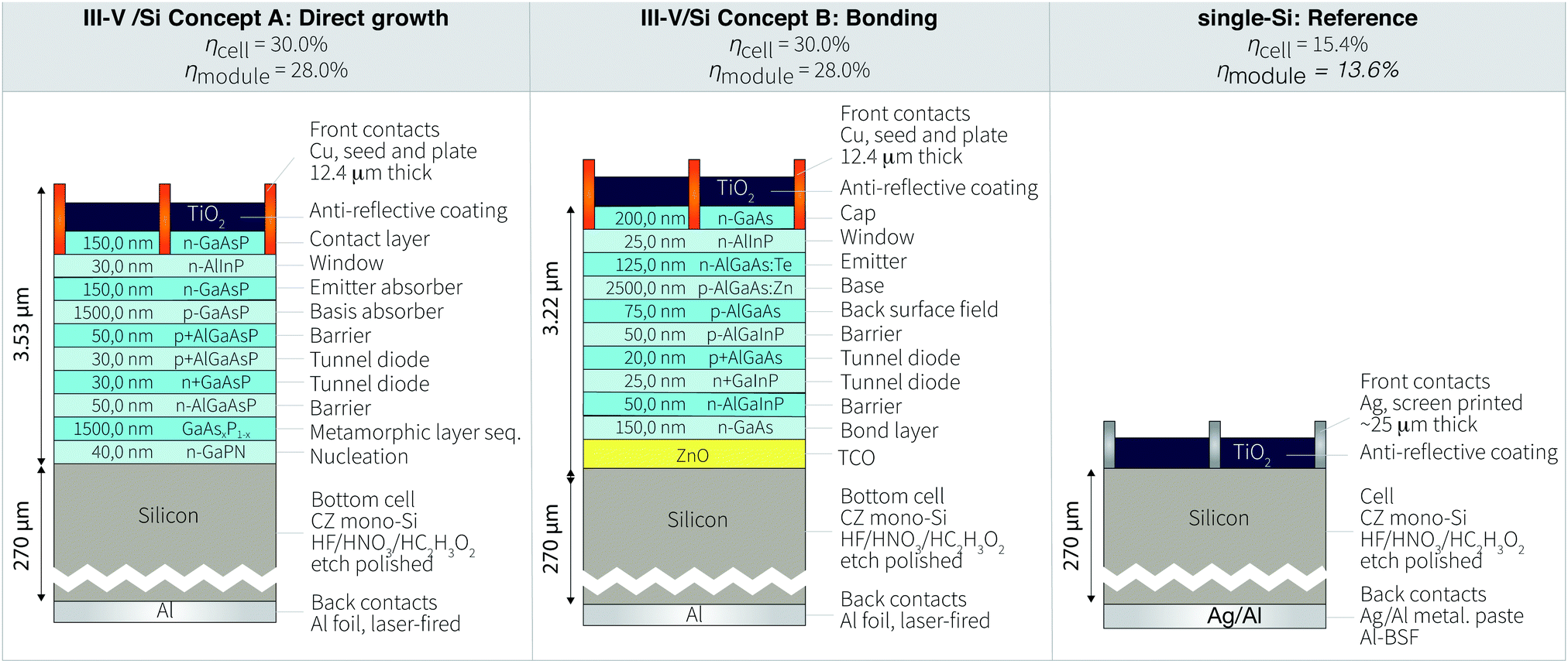 | ||
| Fig. 1 Different types of cells assessed in this study. III–V/Si concepts A and B (left and centre) are being developed by a team led by Fraunhofer ISE. The reference single-Si cell (right) has been modelled as in ecoinvent v3.4. ηcell = cell conversion efficiency; ηmodule = module conversion efficiency. | ||
The manufacturing of III–V/Si cells starts with the silicon wafer that constitutes the bottom cell. This wafer is similar to the one used in commercially available single-Si PV and its manufacturing process is well documented in the ecoinvent database.21 The silicon wafer is then grinded and etched to prepare it for coupling with the additional III–V cells.22 After grinding and etching, the cell is implanted with phosphorus and boron ions which are generated by creating an arc discharge in phosphine and boron trifluoride gas. The ions are then accelerated with specific energies to achieve the desired doping characteristics (e.g. depth of ion concentration and quantity).
This process is followed by annealing, a thermal treatment that helps to activate the dopants and repair any damage caused by the ion implantation process. A passivation layer, which reflects non-absorbed light back into the cell, is added to the backside of the cell by atomic layer deposition (ALD) of a 10 nm film of aluminium oxide (Al2O3). This is followed by plasma enhanced chemical vapour deposition (PECVD) of a silicon nitrate (SiNx) film of 70–100 nm.
The crystalline III–V layers are grown by metalorganic vapour phase epitaxy (MOVPE).23 In MOVPE, hydride gases like arsine (AsH3) and phosphine (PH3), and metalorganic precursors like trimethylgallium (TMGa), trimethylaluminum (TMAl) and trimethylindium (TMIn) flow in a carefully controlled manner into a high temperature (>1000 °C) reactor chamber. The gas flow is supported by an unreactive carrier gas current, typically hydrogen, nitrogen or a combination of both. The molecules for the growth are decomposed in the hot reactor and the III–V layers are formed by deposition of the metal atoms on a crystalline substrate. Two methods to couple the III–V layers with silicon were modelled: direct MOVPE growth of III–V layers on silicon24 (concept A), and MOVPE growth of III–V cells on a gallium arsenide (GaAs) substrate, followed by epitaxial lift-off of the III–V layers and bonding to silicon using a transparent conductive oxide13 (concept B). The GaAs substrate is then reused for growth of new III–V cells.
During MOVPE, some of the process gases deposit as solid waste on the reactor walls, while the toxic exhaust gases are adsorbed in a dry scrubber. We considered a modern dry-scrubbing system, which is passive (no energy required for operation) and uses a copper-based adsorber granulate. Nitrogen and hydrogen gas pass the scrubber unchanged and are vented into the atmosphere. A similar scrubbing process is also implemented for the ion implantation step. Metal contacts are placed on the front of the cell printed using a “seed and plate” technique, where initial patterns for six 75 mm-long fingers are inkjet-printed using a copper-based metallic nanoink. After printing, the printed patterns are sintered using a YAG laser. Conventional electroplating methods are then used to grow the original pattern to a final finger thickness of 12.4 μm and 2 mm width. An antireflective coating is applied on the front side of the cell to minimize reflective losses. A metallic back contact placed using conventional screen-printing methods completes the cell's circuitry.
For the use phase, we considered a system lifetime of 30 years with no degradation, in line with most LCA studies of conventional silicon PV systems. While stability has been a sensitive aspect in LCA studies of some emerging PV technologies such as organic and perovskites,25 III–V multi-junction solar cells are well known for applications in space where reliability is a key concern and significant tests are performed before a product is qualified for a space mission.26 III–V multi-junction cells are also significantly less sensitive to impurities since the absorber thickness is only on the order of 1–3 μm compared to 100–200 μm for Si. This also relaxes the required diffusion length for photogenerated carriers, an important quantity in any solar cell material. Furthermore, the crystals are formed at high temperatures above 600 °C and found to be very stable at operating temperatures up to 120 °C and even above. III–V multi-junction cells have already been deployed in concentrator photovoltaic modules where they operate at around 80 °C with irradiance levels up to 1000 suns. All these harsh conditions have not been leading to any significant signs of degradation, making this technology very suitable for next generation photovoltaics with high reliability.27–29
We excluded electricity distribution, final disposal/recycling and other end-of-life (EOL) options for the III–V/Si cells. We only focused on cradle to gate because the distribution of electricity is not specific to the III–V/Si system, and it is still too early to understand potential recycling options that may be applicable to the III–V/Si cells. We separately discuss the potential implications of recycling in Section 3.5.
The process flowcharts for each manufacturing route are presented in Fig. S1 and S2 in the ESI.† The systems are split between the foreground, which includes new processes specific to the III–V/Si technology, and the background, which includes all the raw materials, transport, energy and ancillary services further upstream in the supply chain.
2.2 Data collection
Input and output data for all background system processes was obtained from the ecoinvent v3.4 database.21 For the foreground processes, we collected data directly from technology developers and secondary sources such as scientific literature and technical equipment/safety data sheets. We used average European electricity markets as modelled in ecoinvent for all foreground electricity inputs and average global markets for raw materials. Many of the processes for manufacturing the III–V prototypes are still lab-based, which could result in unrealistically high consumption of energy and materials. To account for this, we used proxies or extrapolated data where possible in order to represent more realistic industrial-scale processes (e.g. use of in-line tools for wet chemical processes instead of single-use baths). We then attached uncertainties to these extrapolations and assumptions as described in Section 2.4. The full life-cycle inventory of inputs, outputs and data sources for each of the foreground processes is presented in the ESI,† along with the corresponding calculations and assumptions.2.3 Impact assessment
The life-cycle impacts were calculated following the methods recommended by the International Reference Life Cycle Data System (ILCD).30 We calculated impacts across all impact categories recommended by ILCD, including climate change, human toxicity, freshwater ecotoxicity, ionising radiation and depletion of mineral resources (see Section 3.1).2.4 Uncertainty analysis
For emerging technologies, it is often the case that data is unavailable due to commercial sensitivities, is not fully representative as it may be based on lab-scale processes, or can only be expressed as ranges as the technology has not been fine-tuned.31Table 1 summarizes the key processes in the foreground with high uncertainty and the parameters used to characterize them. For the background system, we incorporated the uncertainty information supplied by the ecoinvent v3.4 database.32 We performed an uncertainty analysis by running 1000 Monte Carlo simulations for each alternative PV system.33 We used a dependent sampling method, which takes the same random values for parameters in processes that are shared by the alternative systems in each Monte Carlo run.| Parameter | Distribution | Mode | Min | Max | Criteria |
|---|---|---|---|---|---|
| Hazardous gas abatement – mass of granulate consumed per mass of gas inflow | Triangular | 7.65 kg | 2.55 kg | 7.65 kg | Max value obtained from empirical lab results. Min value based on expert opinion (Fraunhofer ISE, personal communication). Mode set as max for worst-case scenario. |
| GaAs substrate manufacturing – process losses during wafer slicing and polishing | Triangular | 70% | 50% | 70% | Based on Lichtensteiger (2015)34 and Eichler (2012).35 Mode set as max for worst-case scenario. |
| GaAs substrate thickness | Triangular | 550 μm | 450 μm | 650 μm | Based on expert opinion (Joanneum, personal communication). |
| Equipment electricity consumption – calculated as power input (kW) × operating time (h) | Triangular | 75% | 60% | 90% | We assume equipment not always operates at full power, which is especially the case for heating. |
| Energy and mass inputs – taken from technical spec sheet | None | Reported value | — | — | We take the value just as reported in the technical specifications sheet. |
| Energy and mass inputs – taken from commercial brochure | Triangular | Reported value | −20% | +20% | We take the value as reported in the brochure, but add uncertainty that can arise from applying the technology in different conditions. |
| Solvent quantities – taken from peer-reviewed scientific literature, patents & third party lab protocols for chemical synthesis | Triangular | −30% of reported value | −45% | Reported value | Much larger efforts are placed on recycling of solvents in industrial scale. |
| Reactant quantities – taken from peer-reviewed scientific literature, patents & third party lab protocols for chemical synthesis | Triangular | Reported value | −10% | +10% | Reactants are needed in stoichiometric quantities. |
This method provides a more realistic comparison and avoids over or underestimation of variance in the LCA model's outputs.36 We then tested the significance of the difference in impact scores between each alternative PV system using the modified null hypothesis test method proposed by Heijungs et al.37 For this we used the calculation tools for significance testing in LCA developed by Mendoza Beltran et al.38
3 Results & discussion
3.1 Environmental profile
Fig. 2 shows the impacts of the III–V/Si PV systems, taking the single-Si PV system as a comparative reference (100%). The III–V/Si systems have lower scores than the single-Si system across all impact categories except for ionizing radiation and mineral resource depletion (concept B only). The high radiation impact, however, is a consequence of choosing the average European electricity market for the foreground processes, where countries like France and Ukraine contribute significant amounts of nuclear energy. It can also be seen that there is only a very slight difference between the direct growth (concept A) and the bonding (concept B) methods used to manufacture the III–V PV system, across all impact categories except mineral resource depletion.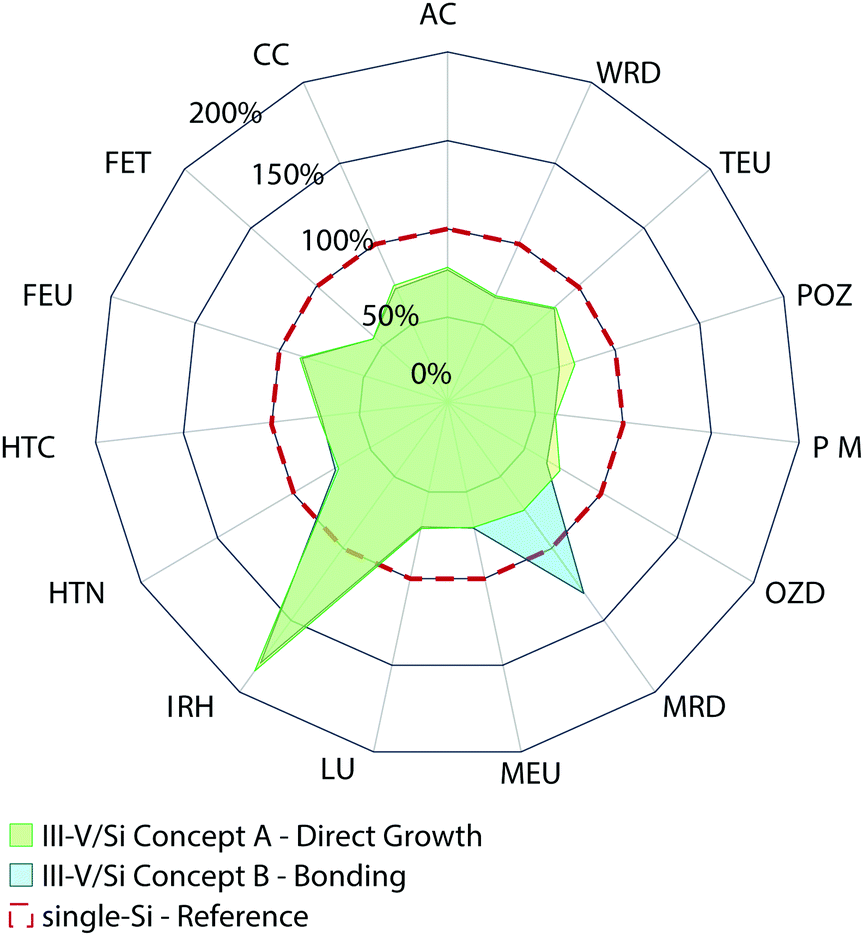 | ||
| Fig. 2 Comparative impact results of III–V/Si PV systems manufactured using both III–V/Si concepts and commercial single-Si (slanted-roof) as modelled in ecoinvent v3.4. AC: acidification; CC: climate change; FET: freshwater ecotoxicity; FEU: freshwater eutrophication; HTC: human toxicity, cancer effects; HTNC: human toxicity, non-cancer effects; IRH: ionising radiation, human health; LU: land use; MEU: marine eutrophication; MRD: mineral, fossil and renewable resource depletion; OD: stratospheric ozone depletion; PM: particulate matter; POZ: photochemical ozone formation; TEU: terrestrial eutrophication; WRD: water resource depletion. | ||
3.2 Key process contributions to impacts
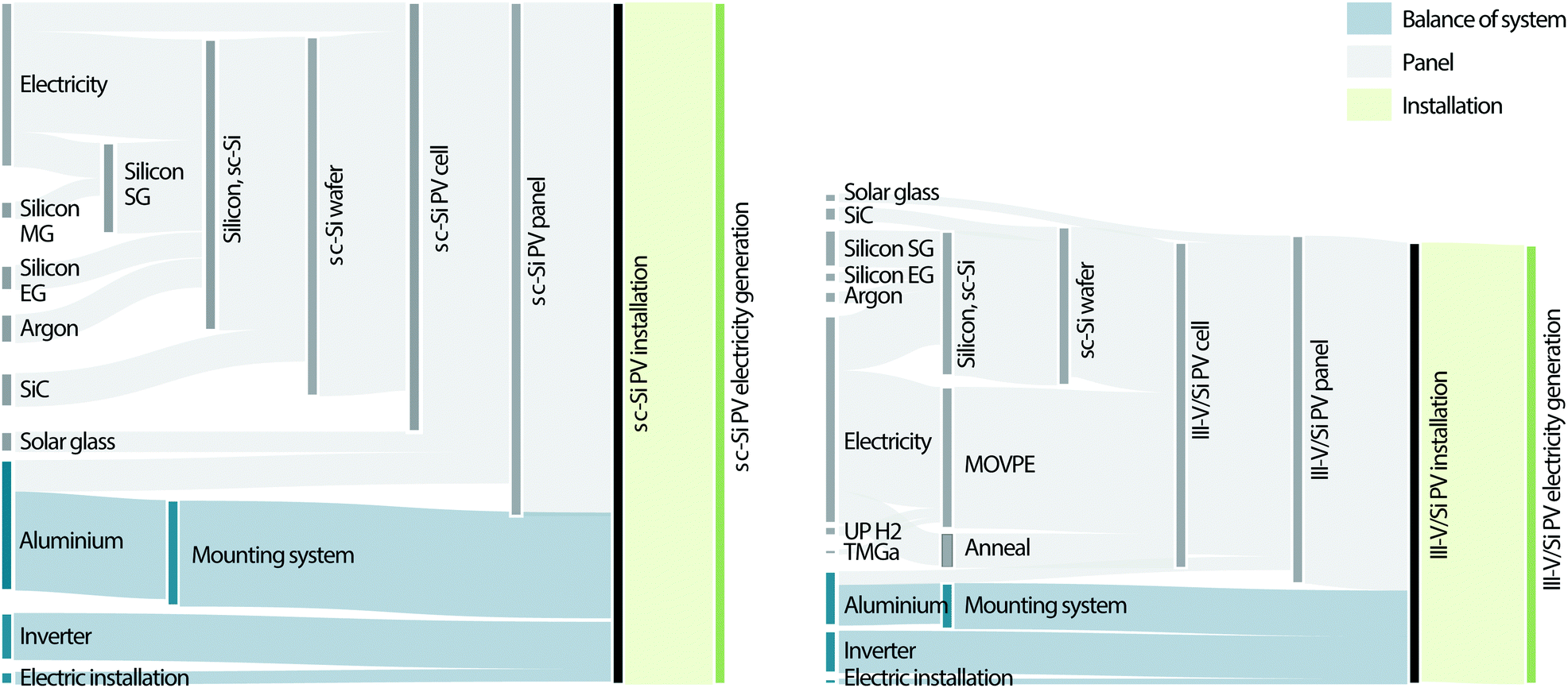 | ||
| Fig. 3 Relative contribution of economic flows and foreground processes to the life cycle climate change impacts of generating electricity with a reference single-Si PV system (left) and a III–V/Si PV system (concept A – direct growth, right). BOS flows are indicated in blue, panel flows in grey. | ||
The manufacturing of the silicon wafer is another dominant process for both III–V/Si and single-Si systems. Here, however, the III–V/Si PV systems draw an advantage from the reduced area required per kWh, which greatly reduces silicon but also panel and balance of system material requirements. The inverter's contribution is not offset by the smaller area because it depends on the power, so its contribution is equal in both III–V/Si and single-Si systems.
Notably, the consumption of ultrapure gases is not an important contribution and, in most cases, falls below the 1% threshold (except for hydrogen and TMGa which contribute 2.06 and 1.15% of the total impact respectively). This is also the case for the front contact metallization. While the manufacturing of engineered nanoparticles does require additional processing energy and materials vs. the bulk silver paste,41,42 the smaller quantity of metal that is used in the nanoink-printed contacts appears to offset the impacts vs. using conventional metallization pastes.
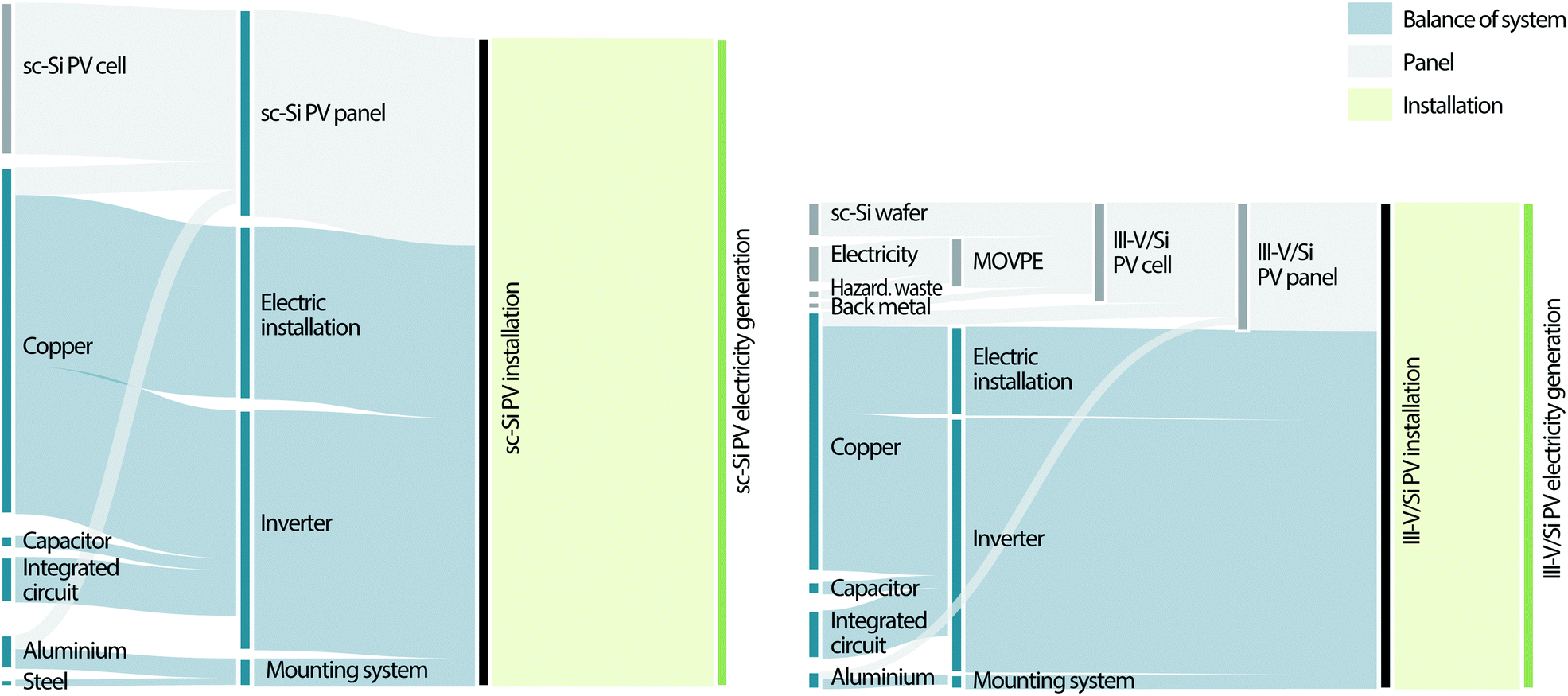 | ||
| Fig. 4 Relative contribution of economic flows and foreground processes to the total life cycle human toxicity (non-cancer effects) impacts of generating electricity with a reference single-Si PV system (left) and a III–V/Si PV system (concept A – direct growth, right). BOS flows are indicated in blue, panel flows in grey. | ||
Notably, the contributions to resource depletion from gallium and indium consumed in the MOVPE process are negligible in comparison. This may be attributable to the low quantities of metalorganic precursors required per cell and the high precursor efficiencies achieved in the Aixtron reactor we modelled (gallium: 38%, indium: 27%, aluminium: 38%). To put these values in perspective, we calculated the consumption of these metals (both identified as critical materials by the European Commission15) for a large-scale yearly production of 1 GWp of III–V/Si cells. Such large-scale manufacturing would consume 818 kg of indium per year. The global refinery production of indium was 760 tonnes in 2019 (estimated).43 Therefore, the III–V/Si market would demand 0.1% of current global supply.
On the other hand, manufacturing 1 GWp of III–V/Si cells would consume approximately 80 tonnes of gallium, ca. 25% of the current world production of primary gallium (320 tonnes in 2019, estimated43). The reason behind the low impact score of gallium in this category is that the ILCD impact assessment method we used is based on a rough estimate of total gallium reserves rather than production.44 According to the U.S. Geological Survey, gallium contained in world resources of bauxite can exceed 1 million tons, and a considerable quantity is also contained in zinc resources.43 Various authors have investigated the criticality of gallium and noted that current supply is still much lower than its actual potential.45,46 As a result, such an increase in demand for III–V/Si cells would not necessarily compromise exploitable reserves, but could significantly change the future supply and market dynamics for gallium.
3.3 Uncertainty analysis
Fig. 5 shows the results of the Monte Carlo simulations and presents the difference in impacts between the conventional single-Si systems and the III–V/Si systems. The positive values indicate a larger impact of single-Si. The Monte Carlo results show that the III–V/Si PV systems are overall likely to perform better environmentally than the commercial single-Si systems modelled in ecoinvent. In most cases, positive results appear to fall well within 75% confidence intervals. The exceptions to this are the impact categories of ionising radiation, where both III–V/Si systems perform worse than single-Si by a factor of between 1 and 2, and resource depletion, where concept A (direct growth) performs worse by a factor of around 0.1–0.5. It can also be seen that concept A performs slightly better than concept B (bonding) in all impact categories, although the difference appears to be relatively small (except for the resource depletion impact category). The modified null hypothesis test with an alpha value of 0.05 further confirmed the statistical significance of these differences. The results of the test are provided in the ESI.†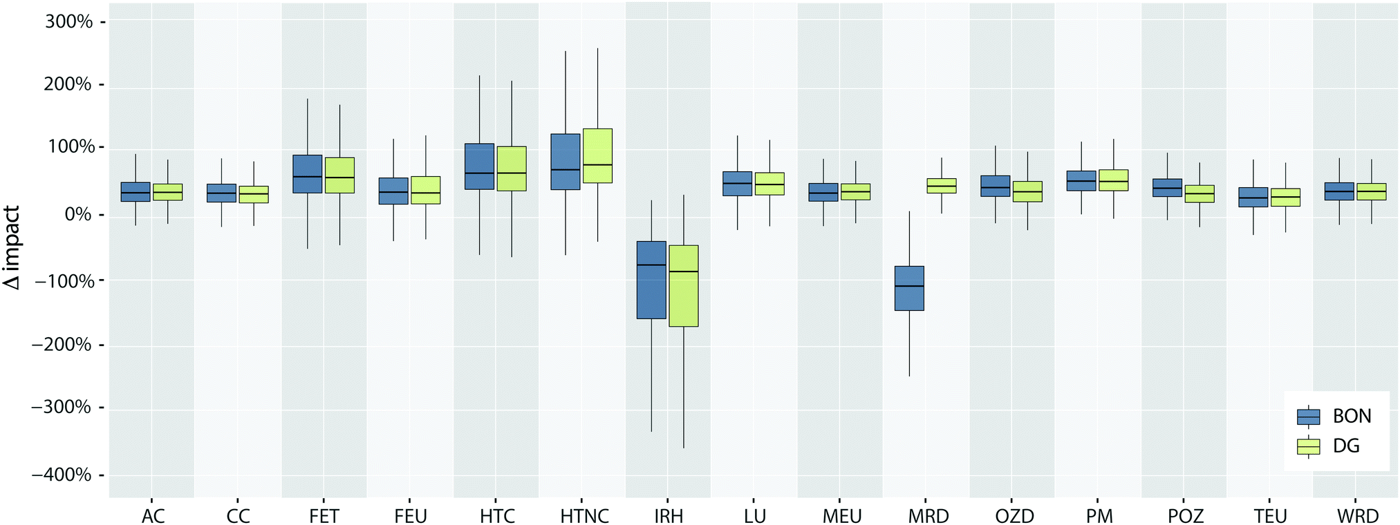 | ||
| Fig. 5 Monte Carlo simulation results for comparative impacts of III–V/Si PV systems vs. the reference single-Si PV system. Values are normalized to the deterministic impact score of the reference single-Si PV system. Positive values indicate a better performance of the III–V/Si systems. The middle line shows the median; the bottom and top edges of the box indicate the 25th and 75th percentiles respectively. The whiskers show minimum and maximum values, with outlier points removed. | ||
3.4 Sensitivity analysis
As shown in Fig. 6, the improved supply chains for silicon and BOS reduce the comparative climate change impact score of the reference single-Si system (Al-BSF) by 34%. These same material reductions lower the climate change impact of the III–V/Si systems by 24% because of the smaller impact of the silicon bottom solar cell and the improved panel and BOS infrastructure. Further implementation of PERC technologies and raising single-Si module conversion efficiencies to 17, 18 and 19% result in additional reductions of 13.3%, 2.7% and 2.3% respectively.
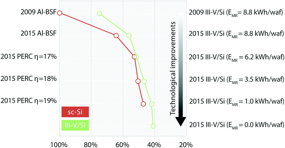 | ||
| Fig. 6 Change in climate change impact scores as a result of technological improvements. 2009: Reference data (2009) for silicon, module and BOS supply chains from ecoinvent v3.4; 2015: Updated IEA PVPS data (2015) for silicon, module and BOS supply chains; η: module efficiency; EMR.: Energy consumption for a single MOVPE run of 31 wafers; waf: calculations based on a 156 × 156 mm2 wafer. | ||
It is also expected that the fabrication of the III–V layers in the III–V/Si tandem cell will improve with the maturity of the technology in the future.49–51 One of the largest contributions to the climate change impact is the energy consumption during the MOVPE process, which currently accounts for 8.8 kWh for one single 156 × 156 mm2 wafer. This consumption was estimated based on a pilot MOVPE reactor design that can process 31 × 4 inch wafers per hour. By comparison, some modern day silicon chemical vapour deposition (CVD) reactors can process over 1000 wafers per hour,52 with energy consumptions as low as 0.014 kW h per wafer. If a similar performance is achieved with the III–V/Si process, this could result in an energy reduction in MOVPE of more than 99%, making the impact contribution of MOVPE almost negligible.
Fig. 6 shows how such expected reductions in MOVPE energy consumption would decrease the comparative climate change impact score of the III–V/Si systems. There is roughly a 5% total impact reduction for each 30% MOVPE energy efficiency improvement. In the best scenario with negligible MOVPE energy consumption, the climate change impact score of the III–V/Si PV system comes down to 38 g CO2eq per kWh electricity generated. In such situation, III–V/Si systems would perform better than the most advanced PERC Si systems in all impact categories except ozone depletion and photochemical ozone formation. In the former category, a small disadvantage (∼3%) remains attributable to the methyl chlorides required for the production of metalorganic compounds. In the latter category, the remaining disadvantage (∼5%) is attributable to the hydrogen gas consumed in the MOVPE process. Similar graphs for other impact categories are provided in the ESI.†
Next to energy efficiency improvements and increased throughput in MOVPE, external policies to increase the participation of renewables in the European energy mix can have an equally important effect. If we take the 2040 projections in the Sustainable Development Scenario proposed by the International Energy Agency,53 with 73% renewables, 16% nuclear, 10% natural gas and 1% coal, the contributions to climate change and human toxicity impacts from MOVPE alone would be reduced by more than 90%.
The sourcing of these carrier and inert gases also merits closer inspection from an environmental perspective. We tested two options for hydrogen; on-site generation with a proton exchange membrane system (PEM) and procuring of commercially available liquefied hydrogen produced off-site via steam methane reforming (SMR). The latter option scored better by a factor of almost 3 in terms of climate change (2.77 vs. 1.04 kg CO2eq per cubic meter of gas) and by a factor of approximately 25 in terms of human health and freshwater ecotoxicity. The poor performance of the PEM system is related to the coal-based fraction of the energy mix. However, this could change significantly if the PEM system is powered with renewable electricity.
In sintering the nanoink-printed front contacts, the laser treatment contributed a negligible amount to all impact categories. We modelled an alternative lab-based process for chemical sintering of the nanoink, using 50 mL of formic acid, 5 mL of ethanol and 42 L of ultrapure nitrogen to sinter a 1 cm2 sample. This process would contribute an additional 0.2 kg CO2eq to climate change, multiplying the total impact of the III–V/Si systems by a factor of nearly 3. An industrial setup for such process would have to be able to sinter a cell area 60 times larger using the same quantities of chemicals in order to keep the impact contribution within 5%. This suggests that laser sintering is a clearly preferred method from an environmental perspective.
3.5 Potential recycling of III–V materials
The environmental benefits and technical feasibility of recycling important quantities of materials like glass, aluminium and silver from conventional silicon PV modules have been discussed by various authors.57 However, even after many years there are still important economic barriers hindering this and today only approximately 10% of silicon PV panels are recycled.58 III–V/Si cells could present additional technical and economic challenges because of the complexity of the crystalline layers. Yet it may still be the case that waste management regulations or constricting markets promote the case for recycling of critical elements like gallium and indium from III–V/Si cells.Scant work has been conducted to date on recycling of III–V cells, but significant work has been published on recycling of light-emitting diodes (LEDs) which have similar compositions of III–V materials and are also grown via MOVPE.59–64 These methods, which include combinations of mechanical, chemical and thermal processing, have been able to recover more than 90% of gallium and indium. Yet they tend to be quite energy intensive, in some cases requiring processing temperatures of up to 1000 °C to be sustained for long periods of time. A detailed assessment of such options is out of scope for this work, but some preliminary calculations can help to set expectations. Each modelled III–V/Si cell contains approximately 2.3 mg of indium and 220 mg of gallium (for concept A). Sourcing these quantities from virgin product adds a CO2 footprint of 0.7 and 54 g CO2eq respectively. These amounts set an upper threshold for the carbon emissions of the proposed recycling processes if environmental benefits are to be derived. For a comparative reference, annealing 100 cells at similarly high temperatures for 1 hour added 40 g CO2eq per cell. Therefore, beyond criticality considerations discussed in Section 3.2.4, it seems challenging for the recovery of III–V materials to deliver significant environmental benefits.
An additional incentive for recovery/recycling of III–V materials from the cells could be the avoidance of possible leaching of toxic arsenic compounds to soil and groundwater. Following a similar calculation as before, each III–V/Si cell contains 360 mg of arsenic. In a pessimistic scenario where the entirety of arsenic leached and infiltrated into groundwater, this would raise the freshwater ecotoxicity impact of the III–V/Si systems by roughly 260%. Note however that this is highly unlikely since the arsenic would be contained in a III–V crystal lattice, and would be much less soluble under normal atmospheric conditions.
4. Conclusions
We can conclude that the environmental outlook of III–V/Si PV systems looks promising if module conversion efficiencies of 28% or above can be reached with a cost competitive product. Our results demonstrate that the higher conversion efficiency of III–V/Si tandem cells can indeed compensate for the impacts of the additional processes and materials used in its manufacturing. Since the operation phase of the III–V/Si system has negligible environmental inputs and outputs, the impacts are almost entirely (>99.99%) embedded in the infrastructure. The infrastructure increases proportionally to the total module area required for the generation of 1 kWh, and the cell area is inversely proportional to cell efficiency. This creates a strong negative correlation between cell conversion efficiency and environmental impact, which reduces not only the impacts of the III–V/Si cell but also of the smaller panel framework and mounting system needed to produce the same amount of electricity.We further showed through a sensitivity analysis that, factoring in technological advances of the past decade for single-PV and further process optimizations during upscaling of III–V/Si, the difference between both systems may eventually become narrower. In such a scenario, the deciding factors may then turn to limitations like space availability in urban areas (favouring III–V/Si) or criticality of specific materials like gallium (favouring single-Si).
Having probed every processing step and their commercially and technically viable alternatives, our investigation produced several important takeaways for III–V technology developers to prioritize in their designs. First, energy efficiency measures in the MOVPE process are the most effective way to improve the environmental profile of III–V PV technologies. Additional room for noticeable improvement in CO2 footprint is in the thermal processing, where rapid thermal annealing or other more energy efficient methods can be pursued. Second, with respect to hazardous gases like arsine and phosphine, we have found that the toxic impacts (from an LCA perspective) are mostly attributed to the use of (primary) copper in the scrubber granulate that is required to absorb the gases. This is due to the fact that, under standard operating conditions, negligible quantities of arsine and phosphine are emitted directly to the environment. Mining copper for the granulate does result in direct environmental emissions of heavy metals and other pollutants. Therefore, the industry's increasing focus on reusing copper in adsorbent granulates is well placed in order to manage the use of these gases sustainably. Third, on-site generation of carrier gases is only preferable when the electricity source powering the systems is mostly renewable. Fourth, epitaxial lift-off and bonding is also an environmentally acceptable manufacturing route insofar as GaAs substrate can be reused at least dozens of times, and the indium trichloride consumption for spray pyrolysis can be reduced or alternative adhesives proposed. In the bonding route, chemical lift-off is preferred over laser lift-off. Finally, chemical sintering of copper ink can introduce significant environmental burdens from the formic acid, therefore a laser sintering method is preferable.
While keeping these elements in mind, it is still the case that larger and more easily achievable improvements for both III–V and single-Si PV systems may come from improving the life-cycle impacts of silicon wafers, panel frame and BOS components, where a large fraction of most impacts resides. These can come from reducing the silicon wafer thickness and losses, and from using recycled or substitute materials for panel (aluminium) and electric components (copper).
Conflicts of interest
There are no conflicts to declare.Acknowledgements
The authors would like to thank Dietmar Schmitz (Aixtron DE), Leif Jensen (TopSil), Jan Benick, Ulrike Heitmann and Jana Wulf (Fraunhofer ISE), Mirella El Gemayel, Roman Trattnig and Nastaran Hayatiroodbari (Joanneum Research), Thomas Bergunde (AZUR Space), Johan Spoelstra and Paul Wentink (Air Liquide), and Georgios Pallas (Leiden University) for their insights and contribution to the data required to conduct this study. This work has received funding from the European Union's Horizon 2020 Research and Innovation Programme within the project SiTaSol under grant agreement no. 727497.Notes and references
- T. D. Lee and A. U. Ebong, Renewable Sustainable Energy Rev., 2017, 70, 1286–1297 CrossRef CAS.
- J.-P. Correa-Baena, A. Abate, M. Saliba, W. Tress, T. Jesper Jacobsson, M. Grätzel and A. Hagfeldt, Energy Environ. Sci., 2017, 10, 710–727 RSC.
- B. Kippelen, J.-L. Brédas, A. Kanwal, S. Miller and M. Chhowalla, Energy Environ. Sci., 2009, 2, 251 RSC.
- S. Zhang, X. Yang, Y. Numata and L. Han, Energy Environ. Sci., 2013, 6, 1443–1464 RSC.
- S. Philipps and W. Warmuth, Photovoltaics Report, Freiburg, Germany, 2018 Search PubMed.
- H. Cotal, C. Fetzer, J. Boisvert, G. Kinsey, R. King, P. Hebert, H. Yoon, N. Karam, S. Kurtz and N. H. Karam, Energy Environ. Sci., 2009, 2, 174–192 RSC.
- Z. Zhou and M. Carbajales-Dale, Energy Environ. Sci., 2018, 11, 603–608 RSC.
- R. Arvidsson, A.-M. Tillman, B. A. Sandén, M. Janssen, A. Nordelöf, D. Kushnir and S. Molander, J. Ind. Ecol., 2018, 22, 1286–1294 CrossRef CAS.
- NREL, Best Research-Cell Efficiency Chart|Photovoltaic Research|NREL, https://www.nrel.gov/pv/cell-efficiency.html, accessed 30 August 2019.
- M. A. Green, Y. Hishikawa, E. D. Dunlop, D. H. Levi, J. Hohl-Ebinger, M. Yoshita and A. W. Y. Ho-Baillie, Prog. Photovoltaics Res. Appl., 2019, 27, 3–12 CrossRef.
- F. Dimroth, in Photovoltaic Solar Energy, John Wiley & Sons, Ltd, Chichester, UK, 2017, pp. 371–382 Search PubMed.
- R. Cariou, J. Benick, P. Beutel, N. Razek, C. Flotgen, M. Hermle, D. Lackner, S. W. Glunz, A. W. Bett, M. Wimplinger and F. Dimroth, IEEE J. Photovoltaics, 2017, 7, 367–373 Search PubMed.
- R. Cariou, J. Benick, F. Feldmann, O. Höhn, H. Hauser and P. Beutel, Nat. Energy, 2018, 3, 1–5 CrossRef.
- S. Essig, C. Allebé, T. Remo, J. F. Geisz, M. A. Steiner, K. Horowitz, L. Barraud, J. S. Ward, M. Schnabel, A. Descoeudres, D. L. Young, M. Woodhouse, M. Despeisse, C. Ballif and A. Tamboli, Nat. Energy, 2017, 2, 17144 CrossRef CAS.
- European Commission, Communication from the Commission to the European Parliament, the Council, the Eureopean Economic and Social Committee and the Committe of the Regions on the 2017 list of Critical Raw Materials for the EU, Brussels, 2017.
- T. E. Graedel, E. M. Harper, N. T. Nassar, P. Nuss and B. K. Reck, Proc. Natl. Acad. Sci. U. S. A., 2015, 112, 4257–4262 CrossRef CAS.
- ISO14040, Int. Organ. Stand., 2006.
- J. B. Guinée, R. Heijungs, G. Huppes, R. Kleijn, A. de Koning, L. van Oers, A. Wegener Sleeswijk, S. Suh, H. A. Udo de Haes, H. de Bruijn, R. van Duin, M. A. J. Huijbregts and M. Gorrée, Life Cycle Assessment: An Operational Guide to the ISO Standards, 2001.
- M. Feifel, J. Ohlmann, J. Benick, M. Hermle, J. Belz, A. Beyer, K. Volz, T. Hannappel, A. W. Bett, D. Lackner and F. Dimroth, IEEE J. Photovoltaics, 2018, 8, 1590–1595 Search PubMed.
- Fraunhofer ISE, 2019.
- G. Wernet, C. Bauer, B. Steubing, J. Reinhard, E. Moreno-Ruiz and B. Weidema, Int. J. Life Cycle Assess., 2016, 21, 1218–1230 CrossRef.
- B. Schwartz and H. Robbins, J. Electrochem. Soc., 1976, 123, 1903 CrossRef CAS.
- M. Feifel, J. Ohlmann, J. Benick, T. Rachow, S. Janz, M. Hermle, F. Dimroth, J. Belz, A. Beyer, K. Volz and D. Lackner, IEEE J. Photovoltaics, 2017, 7, 502–507 Search PubMed.
- M. Feifel, J. Ohlmann, J. Benick, M. Hermle, J. Belz, A. Beyer, K. Volz, T. Hannappel, A. W. Bett, D. Lackner and F. Dimroth, IEEE J. Photovoltaics, 2018, 8, 1590–1595 Search PubMed.
- C. F. Blanco, S. Cucurachi, W. J. G. M. Peijnenburg, A. Beames and M. G. Vijver, Energy Technol., 2020, 1901064 CrossRef.
- American Institute of Aeronautics and Astronautics, Standard: Qualification and Quality Requirements for Space Solar Cells (AIAA S-111A-2014), American Institute of Aeronautics and Astronautics, Inc., 2014.
- T. Gerstmaier, T. Zech, M. Röttger, C. Braun and A. Gombert, in AIP Conference Proceedings, American Institute of Physics Inc., 2015, vol. 1679, p. 030002 Search PubMed.
- M. Muller, D. Jordan and S. Kurtz, in AIP Conference Proceedings, American Institute of Physics Inc., 2015, vol. 1679, p. 020004 Search PubMed.
- C. Algora, in Microelectronics Reliability, Elsevier Ltd, 2010, vol. 50, pp. 1193–1198 Search PubMed.
- European Commission Joint Research Center – Institute for Environmental Sustainability, ILCD Handbook: Recommendations for Life Cycle Impact Assessment in the European context, Luxemburg, 2011.
- S. Gavankar, S. Anderson and A. A. Keller, J. Ind. Ecol., 2015, 19, 468–479 CrossRef CAS.
- B. Weidema, C. Bauer, R. Hischier, C. Mutel, T. Nemecek, C. Vadenbo and G. Wernet, Overview and methodology: data quality guidelines for the ecoinvent database version 3, St. Gallen, Switzerland, 2011 Search PubMed.
- R. Heijungs and M. Lenzen, Int. J. Life Cycle Assess., 2014, 19, 1445–1461 CrossRef.
- L. Lichtensteiger, in 2013 10th China International Forum on Solid State Lighting, ChinaSSL 2013, IEEE, 2015, pp. 85–88.
- S. Eichler, in CS MANTECH Conference, Boston, Massachusetts, USA, 2010 Search PubMed.
- P. J. G. Henriksson, R. Heijungs, H. M. Dao, L. T. Phan, G. R. De Snoo and J. B. Guinée, PLoS One, 2015, 10, 1–11 CrossRef.
- R. Heijungs, P. J. G. Henriksson and J. B. Guinée, Entropy, 2016, 18, 361 CrossRef.
- A. Mendoza Beltran, V. Prado, D. Font Vivanco, P. J. G. Henriksson, J. B. Guinée and R. Heijungs, Environ. Sci. Technol., 2018, 52, 2152–2161 CrossRef CAS.
- K. H. Li, H. S. Alotaibi, H. Sun, R. Lin, W. Guo, C. G. Torres-Castanedo, K. Liu, S. Valdes-Galán and X. Li, J. Cryst. Growth, 2018, 488, 16–22 CrossRef CAS.
- AIXTRON SE, AIX R6 Sets New Standards in LED Manufacturing, https://www.aixtron.com/en/investors/AIXR6 Sets New Standards in LED Manufacturing_n347, accessed 14 December 2019.
- M. Slotte, G. Metha and R. Zevenhoven, Int. J. Energy Environ. Eng., 2015, 6, 233–243 CrossRef CAS.
- L. Pourzahedi and M. J. Eckelman, Environ. Sci.: Nano, 2015, 2, 361–369 RSC.
- U.S. Geological Survey, Mineral Commodity Summaries, Reston, VA, 2020.
- European Commission, Joint Research Centre and Institute for Environment and Sustainability, Characterisation factors of the ILCD Recommended Life Cycle Impact Assessment methods, Database and supporting information., Luxembourg, 2012.
- M. Frenzel, M. P. Ketris, T. Seifert and J. Gutzmer, Resour. Policy, 2016, 47, 38–50 CrossRef.
- M. Frenzel, C. Mikolajczak, M. A. Reuter and J. Gutzmer, Resour. Policy, 2017, 52, 327–335 CrossRef.
- M. M. Lunardi, J. P. Alvarez-Gaitan, N. L. Chang and R. Corkish, Sol. Energy Mater. Sol. Cells, 2018, 187, 154–159 CrossRef.
- R. Frischknecht, R. Itten, P. Sinha, M. de Wild-Scholten, J. Zhang, V. Fthenakis, H. C. Kim, M. Raugei and M. Stucki, Life Cycle Inventories and Life Cycle Assessment of Photovoltaic Systems, 2015.
- D. Brien, M. Dauelsberg, K. Christiansen, J. Hofeldt, M. Deufel and M. Heuken, J. Cryst. Growth, 2007, 303, 330–333 CrossRef CAS.
- M. Dauelsberg, C. Martin, H. Protzmann, A. R. Boyd, E. J. Thrush, J. Käppeler, M. Heuken, R. A. Talalaev, E. V. Yakovlev and A. V. Kondratyev, J. Cryst. Growth, 2007, 298, 418–424 CrossRef CAS.
- A. Beckers, D. Fahle, C. Mauder, T. Kruecken, A. R. Boyd and M. Heuken, SID Symp. Dig. Tech. Pap., 2018, vol. 49, pp. 601–603.
- S. Reber, D. Pocza, M. Keller, M. Arnold, N. Schillinger and D. Krogull, 27th Eur. Photovolt. Sol. Energy Conf. Exhib., 2012, pp. 2466–2470.
- IEA, World Energy Outlook 2019, OECD Publishing, Paris, 2019 Search PubMed.
- X. Wang, Y. Zhang, P. Ning, S. Yan, L. Wang and Q. Ma, RSC Adv., 2017, 7, 56638–56647 RSC.
- O. Schön, B. Schineller, M. Heuken and R. Beccard, J. Cryst. Growth, 1998, 189–190, 335–339 CrossRef.
- A. Meijer, M. A. J. Huijbregts, J. J. Schermer and L. Reijnders, Prog. Photovoltaics Res. Appl., 2003, 11, 275–287 CrossRef CAS.
- R. Deng, N. L. Chang, Z. Ouyang and C. M. Chong, Renewable Sustainable Energy Rev., 2019, 109, 532–550 CrossRef CAS.
- M. M. Lunardi, J. P. Alvarez-Gaitan, J. I. Bilbao and R. Corkish, in Solar Panels and Photovoltaic Materials, ed. B. Zaidi, IntechOpen, 2018 Search PubMed.
- A. Van Den Bossche, W. Vereycken, T. Vander Hoogerstraete, W. Dehaen and K. Binnemans, ACS Sustainable Chem. Eng., 2019, 7, 14451–14459 CrossRef CAS.
- M. Maarefvand, S. Sheibani and F. Rashchi, Hydrometallurgy, 2020, 191, 105230 CrossRef CAS.
- L. Zhan, Y. Zhang, Z. Ahmad and Z. Xu, ACS Sustainable Chem. Eng., 2020, 8, 2874–2882 CrossRef CAS.
- L. Zhan, Z. Wang, Y. Zhang and Z. Xu, Resour., Conserv. Recycl., 2020, 155, 104695 CrossRef.
- L. Zhan, F. Xia, Y. Xia and B. Xie, ACS Sustainable Chem. Eng., 2018, 6, 1336–1342 CrossRef CAS.
- Y. Zhang, L. Zhan, B. Xie, Z. Xu and C. Chen, ACS Sustainable Chem. Eng., 2019, 7, 14111–14118 CrossRef CAS.
Footnote |
| † Electronic supplementary information (ESI) available. See DOI: 10.1039/d0ee01039a |
| This journal is © The Royal Society of Chemistry 2020 |