
 Open Access Article
 This Open Access Article is licensed under a
 Creative Commons Attribution 3.0 Unported Licence
Anisotropic carrier diffusion in single MAPbI3 grains correlates to their twin domains†
Ilka M.
Hermes
 *a,
Andreas
Best
a,
Leonard
Winkelmann
ab,
Julian
Mars
a,
Sarah M.
Vorpahl
c,
Markus
Mezger
ab,
Liam
Collins
d,
Hans-Jürgen
Butt
a,
David S.
Ginger
c,
Kaloian
Koynov
a and
Stefan A. L.
Weber
*ab
*a,
Andreas
Best
a,
Leonard
Winkelmann
ab,
Julian
Mars
a,
Sarah M.
Vorpahl
c,
Markus
Mezger
ab,
Liam
Collins
d,
Hans-Jürgen
Butt
a,
David S.
Ginger
c,
Kaloian
Koynov
a and
Stefan A. L.
Weber
*ab
aMax Planck Institute for Polymer Research, Ackermannweg 10, 55128 Mainz, Germany. E-mail: hermesi@posteo.de
bInstitute of Physics, Johannes Gutenberg University Mainz, Duesbergweg 10-14, 55128 Mainz, Germany. E-mail: webers@mpip-mainz.mpg.de
cDepartment of Chemistry, University of Washington, Seattle, Washington 98105, USA
dCenter for Nanophase Materials Sciences, Oak Ridge National Laboratory, 1 Bethel Valley Rd., Oak Ridge, Tennessee 37830, USA
First published on 2nd June 2020
Abstract
Polycrystalline thin films and single crystals of hybrid perovskites – a material group successfully used for photovoltaic and optoelectronic applications – reportedly display heterogeneous charge carrier dynamics often attributed to grain boundaries or crystalline strain. Here, we locally resolved the carrier diffusion in large, isolated methylammonium lead iodide (MAPbI3) grains via spatial- and time-resolved photoluminescence microscopy. We found that the anisotropic carrier dynamics directly correlate with the arrangement of ferroelastic twin domains. Comparing diffusion constants parallel and perpendicular to the domains showed carriers diffuse around 50–60% faster along the parallel direction. Extensive piezoresponse force microscopy experiments on the nature of the domain pattern suggest that the diffusion anisotropy most likely originates from structural and electrical anomalies at ferroelastic domain walls. We believe that the domain walls act as shallow energetic barriers, which delay the transversal diffusion of carriers. Furthermore, we demonstrate a rearrangement of the domains via heat treatment above the cubic-tetragnal phase transition. Together with the previously reported strain engineering via external stress, our findings promise additional routes to tailor the directionality of the charge carrier diffusion in MAPbI3-based photovoltaics and optoelectronics as well as other ferroelastic materials for optoelectronic applications.
Broader contextMany perovskite compounds exhibit ferroic properties, such as ferromagnetism or ferroelectricity. Among these properties, the lesser known ferro-elasticity originates from a change of the crystal structure below a critical temperature, which introduces an internal strain in the material. To compensate for the internal strain, the crystal forms domains with alternating crystal orientation, often arranged as periodic needle twins that display 90° direction changes. With the integration of the room-temperature ferroelastic perovskite MAPbI3 in photovoltaic and optoelectronic devices, knowing if and how ferroelastic domains affect the electronic charge carrier transport is crucial for device optimization. In this study, we were able to directly correlate an anisotropic charge carrier diffusion with the orientation of ferroelastic twin domains in isolated MAPbI3 grains. Due to the ferroelastic nature of the domains it is possible to modify the domain orientation via external stress and controlled heat treatments above the ferroelastic cubic-tetragonal phase transition of the material. The influence of ferroelastic domains on carrier dynamics offers unique opportunities to customize the directionality of charge carrier transport in the MAPbI3 and other ferroelastic materials studied for optoelectronic applications. |
Introduction
Organic–inorganic hybrid perovskites display astonishing optoelectronic properties making them suitable materials for the active layer in photovoltaics (PV),1–4 light-emitting diodes5 and detectors.6 Among others, a direct band gap,7,8 high defect tolerance9 and long charge carrier diffusion lengths10–12 qualify hybrid perovskites for planar heterojunction devices. As such, the diffusion length in methylammonium lead iodide (MAPbI3) can exceed the usual film thickness of 300–500 nm in perovskite PV devices by up to an order of magnitude.10–12 The diffusion length LD is the average distance photoexcited carriers diffuse before recombining. LD depends on the diffusion constant D via , with the charge carrier lifetime τ.13 While the carrier lifetimes, given by the recombination rates, depend on the trap and carrier density, the diffusion constant is a material property.
However, values reported for the diffusion constant in MAPbI3 vary strongly with significant differences between single crystals and polycrystalline thin films, and even grain-to-grain variations within the same films.14–21 Furthermore, several investigations of charge carrier dynamics in polycrystalline thin films found an anisotropy in the diffusion correlated to limited carrier transport across grain boundaries. The limited inter-grain carrier transport could stem from poor inter-grain connectivity or a mismatch in crystalline orientation.14,22–25 In their study on grain boundary restrictions of the carrier diffusion, Ciesielski et al. resolved an apparent asymmetric spatial distribution of diffusion constants within one single grain.26 This observation raises two questions: do individual MAPbI3 grains display an anisotropic charge carrier diffusion? If so, which mechanism introduces this diffusion anisotropy?
Indeed, Stavrakas et al. recently visualized anisotropic carrier diffusion in MAPbBr3 single crystals. They proposed buried crystal boundaries in the bulk material lead to the diffusion anisotropy.21 Evidence for buried boundaries was delivered by Jariwala et al., who imaged sub-grain boundaries in single MAPbI3 grains via electron backscatter diffraction. These sub-grain boundaries could originate from crystal strain introduced via the cubic-tetragonal phase transition.22
To investigate the diffusion anisotropy in MAPbI3 and the underlying mechanism, we employed spatial- and time-resolved photoluminescence (PL) microscopy23,26–28 as well as piezoresponse force microscopy (PFM). PL microscopy detects photons released during the bimolecular recombination of photoexcited charge carriers. In a sample layout without charge extraction, we could use PL microscopy to map the spatial distribution of diffusive charges upon local excitation. By applying a pulsed excitation, we furthermore detected time-resolved PL decays, which provide information on the carrier dynamics. To probe the carrier diffusion times we scanned the detection of the time-resolved PL over isolated MAPbI3 grains at varying distances from the excitation position. The time-resolved PL decays featured a delayed, distance-dependent diffusion signal, which revealed a distinct diffusion anisotropy. We found that this diffusion anisotropy directly correlated to the arrangement of ferroelastic twin domains, visualized by PFM on the same grains.
Results
Spatial- and time-resolved photoluminescence microscopy
To resolve the lateral distribution of carrier diffusion times in single MAPbI3 grains, we used spatial- and time-resolved PL microscopy: we measured time-resolved PL decays following picosecond excitation pulses in varying distances from the excitation, by moving the detection volume independently from the fixed excitation position over the grain (ESI,† Fig. S1). Previous studies employed similar experimental setups to determine local diffusion constants or evaluate the diffusion across grain boundaries in hybrid perovskites thin films.23,26–28 Here, we focused on investigating diffusion properties of large, isolated MAPbI3 grains; first, to achieve an adequate range of distances between excitation and detection position without resolution limitations, and second, to exclude quenching effects from inter-grain carrier diffusion.The investigated MAPbI3 grain (Fig. 1a) featured 4 arms. At its widest, the grain had a diameter of more than 20 μm, with an overall area of ∼230 μm2. According to Johnston et al. the diffusion length expected for our initial charge carrier density of 1016 cm−3 (see ESI,† calculation S3), is in the order of 10–20 μm10 and, thus, comparable to the dimensions of the grain.
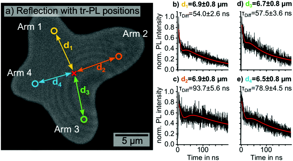 | ||
| Fig. 1 (a) Optical reflection image of the investigated isolated MAPbI3 grain. The detection positions of four exemplary time-resolved PL decays along different grain directions in comparable distances d1, d2, d3 and d4 (6.5–6.9 μm) from the excitation position (red cross) are marked by the yellow, orange, green and blue circle, respectively. (b–e) The four corresponding PL decays detected in distances d1, d2, d3 and d4. The red lines in (b–e) represent the data fits according to eqn (1). Excitation with 633 nm wavelength, a fluence of 0.77 μJ cm−2, a repetition rate of 2 MHz and 0.81 μm beam diameter (ESI,† Fig. S2). | ||
We positioned the pulsed laser excitation in the center of the grain and proceeded to move the detection volume of the time-resolved PL away from the excitation in different directions along the arms. Four exemplary PL decays detected at comparable distances d1, d2, d3 and d4 between 6.5 ± 0.8 and 6.9 ± 0.8 μm from the excitation are shown in Fig. 1b–e.
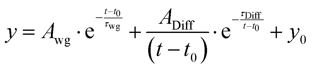
The detected PL decays were of superposition of two signals. In agreement with previous studies,23,26–28 we assigned the fast, initial peak and its associated exponential decay to wave-guided PL emission from the position of the excitation spot. Due to the large mismatch of the refractive indices of air, MAPbI3 and glass, the emission from the excitation position can be trapped in the grain.29–32 The second signal, a delayed peak function, represents PL emitted at the position of the detection volume via bimolecular recombination of diffusive, non-excitonic charge carriers.23,26–28 For quantitative analysis we fitted all time-resolved PL decays with an overlay of an exponential decay and a peak function, given by:
 | (1) |
Comparing the diffusion times τDiff obtained from the data-fits for the four detection positions in Fig. 1b–e, we observed a considerable shift to longer diffusion times for arms 2 (93.7 ± 5.6 ns) and 4 (78.9 ± 4.5 ns), compared to 1 (54.0 ± 2.6 ns) and 3 (57.5 ± 3.6 ns; more PL traces in ESI,† Fig. S4). Previous reports attributed such anisotropic charge carrier diffusion in hybrid perovskites to crystallographic anomalies such as grain boundaries.20–22,33 Multiple groups observed a sharp drop of the static PL distribution at the position of visible as well as buried grain boundaries, which can inhibit the charge carrier transport.14,22,26,33
Static PL distribution
To investigate whether the anisotropy of the diffusion times was caused by buried grain boundaries, we mapped the static PL distribution upon local excitation at the same position as in Fig. 1. The PL distribution was largely homogeneous without sharp intensity drop, which would have indicated the presence of buried grain boundaries (Fig. 2a). Instead, the PL distribution displayed a diffuse maximum in the PL emission at the position of the excitation spot and local maxima at the positions of the grain boundaries, which originated from the enhanced out-coupling of wave-guided PL (Fig. 2a–c).23 Analyzing the line-profiles of PL distribution along the green and black profiles in (a), we observed an anisotropic distribution with an elongated intensity-tail in arm 2. While the PL intensity in arms 1, 3 and 4 dropped by 50% in distances of 3.5, 3.0 and 3.7 μm from the excitation, respectively, in arm 2 the 50%-mark was reached at a distance of 5.7 μm. In light of the long diffusion times observed in arm 2 in the time-resolved PL data, the result from the static PL is surprising. It seems that longer diffusion times correspond neither to a decrease of the carrier density along the same grain direction nor to an increase of non-radiative recombination. We suggest two possible explanations for the time-resolved and static PL microscopy results: either an acceleration of the diffusion along arms 1 and 3 or a deceleration of the diffusion along arms 2 and 4.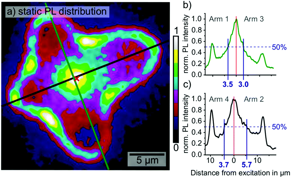 | ||
| Fig. 2 (a) Static PL distribution of the MAPbI3 grain. The position of the excitation laser spot is marked with the red cross. An increased PL is detected at the grain boundaries, most likely due to enhanced outcoupling of wave-guided PL. (b) and (c) show the intensity distributions corresponding to the green and black line-profiles in (a), with local maxima at the position of the excitation as well as the grain boundaries. | ||
For the first scenario, several computational studies proposed a mechanism that would lower the bimolecular recombination and lead to an accelerated diffusion: these calculations showed that charged ferroelectric domain walls as well as polarized ferroelastic domain walls could act as charge-selective carrier pathways, which allow for charge carrier transport with minimized scattering.34–39 The perovskite PV community largely accepted the existence of ferroelasticity in MAPbI3 based on the observation of ferroelastic twin domains with a variety of imaging techniques, including PFM, transmission electron microscopy and polarized light optical microscopy.40–45 Unambiguous evidence for the material's ferroelectricity however remains elusive.43,46,47 In one of the following sections, we investigate ferroelectricity in MAPbI3 by means of advanced PFM measurements.
In the second possible scenario, the grain could have a higher concentration of shallow traps along arm 2 and, to lower extend, along arm 4, which delay the carrier diffusion without acting as non-radiative recombination centers.48,49 The anisotropy in the trap distribution may again relate to ferroelasticity in MAPbI3, with structural and electronic anomalies at the position of domain walls delaying the transversal motion of charge carriers.
Piezoresponse force microscopy
Ferroelectric and -elastic domain patterns can be resolved by PFM — a contact mode scanning probe microscopy method, which applies an AC voltage between a conductive tip and the sample. Since ferroelectric materials are piezoelectric, the AC voltage drives an oscillating piezoresponse. In PFM, the amplitude and phase response of the sample-cantilever system is detected by a lock-in amplifier and recorded while scanning the tip across the surface. Thereby, PFM maps ferroelectric domain patterns.50–52 PFM can image both out-of-plane and in-plane piezoresponses by detecting the vertical or torsional cantilever displacements, respectively.We collected lateral PFM data on the same isolated MAPbI3 grain (Fig. 3). The height signal and the deflection signal showed a grain thickness of 1.1 μm with an overall smooth surface and some terrace-like step edges (Fig. 3a and b, ESI,† Fig. S5). Defined step edges and the flat surface suggested a high crystallinity as well as preferential crystal orientation, confirmed by 2D XRD (ESI,† Fig. S6). In agreement with our previous study, 2D XRD revealed that the majority of the grains on our sample had a (110) orientation parallel to the surface.40 Simultaneously to the height signal, we measured the lateral PFM phase signal (Fig. 3c). In this image, we clearly distinguished a periodic domain pattern, that displayed no correlation to the height signal. Some of the domains spanned over almost the entire width of the grain from arm 1 to arm 3. The direction of the stripes changed by 90° for arm 4 and for the last 3 μm of arm 3 as indicated by the dashed lines in Fig. 3c. The PFM phase profile in Fig. 3d extracted along the red line perpendicular to the domains in Fig. 3c shows that the domain widths varied between 0.13 μm and 0.50 μm.
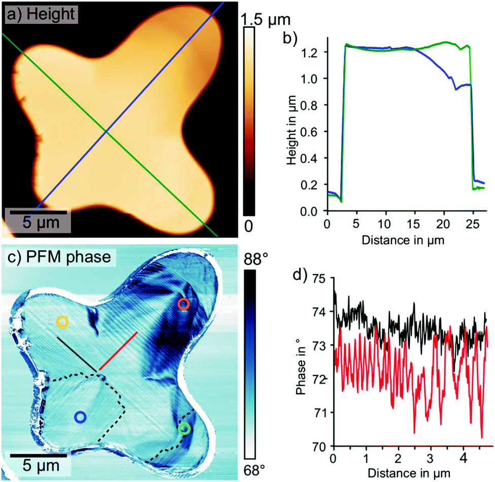 | ||
| Fig. 3 Lateral PFM measurement (1.5 V AC excitation, 735 kHz, 49 nN) on the isolated MAPbI3 grain on glass. (a) Height signal with positions of profiles (green and blue line) shown in (b). (b) Height profiles, extracted at the position of the blue and green line in (a). (c) Lateral PFM phase images periodic twin domains with position of the profiles shown in (d) (solid red and black line). Dashed black lines outline areas with a 90° direction change. The detection positions of the time-resolved PL decays in Fig. 1(b–e) are indicated by the circles. (d) PFM phase line-profiles, extracted at the positions of the solid red and black line in (c), showed the absence of periodicity in the profile parallel to the domains (black) and varying periodicities between 0.13 and 0.50 μm in the profile perpendicular to the domains (red). | ||
When correlating the time-resolved PL decays (Fig. 1b–e) to the periodic domain pattern (Fig. 3c), we observed that shorter diffusion times coincided with a carrier diffusion parallel to the domains, while longer diffusion times coincided with a carrier diffusion perpendicular to the domains. Along arm 1, the carriers exclusively traveled parallel to domains towards the detection position, resulting in the shortest diffusion time (Fig. 1b). Along arm 2, the carriers exclusively diffused perpendicular to the domains, which led to the longest detected diffusion time (Fig. 1c). Along arms 3 and 4 (Fig. 1d and e), the domain orientation changed by 90° between excitation and detection positions. Thus, the diffusion times detected here were combinations of parallel and perpendicular diffusion times. In arm 3, the domain orientation changed from parallel to perpendicular in close proximity to the detection position, giving rise to the shorter diffusion time compared to arm 4.
To evaluate the consistency of the correlation of the diffusion anisotropy and domain arrangement, we compared several PL decays at additional distances parallel and perpendicular to the domains (ESI,† Fig. S7 and S8), inverted the excitation and detection positions (ESI,† Fig. S9) and repeated the PL and PFM measurements on another large, isolated MAPbI3 grain (ESI,† Fig. S10 and S11). In agreement with the initial results, we consistently detected longer diffusion times for diffusion paths perpendicular than for those parallel to the domains. These results suggest that the origin for anisotropic charge carrier diffusion in MAPbI3 perovskite is directly related to the domain pattern resolved via PFM.
Diffusion anisotropy
To quantify the diffusion along both directions of the domain pattern, we plotted the distance d versus the diffusion times τDiff and fitted the diffusion constants D via: | (2) |
For the diffusion parallel to the domains, we obtained a diffusion constant of D‖ = 1.9 ± 0.1 cm2 s−1 and for the perpendicular diffusion a constant of D⊥ = 1.2 ± 0.1 cm2 s−1 (Fig. 4a and b). These values agree with diffusion constants from the literature measured within single grains of polycrystalline MAPbI3 thin films; reported values range between 0.8 and 3.3 cm2 s−1.18,23,26 Calculating the carrier mobilities from the diffusion constants via the Einstein relation, D = μ·kT/q, with the Boltzmann constant k, the temperature T and the charge of the carrier q,13 yields μ‖ = 72 ± 6 cm2 V−1 s−1 in parallel and μ⊥ = 48 ± 4 cm2 V−1 s−1 in perpendicular direction. These mobility values are in the range of mobilities reported for polycrystalline and single crystal MAPbI3.19 Overall, we found that both the diffusion constant as well as the mobility of the charge carriers in the parallel direction were 50–60% higher than perpendicular to the domains, allowing us to quantify the diffusion anisotropy.
 | ||
| Fig. 4 (a) Diffusion times parallel to the domains derived from fits of time-resolved PL decays plotted versus the distance between detection and excitation with the data fit according to eqn (2) and the parallel diffusion constant. (b) Diffusion times perpendicular to the domains derived from fits of time-resolved PL decays plotted versus the distance between detection and excitation with the data fit according to eqn (2) and the perpendicular diffusion constant. | ||
While the fit of the diffusion constants coincided well with the data points at low diffusion times, we observed deviations from the fit for distances of more than 8 μm in both directions. This deviation from the fitted random-walk diffusion model suggests that an additional mechanism affects the carrier diffusion especially at larger distances from the excitation. We exclude a macroscopic drift effect originating from grain boundaries, since diffusion times from the grain center and diffusion times with inverted excitation and detection locations coincide (ESI,† Fig. S9).
A possible candidate for this additional mechanism is photon recycling: a photon emitted via bimolecular recombination can be re-absorbed to create another free carrier pair at some distance from the source. In MAPbI3, the low escape cone and high photoluminescence quantum yield of radiative recombination facilitates photon recycling, since light is kept in the crystal for longer distances, which increases the reabsorption probability.29,30,32,53,54 Photon recycling is a diffusive process, but with higher velocities than pure carrier diffusion.31 Thus, an overlay of pure diffusion and photon recycling would lead to an apparent acceleration of diffusion with increasing distance from the excitation. On the other hand, due to the squared dependence of the radiative recombination on the carrier density, we expect the decrease of the local carrier concentration further from the excitation to result in a lower probability for radiative recombination.10 Therefore, the effect of photon recycling becomes weaker with increasing distances from the excitation (ESI,† Simulation S12).
Mechanistic origin of diffusion anisotropy
The distinct correlation of the diffusion anisotropy and the domain arrangement suggests that the underlying nature of the domains directly affects the carrier transport. By now, several researchers resolved periodic twin domains in MAPbI3 thin films and single crystals, independent of the substrate or the preparation procedure.40–45 A requirement for the observation of the domains is a high crystallinity and, for surface sensitive methods like PFM, a uniform crystal orientation. Previous PFM studies on MAPbI3 delivered contradictory interpretations of the periodic twins.40–43,55–58 While some groups claim the PFM signal originates from ferroelectricity,41,42,55–57 others assigned the PFM signal to competing mechanisms.43,47,58 As such, Liu et al. suggested that the periodic PFM contrast originates from mechanical differences between the domains due to ion redistribution and ferroelasticity instead of ferroelectricity.43,58While the ferroelectric nature of the periodic domains remains under discussion, their ferroelastic nature is widely accepted.40,43–45,58,59 Ferroelastic domains naturally arise from changes of the crystal system to release internal strain.60,61 In MAPbI3, strain is introduced via the cubic-tetragonal phase transition at 54 °C, which occurs during preparation upon cooling to room temperature following the annealing step.7,40,45,62,63 Consequently, periodic ferroelastic twin domains of alternating crystal orientation form.60,61 Ferroelastic domain walls locally disrupt the crystalline order and therefore form energetic barriers. These barriers can act as shallow trap states or scattering centers, which delay the carrier diffusion perpendicular to domains.46 Additionally, Warwick et al. proposed that the structural anomalies in ferroelastic domain walls (∼1 nm in width) in the absence of bulk ferroelectricity introduce a localized in-plane electrical polarization of up to 6 μC cm−2, potentially driving the carrier separation.38 A charge-selective accumulation of electrons or holes in domain walls can introduce an electrostatic repulsion between carriers of the same species within domain walls, thus accelerating the apparent diffusion. This additional local drift effect could explain the observed deviations from the random-walk diffusion in Fig. 4. Likewise, Shi et al. found a suppression of non-radiative recombination in their calculations due to an effective charge carrier separation facilitated by ferroelastic domains, which reduce the electron–phonon coupling.39
On the other hand, theoretical studies on charge separation and transport based on ferroelectricity proposed charged domain walls with 90° head-to-head or tail-to-tail polarization orientation.34–37 However, head-to-head and tail-to-tail orientation states give rise to energetically unstable domain walls due to large depolarization fields and rarely occur naturally.60,64 Instead, a weak charging of head-to-tail domain walls due to slight deviations from the 90° angle induced by internal strain and lattice mismatch is more likely.60,64
To determine the presence or absence of a ferroelectric polarization in MAPbI3 and therefore the decisive driving mechanism behind the diffusion anisotropy, we performed additional PFM experiments on comparable MAPbI3 samples. In particular, we aimed at investigating whether the PFM contrast originates from a true electromechanical (i.e. ferroelectric) response or simply from a contrast in the contact mechanics (i.e. ferroelastic). Changes in tip-sample contact mechanics, e.g. introduced by variations of the contact stiffness, can strongly alter the detected motion of the electrostatically actuated cantilever, even in the absence of piezo- or ferroelectricity.65
First, we investigated the vertical PFM signal with a laser Doppler vibrometer (LDV), as demonstrated previously (Fig. 5a and b).43,65 Here, we observed a strong dependence of the PFM contrast on the laser position of the LDV: when we positioned the laser spot far from the tip on the cantilever, a distinct PFM phase contrast showed a needle shape domain with more than 100° phase difference to the rest of the imaged area (Fig. 5a). However, when the position of the laser coincided with the position of the AFM tip,66 the domain contrast in the PFM phase vanished (Fig. 5b). The dependence of the vertical PFM signal on the laser position suggests that instead of a true electromechanical response, the vertical PFM contrast was caused by changes in the tip-sample contact mechanics or by cantilever buckling. A lateral electromechanical response can introduce a false contrast in the vertical PFM signal due to a buckling motion of the cantilever.40 Overall, we exclude a true out-of-plane electromechanical response as source of the vertical PFM signal.
 | ||
| Fig. 5 Complimentary PFM measurements to investigate the nature of the domain pattern. (a) and (b) show the vertical (vert.) PFM phase measured with a laser Doppler vibrometer (LDV) positioned far away from the tip (a) and on top of the tip (b). (c) lateral (lat.) PFM phase measured via dual amplitude resonance tracking (DART) and the corresponding DART frequency in (d). The cantilever alignment (scan angle 90°) and the scan direction are indicated in the box in the upper right corner. (e) Line profile extracted along the red line in (c). Domain wall positions indicated by the black arrows. (f) Line profile extracted along the red line in d. Domain wall positions indicated by the black arrows. | ||
Since LDV exclusively measures the vertical electromechanical response, we investigated the nature of the lateral PFM signal via dual amplitude resonance tracking (DART) PFM. DART PFM tracks changes in the contact resonance via a feedback system that controls the excitation frequency.67 The DART frequency provides information on the nature of the PFM contrast, since variations in the tip-sample contact stiffness, either due to mechanical or topographic cross-talk, cause changes in the contact resonance.67
By comparing the lateral DART PFM phase and the DART frequency output, we found a coinciding periodic domain pattern in the frequency and in the phase (Fig. 5c–f). For the domains on the left side of the image, where the stripes aligned almost perpendicular to the cantilever, both channels displayed a contrast only at the position of domain walls. In the PFM phase, the domain walls featured an alternating contrast: a domain wall with a lower phase than the bulk followed a domain wall with a larger phase and vice versa. The DART frequency on the other hand, only imaged domain walls with a larger PFM phase as local frequency maxima, while the low phase domain walls were not resolved.
The alternating domain wall contrast in the PFM phase indicates an alternating parallel and antiparallel polarization along the domain walls, as suggested by Warwick et al.38 The reduced domain wall contrast on the vertically aligned domains on the right-hand side of the image supports this hypothesis: here, the cantilever is oriented parallel to the domains and therefore not sensitive to the lateral electromechanical signal along the domain walls. For the bulk domains, on the other hand, we observed a largely uniform PFM phase signal suggesting the absence of a bulk ferroelectricity in MAPbI3.
Meanwhile, the domain wall contrast in the DART frequency originates from local changes in the tip-sample contact mechanics, which shift the contact resonance frequency. Local strain gradients and structural anomalies at ferroelastic domain walls naturally affect the sample's nanomechanical properties and therefore the contact mechanics. As to why only every other domain wall changes the tip-sample contact mechanics, we suggest an impact of the orientation of the local strain gradient, which alternates between adjacent domain walls.38
Based on this in-depth investigation on the origin of the PFM response on MAPbI3, we conclude that the structural and electrical deviations at ferroelastic domain walls from the bulk are the main contribution to the anisotropic carrier diffusion in MAPbI3. In context of the previously proposed mechanisms – an acceleration of the diffusion parallel to the domains or a deceleration of the diffusion perpendicular to the domains – the latter seems to be the governing mechanism. The local disruption of the crystalline order and the strain gradients at the domain walls introduce shallow energy barriers, which delay the transversal motion of charge carriers. However, the apparent presence of a local polarization at the ferroelastic domain walls may lead to an additional acceleration effect of the charge carriers.38 Lastly, we did not observe indications for charged ferroelectric domain walls as previously proposed.34–37
In applied perovskite devices, the effect of the anisotropic carrier diffusion on the vertical carrier transport depends on the texture of the polycrystalline MAPbI3 thin films: Rothmann et al. proposed a 45° angle of the domain walls with respect to the (110) crystal plane.45 For highly oriented thin films, we expect the influence on the diffusion anisotropy to be minor along the 45° domain walls. However, in thin films with random crystal orientations of the constituent grains the impact of the diffusion anisotropy could introduce heterogeneities in the inter-grain carrier diffusion as previously reported.14,22–25
Manipulation of the domain arrangement
The relation between ferroelastic domain pattern and carrier diffusion offers new paths of device improvement for PSCs or perovskite-based optoelectronics by customizing the directionality of the carrier diffusion. Similar to other ferroic properties, the crystal orientation in ferroelastic domains can be switched upon application of an external stress.60 Strelcov et al. demonstrated this stress-induced ferroelastic domain switching already in 2017.44 Here, we focused on the effect of heat treatments on the domain alignment. As such, we found that heating a freshly annealed MAPbI3 sample with a predominantly irregular domain pattern over the ferroelastic cubic-tetragonal phase transition temperature of 54 °C7,62,63 led to a complete disappearance of the domain pattern, further confirming the ferroelastic nature of the domains (Fig. 6a and b). Upon cooling the sample back to room temperature with a well-defined cooling rate of 1 °C per minute, the domain pattern reappeared with a changed arrangement: an increase of the domain density and more regular spacings between the domains (Fig. 6c). We suggest that the abrupt cooling after the annealing step introduced the disorder and the lower domain density in the initial state of the sample, while the well-defined cooling rates resulted in an ordered, high density domain arrangement. | ||
| Fig. 6 AFM topography (top row) and corresponding lateral PFM phase (a) before (at 26 °C), (b) during (at 70 °C) and (c) after (at 27 °C) the heating experiment over the cubic-tetragonal phase transition at 54 °C, visualizing a change in the domain pattern following the heating cycle. | ||
Therefore, targeted heat treatment as well as stress-induced domain switching should be explored as future pathways to either reduce the anisotropy in the carrier diffusion by lowering the domain density or to introduce a preferential directionality in the carrier diffusion, by parallel domain alignment.
Conclusions
Via spatial- and time-resolved PL microscopy we resolved an anisotropic distribution of carrier diffusion times on isolated MAPbI3 grains. This anisotropic charge carrier diffusion directly correlates to the arrangement of ferroelastic twin domains, which form to reduce crystalline strain due to the cubic-tetragonal phase transition. Quantitative analysis of the diffusion dependence on the domain arrangement gave a 50–60% higher diffusion constant parallel (D‖ = 1.9 ± 0.1 cm2 s−1) than perpendicular to the domains (D⊥ = 1.2 ± 0.1 cm2 s−1). Extensive PFM investigations on the underlying nature of the domains indicated the presence of local strain gradients and crystallographic inhomogeneities, as well as an electrical polarization at ferroelastic domain walls. We propose that these structural and electrical anomalies at the domain walls act as energetic barriers, which delay the carrier diffusion perpendicular to the domains, introducing the diffusion anisotropy. Finally, we showed the possibility to manipulate the domain pattern via heat treatment above the phase transition temperature, opening new routes for optimizing optoelectronic devices based on MAPbI3 and other ferroelastic materials.Experimental
Sample preparation
For the preparation of the MAPbI3 thin films, we dissolved the precursors methylammonium iodide CH3NH3I (Methylammonium iodide was synthesized as described by Lee et al.)68 and PbCl2 (Sigma-Aldrich, 99.999%) in a 3![[thin space (1/6-em)]](https://www.rsc.org/images/entities/char_2009.gif) :1 ratio with a concentration of 40 wt% in anhydrous dimethylformamide (Sigma-Aldrich). We cleaned glass coverslips with thickness of 150 μm in an ultrasound bath for 15 minutes each in 2% Hellmanex solution, deionized water, acetone and isopropanol, in this order. The ultrasound cleaning was followed by a 5 minute treatment in oxygen plasma. The spin-coating of the solution onto the coverslips was performed in a nitrogen glovebox at 1750 rpm for 60 s with an acceleration of 250 rpm s−1. Afterwards the samples annealed at room temperature for 30 minutes in the glovebox, followed by a solvent annealing69 step at 100 °C for 60 min in air on a preheated hot plate. Immediately after the solvent annealing, we transferred the samples into another nitrogen glovebox, equipped with an atomic force microscope (AFM).
:1 ratio with a concentration of 40 wt% in anhydrous dimethylformamide (Sigma-Aldrich). We cleaned glass coverslips with thickness of 150 μm in an ultrasound bath for 15 minutes each in 2% Hellmanex solution, deionized water, acetone and isopropanol, in this order. The ultrasound cleaning was followed by a 5 minute treatment in oxygen plasma. The spin-coating of the solution onto the coverslips was performed in a nitrogen glovebox at 1750 rpm for 60 s with an acceleration of 250 rpm s−1. Afterwards the samples annealed at room temperature for 30 minutes in the glovebox, followed by a solvent annealing69 step at 100 °C for 60 min in air on a preheated hot plate. Immediately after the solvent annealing, we transferred the samples into another nitrogen glovebox, equipped with an atomic force microscope (AFM).
Spatial- and time-resolved photoluminescence (PL)
For the excitation, we used a picosecond laser (Hamamatsu Picosecond Light Pulser PLP-10) with a pulse width of 95 ± 5 ps at 635 nm wavelength, repetition rates of 2 MHz (for time-resolved PL) and 20 MHz (for static PL) and fluences between 0.77 and 0.89 μJ cm−2 (ESI,† Fig. S1). Due to the large bandwidth of the excitation laser, the beam was guided through a 633 nm clean-up filter (Semrock, 632.8 nm MaxLine) with a bandwidth of 2.4 nm FWHM, changing the center wavelength to 633 nm. The excitation light was focused via a 20× objective (Olympus LMPLFL20, numerical aperture NA = 0.4) onto the sample surface with a spot diameter of 0.81 μm at FWHM and 1.4 μm 1/e2 width (ESI,† Fig. S2). The sample was placed onto the stage of an inverted microscope (Olympus IX70) equipped with a 50× objective (Olympus MPLAPO50, NA = 0.95) and coupled to a Olympus FluoView FV300 confocal laser scanning unit. For the static PL measurements, the collected PL was detected with a photomultiplier, after passing a dichroic mirror, the pinhole (300 μm) and a 660 nm longpass filter (Chroma HQ660LP). For the time-resolved PL, after passing the pinhole (60 μm), the collected PL emission was guided through an optical fiber to a PicoQuant detection unit equipped with two single photon avalanche diodes (τ-SPAD) connected to a TCSPC board (TimeHarp 200). In front of the diodes, a 635 nm long pass filter (Semrock, 635 nm Edge Basic) and a 633 nm notch filter (Semrock, 633 nm StopLine Single-notch) with a bandwidth of 25 nm were placed, respectively. For a pinhole of 60 μm and the 50× objective, the detection spot had a radius of 0.18 μm for a wavelength of 765 nm. The instrument response function was ∼1.4 ns at FWHM. During the scan, nitrogen was continuously flowing over the sample to avoid degradation (ESI,† Fig. S13).Piezoresponse force microscopy (PFM)
Lateral PFM was measured on an MFP-3D atomic force microscope from Asylum Research (Oxford Instruments) and a Zürich Instruments HF2 lock-in amplifier in a nitrogen glovebox. The measurements were performed at room temperature with conductive platinum–iridium coated SCM PIT-V2 cantilevers from Bruker with free resonance frequencies of 70 kHz and spring constants of k ∼2.5 nN nm−1. We measured the lateral PFM signal at AC excitation voltages with peak amplitudes of 1.5 V close to the lateral contact resonance at 735 kHz to utilize the resonance enhancement. As back electrodes, we used aluminum. To mark the PFM-characterized sample areas for the PL microscopy we scratched a pattern into the MAPbI3 film and measured close to a scratch.The LDV-PFM measurements were performed using a commercial Cypher ES AFM (Asylum Research, Santa Barbara, CA) with an integrated quantitative Laser Doppler Vibrometer (LDV) system (Polytec GmbH, Waldbronn, Germany) to achieve highly sensitive electromechanical imaging and spectroscopy. Measurements were performed using Pt/Ir-coated cantilevers (ElectriMulti 75G from Budget Sensors) with a nominal spring constant of ∼3 N m−1 and resonance frequency of ∼75 kHz. All measurements were captured at room temperature under nitrogen flow. We measured the LDV-PFM signal at AC excitation voltages with peak amplitudes of 2 V at 265 kHz.
For the lateral dual amplitude resonance tracking (DART) experiments, we again used the MFP-3D atomic force microscope from Asylum Research (Oxford Instruments) in a nitrogen glovebox with SCM PIT-V2 cantilevers with free resonance frequencies of 70 kHz and spring constants of k ∼2.5 nN nm−1 at room temperature. The lateral contact resonance was at 746 kHz and the two sidebands for the frequency tracking were generated at 1.5 kHz from the resonance. The AC drive was 1.5 V.
The heating experiment was performed on a Cypher ES AFM (Oxford Instruments) in nitrogen atmosphere. For the lateral PFM measurements, we used a platinum–iridium coated PPP-EFM cantilever with a free resonance frequency of 75 kHz and spring constants of k ∼ 2.8 nN nm−1. The AC drive was 1.5 V at 675 kHz. The sample temperature before the heating step was 26 °C. Afterwards the sample was heated at 1 °C min−1 to 70 °C. We waited around 30 min for the sample temperature to equilibrate before measuring. Afterwards the sample was cooled to 27 °C and we waited around 30 min for the sample temperature to equilibrate before measuring the PFM signal.
X-ray diffraction (XRD)
X-ray diffraction on the MAPbI3 film was measured on a 6-circle diffractometer using Cu Kα radiation (Rigaku MicroMax 007 Xray generator, Osmic Confocal Max-Flux curved multilayer optics). The sample was mounted in reflection geometry at an incident angle of 4.5°. 2D scattering patterns were collected on an image plate detector (Mar345, 150 μm pixel size) at a sample-detector distance of 356.83 mm.Conflicts of interest
There are no conflicts to declare.Acknowledgements
I. M. H. acknowledges ERC Grant No. 340391 SuPro for funding. D. S. G. and S. M. H. acknowledge support from the DOE (DE-SC0013957). LDV-PFM was conducted at the Center for Nanophase Materials Sciences, which is a DOE Office of Science User Facility. PFM during heat treatment was conducted at the Molecular Analysis Facility, a National Nanotechnology Coordinated Infrastructure site at the University of Washington, which is supported in part by the National Science Foundation (Grant ECC-1542101), the University of Washington, the Molecular Engineering & Sciences Institute, the Clean Energy Institute, and the National Institutes of Health. We thank Rüdiger Berger and Denis Andrienko for helpful discussions. Open Access funding provided by the Max Planck Society.References
- A. Kojima, K. Teshima, Y. Shirai and T. Miyasaka, J. Am. Chem. Soc., 2009, 131, 6050–6051 CrossRef CAS PubMed.
- M. M. Lee, J. Teuscher, T. Miyasaka, T. N. Murakami and H. J. Snaith, Science, 2012, 338, 643–647 CrossRef CAS PubMed.
- H.-S. Kim, C.-R. Lee, J.-H. Im, K.-B. Lee, T. Moehl, A. Marchioro, S.-J. Moon, R. Humphry-Baker, J.-H. Yum and J. E. Moser, Sci. Rep., 2012, 2, 591 CrossRef PubMed.
- J. J. Yoo, S. Wieghold, M. C. Sponseller, M. R. Chua, S. N. Bertram, N. T. P. Hartono, J. S. Tresback, E. C. Hansen, J.-P. Correa-Baena and V. Bulović, Energy Environ. Sci., 2019, 12, 2192–2199 RSC.
- O. A. Jaramillo-Quintero, R. S. Sanchez, M. Rincon and I. Mora-Sero, J. Phys. Chem. Lett., 2015, 6, 1883–1890 CrossRef CAS PubMed.
- A. Z. Ashar, N. Ganesh and K. S. Narayan, Adv. Electron. Mater., 2018, 4, 1700362 CrossRef.
- C. C. Stoumpos, C. D. Malliakas and M. G. Kanatzidis, Inorg. Chem., 2013, 52, 9019–9038 CrossRef CAS PubMed.
- T. J. Jacobsson, J.-P. Correa-Baena, M. Pazoki, M. Saliba, K. Schenk, M. Grätzel and A. Hagfeldt, Energy Environ. Sci., 2016, 9, 1706–1724 RSC.
- K. X. Steirer, P. Schulz, G. Teeter, V. Stevanovic, M. Yang, K. Zhu and J. J. Berry, ACS Energy Lett., 2016, 1, 360–366 CrossRef CAS.
- M. B. Johnston and L. M. Herz, Acc. Chem. Res., 2016, 49, 146–154 CrossRef CAS PubMed.
- S. D. Stranks, G. E. Eperon, G. Grancini, C. Menelaou, M. J. P. Alcocer, T. Leijtens, L. M. Herz, A. Petrozza and H. J. Snaith, Science, 2013, 342, 341–344 CrossRef CAS PubMed.
- D. Shi, V. Adinolfi, R. Comin, M. Yuan, E. Alarousu, A. Buin, Y. Chen, S. Hoogland, A. Rothenberger and K. Katsiev, Science, 2015, 347, 519–522 CrossRef CAS PubMed.
- G. Hodes and P. V. Kamat, J. Phys. Chem. Lett., 2015, 6, 4090–4092 CrossRef CAS PubMed.
- D. W. DeQuilettes, S. Jariwala, S. Burke, M. E. Ziffer, J. T.-W. Wang, H. J. Snaith and D. S. Ginger, ACS Nano, 2017, 11, 11488–11496 CrossRef CAS PubMed.
- M. Vrućinić, C. Matthiesen, A. Sadhanala, G. Divitini, S. Cacovich, S. E. Dutton, C. Ducati, M. Atatüre, H. Snaith and R. H. Friend, Adv. Sci., 2015, 2, 1500136 CrossRef PubMed.
- Z. Guo, J. S. Manser, Y. Wan, P. V. Kamat and L. Huang, Nat. Commun., 2015, 6, 7471 CrossRef CAS PubMed.
- Y. Chen, H. T. Yi, X. Wu, R. Haroldson, Y. N. Gartstein, Y. I. Rodionov, K. S. Tikhonov, A. Zakhidov, X.-Y. Zhu and V. Podzorov, Nat. Commun., 2016, 7, 1–9 Search PubMed.
- A. H. Hill, K. E. Smyser, C. L. Kennedy, E. S. Massaro and E. M. Grumstrup, J. Phys. Chem. Lett., 2017, 8, 948–953 CrossRef CAS PubMed.
- L. M. Herz, Ann. Rev. Phys. Chem., 2016, 67, 65–89 CrossRef CAS PubMed.
- G. Delport, S. Macpherson and S. D. Stranks, arXiv Prepr., arXiv1911.10615.
- C. Stavrakas, G. Delport, A. A. Zhumekenov, M. Anaya, R. Chahbazian, O. M. Bakr, E. S. Barnard and S. D. Stranks, ACS Energy Lett., 2019, 5, 117–123 CrossRef PubMed.
- S. Jariwala, H. Sun, G. W. P. Adhyaksa, A. Lof, L. A. Muscarella, B. Ehrler, E. C. Garnett and D. S. Ginger, Joule, 2019, 3, 3048–3060 CrossRef CAS.
- W. Tian, R. Cui, J. Leng, J. Liu, Y. Li, C. Zhao, J. Zhang, W. Deng, T. Lian and S. Jin, Angew. Chem., Int. Ed., 2016, 55, 13067–13071 CrossRef CAS PubMed.
- O. G. Reid, M. Yang, N. Kopidakis, K. Zhu and G. Rumbles, ACS Energy Lett., 2016, 1, 561–565 CrossRef CAS.
- N. Cho, F. Li, B. Turedi, L. Sinatra, S. P. Sarmah, M. R. Parida, M. I. Saidaminov, B. Murali, V. M. Burlakov and A. Goriely, Nat. Commun., 2016, 7, 1–11 Search PubMed.
- R. Ciesielski, F. Schäfer, N. F. Hartmann, N. Giesbrecht, T. Bein, P. Docampo and A. Hartschuh, ACS Appl. Mater. Interfaces, 2018, 10, 7974–7981 CrossRef CAS PubMed.
- W. Tian, C. Zhao, J. Leng, R. Cui and S. Jin, J. Am. Chem. Soc., 2015, 137, 12458–12461 CrossRef CAS PubMed.
- K. Handloser, N. Giesbrecht, T. Bein, P. Docampo, M. Handloser and A. Hartschuh, ACS Photonics, 2016, 3, 255–261 CrossRef CAS.
- Y. Yamada, T. Yamada, L. Q. Phuong, N. Maruyama, H. Nishimura, A. Wakamiya, Y. Murata and Y. Kanemitsu, J. Am. Chem. Soc., 2015, 137, 10456–10459 CrossRef CAS PubMed.
- L. M. Pazos-Outón, M. Szumilo, R. Lamboll, J. M. Richter, M. Crespo-Quesada, M. Abdi-Jalebi, H. J. Beeson, M. Vrućinić, M. Alsari and H. J. Snaith, Science, 2016, 351, 1430–1433 CrossRef PubMed.
- T. W. Crothers, R. L. Milot, J. B. Patel, E. S. Parrott, J. Schlipf, P. Müller-Buschbaum, M. B. Johnston and L. M. Herz, Nano Lett., 2017, 17, 5782–5789 CrossRef CAS PubMed.
- J. M. Richter, M. Abdi-Jalebi, A. Sadhanala, M. Tabachnyk, J. P. H. Rivett, L. M. Pazos-Outón, K. C. Gödel, M. Price, F. Deschler and R. H. Friend, Nat. Commun., 2016, 7, 1–8 Search PubMed.
- W. Li, S. K. Yadavalli, D. Lizarazo-Ferro, M. Chen, Y. Zhou, N. P. Padture and R. Zia, ACS Energy Lett., 2018, 3, 2669–2670 CrossRef CAS.
- J. M. Frost, K. T. Butler, F. Brivio, C. H. Hendon, M. Van Schilfgaarde and A. Walsh, Nano Lett., 2014, 14, 2584–2590 CrossRef CAS PubMed.
- S. Liu, F. Zheng, N. Z. Koocher, H. Takenaka, F. Wang and A. M. Rappe, J. Phys. Chem. Lett., 2015, 6, 693–699 CrossRef CAS PubMed.
- A. Pecchia, D. Gentilini, D. Rossi, M. Auf der Maur and A. Di Carlo, Nano Lett., 2016, 16, 988–992 CrossRef CAS PubMed.
- D. Rossi, A. Pecchia, M. A. der Maur, T. Leonhard, H. Röhm, M. J. Hoffmann, A. Colsmann and A. Di Carlo, Nano Energy, 2018, 48, 20–26 CrossRef CAS.
- A. R. Warwick, J. Íñiguez, P. D. Haynes and N. C. Bristowe, J. Phys. Chem. Lett., 2019, 10, 1416–1421 CrossRef CAS PubMed.
- R. Shi, Z. Zhang, W. Fang and R. Long, Nanoscale Horiz., 2020, 5, 683–690 RSC.
- I. M. Hermes, S. A. Bretschneider, V. W. Bergmann, D. Li, A. Klasen, J. Mars, W. Tremel, F. Laquai, H.-J. Butt, M. Mezger, R. Berger, B. J. Rodriguez and S. A. L. Weber, J. Phys. Chem. C, 2016, 120, 5724–5731 CrossRef CAS.
- S. M. Vorpahl, R. Giridharagopal, G. E. Eperon, I. M. Hermes, S. A. L. Weber and D. S. Ginger, ACS Appl. Energy Mater., 2018, 1, 1534–1539 CrossRef CAS.
- H. Röhm, T. Leonhard, M. J. Hoffmann and A. Colsmann, Energy Environ. Sci., 2017, 10, 950–955 RSC.
- Y. Liu, L. Collins, R. Proksch, S. Kim, B. R. Watson, B. Doughty, T. R. Calhoun, M. Ahmadi, A. V. Ievlev and S. Jesse, Nat. Mater., 2018, 17, 1013–1019 CrossRef CAS PubMed.
- E. Strelcov, Q. Dong, T. Li, J. Chae, Y. Shao, Y. Deng, A. Gruverman, J. Huang and A. Centrone, Sci. Adv. Adv., 2017, 3, e1602165 CrossRef PubMed.
- M. U. Rothmann, W. Li, Y. Zhu, U. Bach, L. Spiccia, J. Etheridge and Y.-B. Cheng, Nat. Commun., 2017, 8, 1–8 CrossRef PubMed.
- M. Coll, A. Gomez, E. Mas-Marza, O. Almora, G. Garcia-Belmonte, M. Campoy-Quiles and J. Bisquert, J. Phys. Chem. Lett., 2015, 6, 1408–1413 CrossRef CAS PubMed.
- A. Gómez, Q. Wang, A. R. Goñi, M. Campoy-Quiles and A. Abate, Energy Environ. Sci., 2019, 12, 2537–2547 RSC.
- A. Castro-Méndez, J. Hidalgo and J. Correa-Baena, Adv. Energy Mater., 2019, 9, 1901489 CrossRef.
- Y. Shao, Z. Xiao, C. Bi, Y. Yuan and J. Huang, Nat. Commun., 2014, 5, 1–7 Search PubMed.
- E. Soergel, J. Phys. D: Appl. Phys., 2011, 44, 464003 CrossRef.
- S. V. Kalinin and A. Gruverman, Scanning probe microscopy: electrical and electromechanical phenomena at the nanoscale, Springer, 2007, vol. 1 Search PubMed.
- A. Gruverman and S. V. Kalinin, J. Mater. Sci., 2006, 41, 107–116 CrossRef CAS.
- T. Kirchartz, F. Staub and U. Rau, ACS Energy Lett., 2016, 1, 731–739 CrossRef CAS.
- M. Ansari-Rad and J. Bisquert, Phys. Rev. Appl., 2018, 10, 34062 CrossRef CAS.
- B. Huang, G. Kong, E. N. Esfahani, S. Chen, Q. Li, J. Yu, N. Xu, Y. Zhang, S. Xie and H. Wen, npj Quantum Mater., 2018, 3, 1–8 CrossRef CAS.
- L. M. Garten, D. T. Moore, S. U. Nanayakkara, S. Dwaraknath, P. Schulz, J. Wands, A. Rockett, B. Newell, K. A. Persson and S. Trolier-McKinstry, Sci. Adv., 2019, 5, eaas9311 CrossRef PubMed.
- T. Leonhard, A. D. Schulz, H. Röhm, S. Wagner, F. J. Altermann, W. Rheinheimer, M. J. Hoffmann and A. Colsmann, Energy Technol., 2019, 7, 1800989 CrossRef.
- Y. Liu, L. Collins, A. Belianinov, S. M. Neumayer, A. V. Ievlev, M. Ahmadi, K. Xiao, S. T. Retterer, S. Jesse and S. V. Kalinin, Appl. Phys. Lett., 2018, 113, 72102 CrossRef.
- I. Anusca, S. Balčiūnas, P. Gemeiner, Š. Svirskas, M. Sanlialp, G. Lackner, C. Fettkenhauer, J. Belovickis, V. Samulionis and M. Ivanov, Adv. Energy Mater., 2017, 7, 1700600 CrossRef.
- A. K. Tagantsev, L. E. Cross and J. Fousek, Domains in ferroic crystals and thin films, Springer, 2010, vol. 13 Search PubMed.
- E. K. H. Salje, Annu. Rev. Mater. Res., 2012, 42, 265–283 CrossRef CAS.
- Y. Dang, Y. Liu, Y. Sun, D. Yuan, X. Liu, W. Lu, G. Liu, H. Xia and X. Tao, CrystEngComm, 2015, 17, 665–670 RSC.
- M. T. Weller, O. J. Weber, P. F. Henry, A. M. Di Pumpo and T. C. Hansen, Chem. Commun., 2015, 51, 4180–4183 RSC.
- P. S. Bednyakov, B. I. Sturman, T. Sluka, A. K. Tagantsev and P. V. Yudin, npj Comput. Mater., 2018, 4, 1–11 CrossRef.
- L. Collins, Y. Liu, O. S. Ovchinnikova and R. Proksch, ACS Nano, 2019, 13, 8055–8066 CrossRef CAS PubMed.
- A. Labuda and R. Proksch, Appl. Phys. Lett., 2015, 106, 253103 CrossRef.
- B. J. Rodriguez, C. Callahan, S. V. Kalinin and R. Proksch, Nanotechnology, 2007, 18, 475504 CrossRef.
- D. Preziosi, L. Lopez-Mir, X. Li, T. Cornelissen, J. H. Lee, F. Trier, K. Bouzehouane, S. Valencia, A. Gloter, A. Barthélémy and M. Bibes, Nano Lett., 2018, 18, 2226–2232 CrossRef CAS PubMed.
- Z. Xiao, Q. Dong, C. Bi, Y. Shao, Y. Yuan and J. Huang, Adv. Mater., 2014, 26, 6503–6509 CrossRef CAS PubMed.
Footnote |
| † Electronic supplementary information (ESI) available. See DOI: 10.1039/d0ee01016b |
| This journal is © The Royal Society of Chemistry 2020 |