
 Open Access Article
 This Open Access Article is licensed under a Creative Commons Attribution-Non Commercial 3.0 Unported Licence
Challenges and opportunities for an efficiency boost of next generation Cu(In,Ga)Se2 solar cells: prospects for a paradigm shift†
Mario
Ochoa
 *,
Stephan
Buecheler
,
Ayodhya N.
Tiwari
and
Romain
Carron
*,
Stephan
Buecheler
,
Ayodhya N.
Tiwari
and
Romain
Carron
Laboratory for Thin Films and Photovoltaics, Empa-Swiss Federal Laboratories for Materials Science and Technology, Ueberlandstrasse 129, CH-8600 Duebendorf, Switzerland. E-mail: mario.ochoa@empa.ch
First published on 13th May 2020
Abstract
Cu(In,Ga)Se2 photovoltaic technology has notably progressed over the past years. Power conversion efficiencies above 23% were reached in spite of the polycrystalline nature of the absorber. Although efficiencies are still far from the practical limits, the material quality is approaching that of III–V compounds that yield the most efficient solar cells. The high carrier lifetime, low open circuit voltage deficit and external radiative efficiency in the single-digit percentage range suggest that the next efficiency boost may arise from the implementation of alternative device architectures. In this perspective paper, we describe the current challenges and pathways to enhance the power conversion efficiency of Cu(In,Ga)Se2 solar cells. Specifically, we suggest the use of non-graded absorbers, integration of charge selective contacts and maximization of photon recycling. We examine these concepts by a semi-empirical device modelling approach, and show that these strategies can lead to efficiencies of 29% under the AM1.5 global spectrum. An analysis of whether or not current state-of-the-art Cu(In,Ga)Se2 solar cells already benefit from photon recycling is also presented.
 Mario Ochoa | Mario Ochoa is a postdoctoral researcher in the Laboratory for Thin Films and Photovoltaics of Prof. Ayodhya N. Tiwari at Empa, Switzerland. He received in 2018 a PhD degree in Photovoltaic Solar Energy from the Solar Energy Institute at the Technical University of Madrid (IES-UPM). His research interests involve the modeling, simulation and characterization of optoelectronic devices and solar cells including thin film chalcogenides and III–V semiconductors. |
 Romain Carron | Romain Carron is group leader in the Laboratory for Thin Films and Photovoltaics of Prof. Ayodhya N. Tiwari at Empa, Switzerland. He received in 2013 a PhD degree in physics from EPFL in the field of quantum nanostructures for infrared light emission. He has been part of Empa since 2015, first as a post-doc and since 2019 as group leader. His research interests center on thin film chalcogenide photovoltaics and CIGS technology, with a focus on absorbers and device fabrication, as well as on optical, electrical, and material characterization. |
Broader contextThe future of the global energy system will rely on renewable energy sources, amongst which photovoltaic technology will play a crucial role. In particular, the thin film polycrystalline Cu(In,Ga)Se2 technology has the potential to dominate the building integrated sector and also offers interesting opportunities in the mobility sector and at utility-scale. Maximization of the solar cell efficiency is one of the key drivers for competitive deployment of photovoltaic systems. Recent research and development efforts led to increased Cu(In,Ga)Se2 device efficiency up to 23.3%, while the device architecture remains fundamentally unchanged.In this perspective article, we assess if the Cu(In,Ga)Se2 technology is ready for a paradigm shift. We propose to modify the device architecture and to take advantage of different strategies to boost the solar cell efficiency. These strategies include thinner absorbers, implementation of charge selective contacts and maximization of photon recycling. Our analysis highlights the advantages of non-graded absorbers, and we provide evidence that photon recycling is actively contributing to the open circuit voltage of current record devices in spite of poorly back reflective contacts. Our findings support and foster research on modified fabrication methods and on new device architectures for the next generation of high efficiency Cu(In,Ga)Se2 solar cells. |
Introduction
Polycrystalline Cu(In,Ga)Se2 (CIGS) technology has significantly advanced, reaching power conversion efficiencies over 23%.1,2 Recent developments in growth conditions and device engineering were key factors to improve the device performance and material quality. Specifically, the introduction of post-deposition treatments3 (PDT) was a breakthrough, resulting in 3% absolute efficiency gain. This led to minority carrier lifetimes of hundreds of nanoseconds,4 high quasi-Fermi level splitting5 and open circuit voltage deficits in the range of 350 mV to 400 mV.1,2 Even though these indicators are very good and demonstrate the high quality of polycrystalline CIGS films, the device efficiencies are still far from the Shockley–Queisser limit, η > 30%. In practical terms, there is still significant room for improvement in comparison with the best single junction solar cell (GaAs with η ∼ 29%6,7). Indeed, it is questionable whether the conventional growth conditions and device structure would permit the next efficiency boost. Hence, it is necessary to explore other approaches and assess their potential for improving power conversion efficiencies.In this work, we describe possible limitations and pathways to enhance the performance of CIGS solar cells. We evaluate scenarios in which CIGS could take advantage of new architectures. First, the challenges of the fabrication methods and performance of CIGS solar cells are introduced. Then, the impact of the back grading on the open circuit voltage is analyzed, and a brief review of the current absorber material quality is presented. Finally, we evaluate different concepts required to achieve further efficiency increases, which are already implemented in III–V solar cells: (1) non-graded thinner absorbers, (2) an electrical potential barrier for minority carriers with good majority carrier transport, and therefore charge selective contacts, and (3) back reflectors (mirrors) for photons to promote photon recycling, a key driver for III–V record solar cells. Fig. 1 illustrates the conventional and the proposed alternative solar cell architectures. The efficiency potential of solar cells implementing charge selective contacts and photon recycling is assessed by numerical device simulations.
Conventional structure status and challenges
The current state-of-the-art CIGS solar cells are based on a p-n heterojunction in an n/p configuration in which the absorber is grown on a metallic contact, i.e. molybdenum. High quality CIGS layers can be produced by high-temperature multi-stage co-evaporation processes, by selenization,8 sulfurization, or sulfurization after selenization (SAS) of precursor layers.9,10 The junction is typically completed by chemical bath deposition of CdS—acting as the n-side of the junction—and sputtering of resistive and transparent conductive oxides, i.e. ZnO and ZnO(Al) layers. An alternative material combination for buffer and window layers yielding the highest efficiency to date is Zn(O,S), ZnMgO, ZnO(B).11 The current structures exhibit significant losses from their radiative limit, being ∼16%, 12% and 7% for the open circuit voltage (VOC), short circuit current (JSC) and fill factor (FF), respectively.12 The photocurrent losses arise from incomplete absorption in the near-infrared region and from parasitic absorption by the upper layers, or an inability to collect carriers absorbed by those layers. VOC losses come from non-radiative recombination inside the absorber bulk material and in the space-charge region near and at the interface with CdS. The high surface recombination at the back is minimized by tailoring an increasing energy bandgap towards the p-contact (Mo), see Fig. 1a. It is worth mentioning here that, regarding photovoltaic parameters, this paper does not cover JSC losses. Instead, it mainly focuses on the challenges related to the absorber material quality (i.e. linked to VOC) limiting the efficiency of CIGS, and possible pathways to overcome them.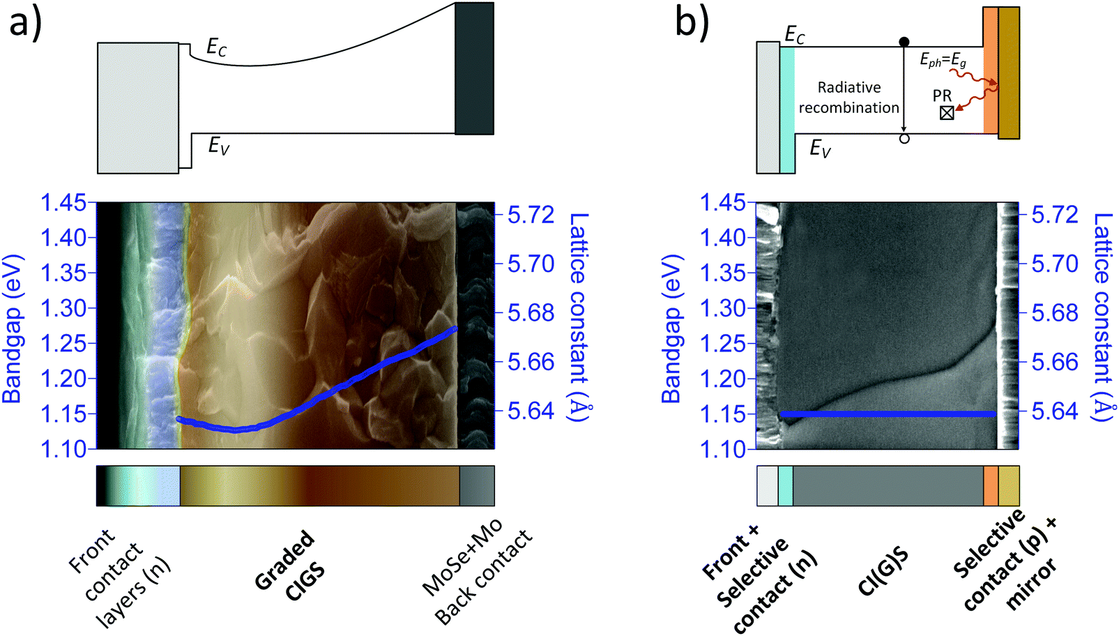 | ||
| Fig. 1 Simplified sketch of band diagrams in the flat-band condition of solar cell designs (top) with corresponding SEM images (bottom). (a) Conventional design with ZnO(Al)/ZnO/CdS front contact layers and (b) idealized proposed concept showing: the (1) non-graded thinner absorber with larger grain size shown in the SEM image, (2) selective contacts at the back and the front and (3) back reflector. A possible photon recycling mechanism is also depicted, initiating from photon emission upon a radiative recombination event, reflection at the back contact and finally reabsorption in the absorber. | ||
Structural defects
As detailed later in this section, the bandgap grading is tailored to improve the device performance via the minimization of recombination at the surfaces/interfaces; however, chemical grading, e.g. by varying the [Ga]/([Ga] + [In]) ratio (GGI), induces strain that relaxes at grain boundaries, limits the grain growth and leads to the formation of structural defects. Specific to the multistage co-evaporation method, the concentration of 1-D and 2-D defects is drastically reduced during a deposition phase in the presence of Cu2−xSe phases. These phases act as a sintering agent that does not uniformly wet the CIGS surface and leads to lateral non-uniformities in composition and to formation of voids (missing material) inside the absorber.13 The crystal quality of the absorber can be improved by inhibiting the formation of voids, horizontal grain boundaries and of 1-D and 2-D defects inside the grains.13,14 This is of special importance during the third stage of the co-evaporation method, in which many of the aforementioned issues arise. Different methods have shown promising results in that respect: alkali post-deposition treatment,3 Ag alloying,15 or sulfurization and selenization methods.10,11 It also seems relevant to modify the growth conditions to prevent formation of these defects. For example, pushing the composition closer to stoichiometry hinders the formation of anti-site defects and reduces bond length variations.16 Indeed, improved efficiency was recently demonstrated for CuInSe2 solar cells with near-stoichiometric composition together with the supply of heavy alkalis (e.g. RbF).17 Additionally, due to the implications of composition gradients for the generation of strain and defects,18 their replacement also emerges as a plausible pathway to enhance the properties of the absorber.Bandgap grading implications for the solar cell performance
The absorber of high efficiency CIGS solar cells is composed of an engineered double bandgap grading across the layer with increasing bandgap towards the back and front surfaces.19 The grading is beneficial to avoid interface recombination at the front, but more importantly at the back interface. Front recombination is mainly lessened by the presence of a CdS layer forming the heterojunction.5 For back recombination, the back bandgap grading acts as an efficient barrier for minority carriers, thus preventing voltage losses.20 Although effective in reducing back interface recombination, it is still not clear if it is completely avoided. Even more importantly, to what extent the back grading influences the effective lifetime of the absorber is also unclear. Within this context, the bandgap grading could exhibit two opposite effects, and this will be analyzed below.We assess here the effect of the back grading on VOC with a numerical model implemented in the Sentaurus tool from Synopsis21 (further details can be found in the numerical simulation section of the ESI†). A baseline simulation with a graded absorber resembling state-of-the-art CIGS solar cell performance22 is implemented with doping level NA = 1016 cm−3, a thickness of 2.5 μm and a minimum GGI of 0.2. The recombination velocity at the CIGS/Mo interface (Sback) is set to infinity (i.e. Sback ≫ 107 cm s−1). The CIGS absorber is divided into two regions: (1) front grading + the so-called notch (R1) and (2) the back grading (R2). The back grading height is characterized by ΔGGI, defined as the difference between the minimum and maximum GGI, as illustrated in the inset at the bottom right of Fig. 2 together with R1 and R2. Several grading slopes corresponding to different ΔGGI values were simulated to evaluate their impact on VOC. Back recombination is highly dependent on the carrier diffusion length (LD), which is related to the carrier lifetime and mobility by the well-known expression LD = (τeμekT/q)1/2. Therefore, a wide range of diffusion length (1 < LD < 50 μm) is also examined by varying the effective minority carrier lifetime (τe) – through the non-radiative lifetime, τnr – and the minority carrier mobility (μe). We choose values for the lifetime and mobility covering a wide range around the expected or reported values in state-of-the-art CIGS.2,4,5,11
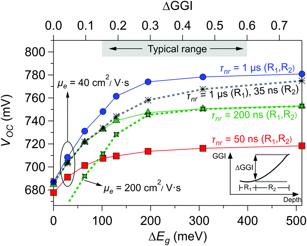 | ||
| Fig. 2 Numerical simulations of VOC as a function of ΔEg (and ΔGGI) between the bandgap minimum and the value at the back of the CIGS layer, for different minority carrier non-radiative lifetime and mobility. The inset shows an example of a GGI absorber gradient; it defines the ΔGGI quantity and separates the absorber into front (R1) and back regions (R2). The back region (R2) starts at 1.2 μm where JSC > 98%, i.e. R1 is almost optically inactive (see the ESI,† Fig. S1). Different ΔGGI heights are evaluated with constant absorber depth. The range for ΔGGI values typical of high efficiency devices is shown in gray. The gray dashed line with asterisk symbols results from unequal uniform properties τnr in the front (R1, 1 μs) and the back grading (35 ns). The green dashed line corresponds to higher carrier mobility (200 cm2 V−1 s−1) than the other cases (40 cm2 V−1 s−1) for τnr = 200 ns in both regions. Lines are a guide to the eye. | ||
Fig. 2 shows VOC as a function of ΔGGI for different τnr and μe. A first important conclusion can be drawn: under the assumption of uniform and equal properties for R1 and R2 (curves with solid lines and symbols), ΔGGI > 0.3 (or ΔEg > 200 meV) is required to prevent most of the back recombination, independently of the lifetime evaluated (50, 200 and 1000 ns2,4,5,11). For the largest ΔGGI investigated, the back grading is already preventing all recombination at the back, i.e. VOC (Sback = ∞) = VOC (Sback = 0) (not shown).
In the presence of interface recombination, VOC also depends on the minority carrier mobility, whose value is not straightforward to determine experimentally. Therefore, in addition to the case evaluated before (μe = 40 cm2 V−1 s−1![[thin space (1/6-em)]](https://www.rsc.org/images/entities/char_2009.gif) 23), we consider μe = 200 cm2 V−1 s−1 (also a reasonable value for CIGS24) and the extreme case of μe = 4000 cm2 V−1 s−1 as an upper limit of our analysis. For μe = 200 cm2 V−1 s−1 and a 200 ns non-radiative lifetime, a similar ΔGGI threshold (∼0.4) is identified to effectively avoid back recombination, as shown by the green dashed line and cross symbols. For μe = 4000 cm2 V−1 s−1 (not shown), the ΔGGI threshold is close to 0.5. Although these instances shift the ΔGGI threshold to avoid recombination at the back, it is still possible to achieve it experimentally. Accordingly, we can state that a sufficient back grading is beneficial to avoid voltage losses at the back for a wide range of lifetime and mobility that could be found in state-of-the-art solar cells.
23), we consider μe = 200 cm2 V−1 s−1 (also a reasonable value for CIGS24) and the extreme case of μe = 4000 cm2 V−1 s−1 as an upper limit of our analysis. For μe = 200 cm2 V−1 s−1 and a 200 ns non-radiative lifetime, a similar ΔGGI threshold (∼0.4) is identified to effectively avoid back recombination, as shown by the green dashed line and cross symbols. For μe = 4000 cm2 V−1 s−1 (not shown), the ΔGGI threshold is close to 0.5. Although these instances shift the ΔGGI threshold to avoid recombination at the back, it is still possible to achieve it experimentally. Accordingly, we can state that a sufficient back grading is beneficial to avoid voltage losses at the back for a wide range of lifetime and mobility that could be found in state-of-the-art solar cells.
Heretofore, it seems that the back grading only brings positive effects on VOC. However, let us recall that we made the assumption of uniform carrier properties throughout the absorber (R1 and R2). In practice, it is reasonable to expect a lower material quality in the back grading region, as the presence of strain and higher Ga content give rise to point defects, dislocations, lower grain size, and defect levels appearing in the band gap, among other effects.25,26 Indeed, the degraded quality of high-Ga content CIGS might also explain the comparatively poorer performance of Ga-rich devices with bandgap above ∼1.15 eV. Accordingly, we now make the assumption of unequal carrier lifetimes for R1 and R2, i.e. 1000 ns and 35 ns (gray dashed line and asterisks), respectively. This means a very high material quality of the notch together with a defective back grading. This assumption is also capable of providing virtually the same VOC (740 mV) and similar efficiency as the baseline structure detailed before, see the gray dashed line (and asterisks) and green triangles at GGI = 0.2. Although this contributes to ambiguity because more than one set of material parameters could reproduce the same results, it also means that the back grading can limit the performance of a notch region with very high quality. The limitation is illustrated by the underperformance of the gray dashed line (and asterisks) compared to the instance with higher lifetime in the back grading (blue curve and filled circles), even for the highest ΔGGI analyzed. Therefore, ΔGGI ∼ 0.5 is enough to avoid recombination at the back interface, but not in the defective back grading region, which reduces the effective lifetime of the CIGS absorber, and thus VOC.
To summarize this section, there is no doubt that the back grading is effective in reducing back recombination. Nevertheless, it comes with several drawbacks. It could alter the device performance by increasing recombination in absorber regions with lower structural and electronic quality, as highlighted by our simulations. It adds complexity to the growth procedure, i.e. it is not easy to tune and control the bandgap profile. Moreover, a graded structure is rather more complicated to model and characterize.
Accordingly, we suggest the use of non-graded absorbers as a pathway towards the next generation of CIGS solar cells with thinner structures and very high efficiencies. A non-graded absorber would simplify the structure, reduce material consumption and overcome some of the VOC limitations. The candidates to substitute the back grading are p-type charge selective contacts, whose suitability has been demonstrated in other technologies, e.g. III–V. Materials are required with pronounced charge selectivity and low interface recombination velocity and which do not affect the absorber properties. Possible implementations are reviewed in section Selective/passivating contacts.
Electronic properties and material quality
In a solar cell of a specific bandgap, the open circuit voltage is directly linked to the bulk electronic properties or the absorber material quality. The CIGS bulk material quality is mainly affected by non-radiative recombination at the grains and/or grain boundaries and by potential fluctuations.27,28 In addition, the absorber might also be influenced by the surrounding interfaces or even by the presence of a defective back grading, as shown in the previous section. Different metrics are usually employed to evaluate the quality of the absorber and interfaces, namely, the external radiative emission efficiency or the so-called VOC deficit (or bandgap–voltage offset, WOC, as used in the III–V field29). Moreover, the minority carrier lifetime is used as a direct parameter to assess the quality of the absorber.23To illustrate the present quality of CIGS solar cells with such metrics, Fig. 3 shows a compilation of efficiencies and VOC deficits (VOC,def = Eth/q − VOC) as a function of the estimated external radiative emission efficiency (ERE).1 The ERE is defined as the ratio of the radiative recombination current with respect to the dark recombination current. It is a good figure of merit because it measures how far VOC is from its radiative limit.30 GaAs and GaInP data are also displayed for comparison purposes. As can be seen, the efficiency is strongly correlated to the ERE and VOC,def measured in different solar cells over the years. An impressive low VOC,def has been measured for CIGS state-of-the-art materials with values ∼350 mV to 400 mV,1,4,11,22,31,32 whereas for the best GaAs6,7 and GaInP33 materials these values are ∼300 mV and ∼350 mV, respectively. These seem impressive values for CIGS, especially because the current structure does not get the same photon recycling benefits as GaAs and GaInP by use of a highly reflective back contact (i.e. gold). To what extent the difference between GaAs and CIGS has to do with the presence of photon recycling or material quality is analyzed in the next section.
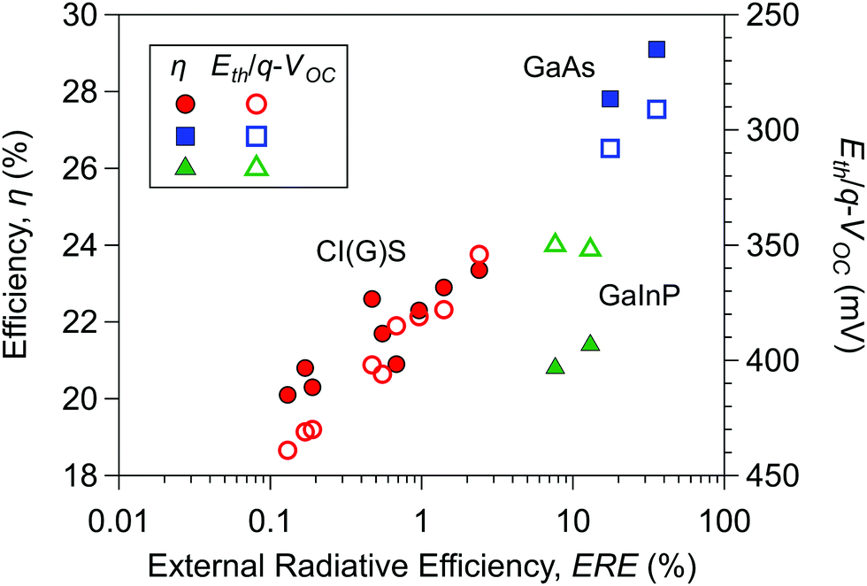 | ||
| Fig. 3 Efficiency (filled symbols) and VOC deficit (open symbols) as a function of ERE (calculated from VOC) for CIGS. III–V devices with a strong impact of photon recycling are also depicted. Eth corresponds to the photovoltaic bandgap definition proposed by Rau et al.30 The same definition is used to compute VOC,def, not included in ref. 1. Data from Green et al.1 were used completed with additional data for GaInP and GaAs from ref. 7 and 33. | ||
Regarding carrier lifetimes, effective values up to 400 ns were reported4 for CIGS (an estimated 350 ns for the non-radiative component), the estimated radiative lifetime being on the order of microseconds.34 For GaAs and GaInP, the highest non-radiative minority carrier lifetimes reported are ∼1 μs to 4 μs (n-type absorber) and 450 ns (p-type absorber), respectively.35–37 For III–V materials, the largest improvement reported due to photon recycling (ΔVOC ∼ 70 mV) was achieved with n-type absorbers, consistent with the higher lifetimes measured (see for example the GaAs case35,38). Although determination of the carrier lifetime in CIGS absorbers is influenced by many factors, which contribute to ambiguity to a certain degree, the low VOC deficit and increased ERE (recent absolute PL experiments confirm 1% ERE in a state-of-the-art CIGS material39) support the high quality of the material.
CIGS solar cells operating in the radiative limit
Conceptually, an ideal solar cell is comprised of a semiconductor (absorber) surrounded by materials (transparent to the incident light) that enable efficient charge separation, i.e. selective contacts.40 In addition, a high degree of light confinement is desired to promote the re-absorption of emitted photons by radiative recombination.41 These two concepts are discussed below, also illustrated with a numerical model implemented in the Sentaurus tool from Synopsis21 (further details are provided in the ESI†).Selective/passivating contacts
In a typical CIGS solar cell, charge separation is usually accomplished by a p–n junction at the front and assisted by the back bandgap grading. Moving towards the replacement of the back grading and the enhancement of the front interface requires the use of selective contacts. The ideal situation would be chemical and/or electrical surface passivation working as an efficient blocking barrier for minority carriers (>300 meV), and a non-blocking interface for majority carriers towards the contacts. For the front contact, n-type materials are readily available42 and some others are under investigation to offer a broader range of possibilities.43 Further surface passivation was also demonstrated by alkali PDT or sulfurization processes.11 For the rear contact, there are no suitable p-type materials readily available, to our knowledge. Promising results for back surface passivation were achieved by the use of different approaches based on atomic layer deposition techniques of different materials.44 It could be also considered to tune the band offsets of CIGS by alloying, for example with Ag.45 The use of III–V materials was also proposed as a possible route for selective contacts.46 Recently published theoretical studies and methods to test charge selectivity would be useful for screening of new selective contacts for CIGS.47,48 A scalable and cost-effective implementation scheme still has to be envisaged.Photon recycling assessment
In general, photons emitted upon radiative recombination travel in random directions and can be re-absorbed in the same layer or in any other adjacent semiconductor layer in the structure with equal or lower bandgap. If the re-absorption takes place in the same layer as emission, the process is known as photon recycling (PR) or self-absorption. It was demonstrated that PR is the key factor for the development of record efficiency solar cells (GaAs-based) operating close to the theoretical limit.6,7 The general implication of PR is that re-absorbed photons increase the radiative lifetime, and thus VOC.49 PR brings its full benefits if the non-radiative recombination rate is minimized and the optical structure is adapted to accomplish a high degree of re-absorption of photons.We extend the model developed in the previous section to estimate the effects of PR on the solar cell performance. The Sentaurus model is adapted to account for the effective increase in the radiative lifetime due to PR. A good approximation is obtained by calculating a photon recycling factor, φ38 (or re-absorption probability,  7), which influences the bimolecular radiative coefficient B, following the methodology of Steiner et al.7 and Lumb et al.38 The photon recycling factor or
  (in principle, equivalent quantities38) depends on the geometry, the angle and the wavelength-dependent Fresnel coefficients at the front and back of the structure7 (further details can be found in the ESI† and Fig. S2). This quantity is used to modify the net radiative lifetime as τr−1 =1 − φ/τ0r,38τ0r being the initial radiative lifetime with no changes due to PR. Then, an effective radiative coefficient (Beff) is used as input in the numerical simulator, computed by the inverse of the product of the doping concentration and the modified radiative lifetime. Therefore, the higher the photon recycling factor (or re-absorption probability) the higher the radiative lifetime and the lower Beff. Although the approaches from ref. 7 and 38 consider flat quasi-Fermi levels along the absorber and neglect the voltage dependence of PR, they have shown as good results as other more rigorous treatment of PR.38,50 In addition, they only require knowledge of the refractive index of the materials, which in the case of CIGS is taken from Carron et al.51 It is worth mentioning here that if the influence of the absorber thickness is neglected in the calculation of Beff (here accounted for in the calculation of
  ), the Sentaurus model would provide a similar trend to the standard Shockley model in which the radiative current increases indefinitely with thickness. In the presence of photon recycling this is not true, and the radiative current saturates at a specific thickness due to the high degree of re-absorption of photons, as advised and demonstrated by Martí et al.49 This is important because Beff needs to be adapted for the simulated structure described below, being different than the one analyzed previously.
The simulated structure including PR effects is composed of a non-graded 1 μm-thick absorber with Eg = 1.14 eV and uniform doping concentration (NA = 1016 cm−3). Charge selective contacts are simulated as ideal minority carrier blocking layers (>300 meV) and ideal current flow for majority carriers with no interface defects. Series resistance is neglected (i.e. influence of grids, interfaces, etc.). Band tails are considered by modifying the absorption coefficient with an exponential Urbach tail with a characteristic energy of 17 meV. This value is larger than experimental observations on high quality CIGS layers,52 but helps to exemplify the effects of band tails on PR. In the simulations, the back contact reflectance was effectively tuned by changing the back layer material (here Mo or Au) to illustrate its influence on photon recycling. A practical implementation of a highly reflective back contact would differ; however it is possible to achieve it experimentally.
Simulations as a function of the material quality (i.e. τnr) of the absorber were performed. Fig. 4 shows VOC,def for device designs considering band tails – or not – and for different reflectance at the back, i.e. molybdenum (integrated R ∼ 30%) and gold (integrated R > 90%). In general, all designs show VOC,def decreasing with a non-radiative lifetime increase until it starts to reach saturation when recombination becomes radiatively limited (τr < τnr). At this point, it is only possible to enhance the performance by increasing the average  assisted by the back reflector. Indeed, it is only in the instance of no tails and
  > 90% (i.e. a gold back reflector) in which VOC is similar to the radiative limit.53 Although not shown in Fig. 4, the FF is also boosted by the increase of the non-radiative lifetime for all cases shown here, as expected.
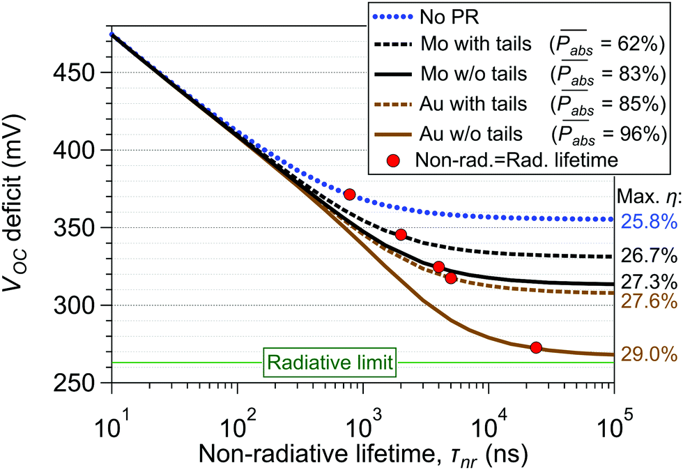 | ||
| Fig. 4 V OC,def as a function of non-radiative lifetime for different average reflectance properties at the back, i.e. molybdenum (R ∼ 30%) and gold (R > 90%), and no photon recycling consideration (No PR). The maximum achievable efficiency (i.e. at τnr = 100 μs) is shown on the right side of the graph. | ||
Let us consider the case of molybdenum and band tails (black dashed line). If non-radiative recombination is kept equal (e.g. τnr = 200 ns) and the presence of photon recycling is high by maximizing  (i.e. gold and no band tails) a marginal VOC gain <5 mV is obtained. This is important because it lies close to VOC,def = 400 mV, which most conventional CIGS solar cells exhibit. In other words, in this scenario the development of a near ideal back reflector would be meaningless for VOC enhancement purposes.
Let us now consider VOC,def = 354 mV, as recently achieved by Solar Frontier.1 This value can be explained by considering photon recycling, or not – for example, the black dashed line at τnr = 1 μs (PR on), or the blue curve with filled circles at τnr > 5 μs (PR off), respectively. If PR is not considered, the recombination in the solar cell must be dominated by the radiative component because τnr > τr. If radiative recombination is dominant, PR effects should become noticeable. Moreover, there is a relatively high re-absorption probability (∼50%, not shown) in a 1 μm-thick CIGS material even by considering a very low reflectance at the back (R < 1%). Therefore, ignoring PR is an unphysical assumption. For high material quality, i.e. record CIGS materials or τnr > τr, the influence of PR on the effective lifetime must be taken into account.
Whereas our simulations required very high quality (τnr > 1 μs) to match the VOC,def of record solar cells, other sets of parameters may also achieve the same results. For example, a different doping concentration – difficult to estimate in CIGS – than the one used for these simulations could modify the calculated values and match the VOC,def even without the need to consider PR and a high τnr (see Fig. S3, ESI†). Despite these complex ambiguities, we can extract one main conclusion: the material quality of state-of-the-art CIGS is close to that required to significantly boost VOC by PR.
It is also clear from Fig. 4 that band tails have an impact on  and consequently on the maximum conversion efficiency. Band tails arise mainly from potential fluctuations present at the conduction and valence bands. The presence of tails limits the benefits of PR because of non-negligible photon emission below the bandgap for which re-absorption is weak.54 However, there are promising indications for band tail reduction. For example, Wolter et al. found that the Urbach energy is lowered down to 10 meV to 12 meV by alkali PDT, significantly lower than the value chosen here (17 meV).52 In addition, a decrease in potential fluctuations after sulfurization processes10 and increased CGI32 were reported. All these effects related to growth conditions and processes are not only beneficial for band tail reduction, but also contribute significantly to the minimization of non-radiative losses. In particular, the role of alkalis could be considered vital to achieve such positive effects.55
Once the non-radiative lifetime becomes higher than the radiative lifetime, a back reflector becomes necessary to further increase VOC. In theory, a very high reflectance is required (R ≫ 90%41) to bring VOC to its fundamental limit. This is difficult to realize in practice; nevertheless, possibilities are being explored. For example, Bissig et al. reported an average back reflectance >60% by implementing a multilayer stack including TCO, Al and Mo56 with no evidence of non-ohmic contacts on state-of-the-art CIGS solar cells. Back reflectors with very high reflectance were also integrated into ultrathin solar cells.57
Finally, the degree of photon recycling can be evaluated by dedicated experiments. Let us begin with a brief description of how photon recycling has been assessed in III–V semiconductors prior to detailing the experiments for CIGS. In III–V technology, it is feasible to realize different layer structures to modulate the level of photon recycling. For instance, the effects of photon recycling can be observed by the use of double heterostructures with different absorber doping concentrations and thicknesses and characterization of the carrier lifetime and surface recombination velocity.35,58,59 Another possibility is to vary the degree of back reflection by growing absorbing layers (i.e. GaAs) with different thicknesses at the back of the structure, or comparing structures with and without an absorbing substrate.7,37 As opposed to III–V technology, those possibilities are not straightforward to realize in state-of-the-art graded CIGS. One possible route is the use of ungraded absorbers – avoiding any possible influence of the back grading on the absorber – with both interfaces passivated with dielectric layers. Al2O3 is a good candidate because it provides good interface passivation (Sback < 50 cm s−160). The level of photon recycling can be then modulated by modifying parameters such as the reflection at the back interface and absorber thickness. Therefore, measuring the minority carrier properties (i.e. TRPL + absolute PL) in such structures can provide insight into the impact of photon recycling on CIGS. Relatively thick layers of the dielectric may be required to ensure good passivation properties, such that implementation of the findings into solar cell devices must be carefully devised. The sequential process can be the following: (1) growth of ungraded absorbers on glass and molybdenum, (2) deposition of Al2O3 layers on the front surface, (3) delamination from the molybdenum and (4) deposition of Al2O3 on the back of the structure. The reflection at the back can be varied to a certain degree by the deposition of various materials to effectively modulate the photon recycling probability. Back graded absorbers can be employed to assess if the compositional gradient negatively affects the bulk material quality.
CIGS with respect to III–V solar cells
Several challenges faced by CIGS are already successfully met by III–V technology; however, the implemented solutions may not be directly transferable to CIGS. For example, efficient back reflectors are readily available for III–V absorbers. GaAs solar cells are grown on a substrate that can be removed to apply a back reflector. This is typically accomplished by epitaxial lift-off, followed by evaporation of metals (typically gold) providing both an average back reflectance higher than 90% and very good ohmic contacts.61 For CIGS, a comparable approach was never deemed attractive from the manufacturing perspective. Instead, combinations of TCO, metal and/or oxide layers have shown promising results,56,57 suggesting that highly reflective and ohmic contacts may be implemented in high-performance devices. Another challenge is the availability of charge selective contacts. Such contacts can be realized with III–V technology by growing epitaxial materials with wider bandgaps, appropriate band offsets and low interfacial recombination velocities (typically well below 100 cm s−162). For CIGS, only a few reports treating selective contacts and interface recombination (especially front recombination) are available,11,23 as commented on in the previous sections. Another difference is related to the doping concentration. A higher doping level increases the quasi-Fermi level splitting, and thus VOC (see Fig. S3, ESI†), as long as the carrier lifetimes and LD remain unaffected. However, doping is difficult to control in CIGS as it depends on a combination of the composition, Cu/III ratio, intrinsic defects, impurities (e.g. Na) and PDT. In III–V, n- and p-type doping can be achieved by controlled incorporation of dopants (e.g. Si and Zn for high material quality) in a wide concentration range (typically in the 1017 cm−3 range) before negatively influencing the carrier lifetime. Finally, non-radiative lifetimes on the order of microseconds are a reality in III–V.35,37 Our simulations suggest that the non-radiative lifetime associated with record CIGS (i.e. VOC,def ∼ 350 mV) is not far from III–V, and it is taking advantage of photon recycling. This is yet to be confirmed experimentally.
Conclusions
We have described the main challenges of CIGS technology related to absorber layer properties and device architecture for next generation solar cells. Potential for a 29% power conversion efficiency is estimated, driven by a boost in VOC and the fill factor. We have identified three main requirements for reaching higher efficiencies: (1) minimization of non-radiative recombination τnr > τr; (2) increased reflectance at the back contact > 90% and 3) reduction of band tails. The question is: how can these requirements be met in practice?The minimization of non-radiative recombination is crucial and some pathways are already under scrutiny by the community. From the material point of view, reduced strain, larger grains, passivated grain boundaries, a lower density of in-grain defects and a lower magnitude of potential fluctuations are desired. Treatments with heavy alkalis contribute to addressing many of these challenges in a remarkable manner. Selenization and sulfurization processes were successful for decreasing non-radiative recombination and potential fluctuations. Ag alloying also offers potential to modify band edges, increase the grain size and reduce the density of structural defects. We have suggested the growth of absorbers with composition close to stoichiometry to reduce the anti-site defect density and bond length variations. In addition, an absent or weaker compositional back grading should help to relieve the strain in the absorber and improve the material quality. This in turn requires the implementation of charge selective contacts, for which different options are already under study.
The improvement in the carrier lifetime, external radiative efficiency and VOC deficit over the last few years has reached the point for which alternative device architectures can benefit from a VOC boost induced by photon recycling. If the non-radiative lifetime is comparable to or higher than the radiative one, an efficient back reflector is essential to take advantage of photon recycling by maximizing re-absorption of photons emitted by radiative recombination. Multilayer thin-film stacks have shown promising results towards very high back reflectance. The implementation of such back reflectors for a VOC increase only becomes important if the VOC deficit is close to or higher than 350 mV, a value that is reached in the current record solar cell. According to our simulations, the CIGS record solar cell is already taking advantage of photon recycling, even in the presence of a possible negative impact of the back grading. A relevant implication is that photon recycling effects must be taken into account for modeling and characterization of state-of-the-art CIGS. Moreover, we have also illustrated that realistic sub-bandgap tails affect the photon reabsorption probability, but still allow for VOC and efficiency values significantly higher than state-of-the-art devices.
From our perspective, this work demonstrates several reasons to foster different strategies in the fabrication methods and device architecture for the next efficiency leap in CIGS solar cells.
Conflicts of interest
There are no conflicts to declare.Acknowledgements
This work received financial support partially from the Swiss State Secretary for Education, Research and Innovation (SERI) under contract number 17.00105 (EMPIR project HyMet) and from the Swiss Federal Office of Energy (SFOE) (SI/501614-01 “ImproCIS”). The EMPIR programme is co-financed by the Participating States and by the European Union's Horizon 2020 research and innovation programme. The authors acknowledge T. Feurer and J. Löckinger for valuable conversations and SEM images of Fig. 1.References
- M. A. Green and A. W. Y. Ho-Baillie, ACS Energy Lett., 2019, 4, 1639–1644 CrossRef CAS.
- M. Nakamura, K. Yamaguchi, Y. Kimoto, Y. Yasaki, T. Kato and H. Sugimoto, IEEE J. Photovoltaics, 2019, 9, 1863–1867 Search PubMed.
- A. Chirilă, et al. , Nat. Mater., 2013, 12, 1107–1111 CrossRef PubMed.
- T. Feurer, et al. , Thin Solid Films, 2018, 670, 34–40 CrossRef.
- T. P. Weiss, et al. , Sci. Technol. Adv. Mater., 2019, 20, 313–323 CrossRef CAS PubMed.
- B. M. Kayes, et al. , IEEE Photovoltaic Spec. Conf., 2011, 000004 Search PubMed.
- M. A. Steiner, J. F. Geisz, I. García, D. J. Friedman, A. Duda and S. R. Kurtz, J. Appl. Phys., 2013, 113, 123109 CrossRef.
- L. M. Mansfield, et al. , IEEE J. Photovoltaics, 2014, 4, 1650–1654 Search PubMed.
- R. Kamada, et al. , IEEE Photovoltaic Spec. Conf., 43th, 2016, 1287–1291 Search PubMed.
- S. Kim, et al. , Jpn. J. Appl. Phys., 2018, 57, 085702 CrossRef.
- T. Kato, J. Wu, Y. Hirai, H. Sugimoto and V. Bermudez, IEEE J. Photovoltaics, 2019, 9, 325–330 Search PubMed.
- J.-F. Guillemoles, T. Kirchartz, D. Cahen and U. Rau, 2019, arXiv:1903.11954v1.
- E. Avancini, et al. , Sci. Technol. Adv. Mater., 2018, 19, 871–882 CrossRef CAS PubMed.
- R. Mainz, et al. , Energy Environ. Sci., 2016, 9, 1818–1827 RSC.
- P. Erslev, G. M. Hanket, W. N. Shafarman and D. J. Cohen, MRS Proc., 2009, 1165, 1165 Search PubMed.
- E. Haubold, et al. , J. Alloys Compd., 2019, 774, 803–812 CrossRef CAS.
- T. Feurer, et al. , Adv. Energy Mater., 2019, 9, 1901428 CrossRef.
- S. Siebentritt, M. Igalson, C. Persson and S. Lany, Prog. Photovoltaics Res. Appl., 2010, 18, 390–410 CrossRef CAS.
- A. Chirilă, et al. , Nat. Mater., 2011, 10, 857–861 CrossRef PubMed.
- T. Dullweber, et al. , Thin Solid Films, 2001, 387, 11–13 CrossRef CAS.
- Synopsys, “Sentaurus Device User Guide.” p. version P-2019.3, 2019.
- T. M. Friedlmeier, et al. , Thin Solid Films, 2017, 633, 13–17 CrossRef CAS.
- T. P. Weiss, B. Bissig, T. Feurer, R. Carron, S. Buecheler and A. N. Tiwari, Sci. Rep., 2019, 9, 5385 CrossRef PubMed.
- H. Hempel, et al. MRS Spring Symposium, Phoenix, 2019, p. Tutorial afternoon session ES20.
- J. Dietrich, D. Abou-Ras, T. Rissom, T. Unold, H. W. Schock and C. Boit, IEEE J. Photovoltaics, 2012, 2(no. 3), 364–370 Search PubMed.
- W. Witte, et al. , Prog. Photovoltaics Res. Appl., 2015, 23, 717–733 CrossRef CAS.
- H. Guthrey, J. Moseley, J. Nishinaga, H. Shibata, H. Takahashi and M. Al-Jassim, IEEE J. Photovoltaics, 2018, 8, 1–8 Search PubMed.
- U. Rau and J. H. Werner, Appl. Phys. Lett., 2004, 84, 3735–3737 CrossRef CAS.
- R. R. King, et al., 24th Eur. Photovolt. Sol. Energy Conf. 2009, 21–25 Sept., 2009, Hamburg, Ger., pp. 55–61.
- U. Rau, B. Blank, T. C. M. Müller and T. Kirchartz, Phys. Rev. Appl., 2017, 7, 044016 CrossRef.
- P. Jackson, R. Wuerz, D. Hariskos, E. Lotter, W. Witte and M. Powalla, Phys. Status Solidi RRL, 2016, 10, 583–586 CrossRef CAS.
- R. Carron, et al. , Adv. Energy Mater., 2019, 1900408 CrossRef.
- J. F. Geisz, M. A. Steiner, I. García, S. R. Kurtz and D. J. Friedman, Appl. Phys. Lett., 2013, 103, 041118 CrossRef.
- J. H. Werner, J. Mattheis and U. Rau, Thin Solid Films, 2005, 480–481, 399–409 CrossRef CAS.
- G. B. Lush, Sol. Energy Mater. Sol. Cells, 2009, 93, 1225–1229 CrossRef CAS.
- R. Dagan, Y. Rosenwaks, A. Kribus, A. W. Walker, J. Ohlmann and F. Dimroth, Appl. Phys. Lett., 2016, 109, 0–4 CrossRef CAS.
- M. A. Steiner, et al. , IEEE J. Photovoltaics, 2013, 3, 1437–1442 Search PubMed.
- M. P. Lumb, M. A. Steiner, J. F. Geisz and R. J. Walters, J. Appl. Phys., 2014, 116, 194504 CrossRef.
- J. M. Prieto, et al., MRS Spring Symposium, Phoenix, 2019, Paper ES20.09.04.
- U. Wurfel, A. Cuevas and P. Wurfel, IEEE J. Photovoltaics, 2015, 5, 461–469 Search PubMed.
- O. D. Miller, E. Yablonovitch and S. R. Kurtz, IEEE J. Photovoltaics, 2012, 2, 1–27 Search PubMed.
- J. Chantana, Y. Kawano, T. Nishimura, T. Kato, H. Sugimoto and T. Minemoto, ACS Appl. Mater. Interfaces, 2019, 11, 7539–7545 CrossRef CAS PubMed.
- F. Larsson, J. Keller, D. Primetzhofer, L. Riekehr, M. Edoff and T. Törndahl, J. Vac. Sci. Technol., A, 2019, 37, 030906 CrossRef.
- G. Birant, et al. , Appl. Sci., 2019, 9, 677 CrossRef CAS.
- M. Edoff, et al. , IEEE J. Photovoltaics, 2017, 7, 1789–1794 Search PubMed.
- D. Lincot, et al. in 35th European Photovoltaic Solar Energy Conference and Exhibition, 2018, Session 1AO.2.2, 23–28.
- U. Rau and T. Kirchartz, Adv. Mater. Interfaces, 2019, 1900252 CrossRef CAS.
- A. Onno, C. Chen, P. Koswatta, M. Boccard and Z. C. Holman, J. Appl. Phys., 2019, 126, 183103 CrossRef.
- A. Martí, J. L. Balenzategui and R. F. Reyna, J. Appl. Phys., 1997, 82, 4067–4075 CrossRef.
- S. M. Durbin and J. L. Gray, IEEE Trans. Electron Devices, 1994, 41, 239–245 CrossRef CAS.
- R. Carron, et al. , Sci. Technol. Adv. Mater., 2018, 19(1), 396–410 CrossRef CAS PubMed.
- M. H. Wolter, PhD dissertation, University of Luxembourg, 2019.
- T. Kirchartz and U. Rau, Adv. Energy Mater., 2018, 1703385 CrossRef.
- J. Mattheis, U. Rau and J. H. Werner, J. Appl. Phys., 2007, 101, 113519 CrossRef.
- F. Pianezzi, et al. , Phys. Chem. Chem. Phys., 2014, 16, 8843 RSC.
- B. Bissig, et al. , Prog. Photovoltaics Res. Appl., 2018, 26, 894–900 CrossRef CAS.
- L. Gouillart, et al. , IEEE J. Photovoltaics, 2019, 10, 250–254 Search PubMed.
- R. J. Nelson and R. G. Sobers, Appl. Phys. Lett., 1978, 32, 761–763 CrossRef CAS.
- R. King, J. Ermer and D. Joslin, 2nd World Conf. Photovolt. Sol. Energy Conversion, 1998, 86–90 CAS.
- W.-W. Hsu, et al. , Appl. Phys. Lett., 2012, 100, 023508 CrossRef.
- G. J. Bauhuis, P. Mulder, E. J. Haverkamp, J. C. C. M. Huijben and J. J. Schermer, Sol. Energy Mater. Sol. Cells, 2009, 93, 1488–1491 CrossRef CAS.
- S. R. Kurtz, J. M. Olson, D. J. Friedman, J. F. Geisz, K. A. Bertness and A. E. Kibbler., MRS Proc., 1999, 573, 95 CrossRef CAS.
Footnote |
| † Electronic supplementary information (ESI) available. See DOI: 10.1039/d0ee00834f |
| This journal is © The Royal Society of Chemistry 2020 |