
Bifacial passivation of n-silicon metal–insulator–semiconductor photoelectrodes for efficient oxygen and hydrogen evolution reactions†
Bin
Liu
ab,
Shijia
Feng
ab,
Lifei
Yang
c,
Chengcheng
Li
ab,
Zhibin
Luo
ab,
Tuo
Wang
 *ab and
Jinlong
Gong
ab
*ab and
Jinlong
Gong
ab
aKey Laboratory for Green Chemical Technology of Ministry of Education, School of Chemical Engineering and Technology, Tianjin University, Tianjin 300072, China. E-mail: wangtuo@tju.edu.cn
bCollaborative Innovation Center of Chemical Science and Engineering (Tianjin), Tianjin 300072, China
cGCL System Integration Technology Co., Ltd, Suzhou 215000, China
First published on 20th November 2019
Abstract
Silicon-based (Si-based) junctions have been widely investigated in recent years as photoelectrochemical (PEC) water splitting photoelectrodes, including buried junctions and metal–insulator–semiconductor (MIS) Schottky junctions. However, Si-based MIS photoelectrodes suffer from low performance for the PEC oxygen evolution reaction (OER) and hydrogen evolution reaction (HER) because of the dilemma that a thin insulator cannot provide enough interfacial passivation while a thick insulator will block the transport of charge carriers. Another trade-off is the fact that the photovoltage extracted from the band offset between the metal and semiconductor will be counteracted by the parasitic light absorption of the metal layer, sacrificing the saturation photocurrent. This paper describes the design and realization of a bifacial passivation strategy for the metal/Si interface of an MIS photoelectrode, featuring a bi-layer stack consisting of amorphous silicon (a-Si) for passivating the silicon surface and a metal oxide (TiO2) for passivating the metal surface. Upon the bifacial passivation of both a-Si and TiO2, the minority carrier lifetime of the Si MIS photoanode was significantly improved from 18 to 2360 μs. Enabled by this extremely long minority carrier lifetime, it becomes possible to place the MIS junction on the back side of a Si substrate to construct an inverted-MIS (I-MIS) structure to eliminate the parasitic light absorption of traditional Si MIS photoelectrodes. The obtained photoelectrode exhibits an excellent onset potential of 0.85 V and 0.62 V vs. reversible hydrogen electrode (RHE) for the OER and HER, respectively. Eventually, unprecedented applied bias photon-to-current efficiencies (ABPE) of 3.91% and 12.66% were obtained by Si MIS and Si I-MIS, which are the highest among MIS-based photoanodes and photocathodes, with 30 h and 108![[thin space (1/6-em)]](https://www.rsc.org/images/entities/char_2009.gif) h stable operation. When pairing the Si I-MIS photocathode with a BiVO4 photoanode to form a PEC membrane-free tandem cell, an unbiased solar-to-hydrogen conversion efficiency of 1.9% is achieved.
h stable operation. When pairing the Si I-MIS photocathode with a BiVO4 photoanode to form a PEC membrane-free tandem cell, an unbiased solar-to-hydrogen conversion efficiency of 1.9% is achieved.
Broader contextThe excessive exploitation of fossil fuels has brought humankind into a series of crises. Our world is heavily polluted and the energy reserves are exhausted. Fortunately, the sun provides inexhaustible free energy for the earth. Photoelectrochemical (PEC) water splitting is an attractive route to convert solar energy into chemical fuels. Si-based metal–insulator–semiconductor (MIS) Schottky junctions have been widely investigated in recent years as PEC water splitting photoelectrodes. However, Si-based MIS photoelectrodes suffer from low performance for the PEC oxygen evolution reaction (OER) and hydrogen evolution reaction (HER), primarily because the commonly used surface passivation layer could not guarantee a desired Si/metal interface. Taking Si MIS as a prototype, we demonstrate a bifacial passivation strategy for the PEC OER and HER. The bifacial passivation stack (a-Si/TiO2) provides excellent surface and interfacial passivation for both the Si side and metal side of the Si/Ni interface within a thin thickness that allows effective charge transport. As a consequence, the optimized Si MIS photoanode and Si I-MIS photocathode exhibit a record-breaking solar-to-O2 efficiency of 3.91% and solar-to-H2 efficiency of 12.66%. This work presents new insights into the fabrication of state-of-the-art MIS photoelectrodes for efficient solar water splitting. |
1. Introduction
Photoelectrochemical (PEC) water splitting is an attractive route to convert solar energy into chemical fuels. A PEC cell usually consists of a photoactive and durable semiconductor to absorb light and generate electron–hole pairs.1,2 In the last few decades, various semiconductors have been investigated for PEC water splitting such as TiO2,3 Fe2O3,4,5 BiVO4,6,7 monocrystalline silicon (c-Si),8–10 Cu2O,11 CIGS,12,13 and amorphous silicon (a-Si), etc.14 Among them, Si is an attractive candidate owing to its narrow band gap (1.1 eV). It is expected that Si will remain the dominant material for semiconductor and photovoltaic applications in the foreseeable future due to its low cost and other significant advantages, including its abundance, non-toxicity and mature production technologies.15 Until now, the efficiency of silicon solar cells has exceeded 26%.16Buried Si p–n junctions (homojunctions) as PEC electrodes have attracted considerable attention due to their higher photovoltage compared with semiconductor–liquid junctions.17–19 The application of pn+ or np+ junctions as photoelectrodes has been widely investigated,20,21 and some remarkable results have been achieved.8,22,23 However, the fabrication process of p–n junctions requires high temperatures and the doping source (such as POCl3 and PH3) is always of high toxicicty.24,25 Thus, it is highly desirable to develop doping free structures to create band bending and extract minority carriers toward the Si surface.26,27 Recently, Si-based metal–insulator–semiconductor (MIS) structures have attracted increasing attention in PEC water splitting.28 For example, when an n-type semiconductor is in contact with a high work function metal or transition-metal-oxide,29 the electron Fermi level falls close to the valence band at the interface and creates a potential barrier that repels the majority carriers. The barrier height should be closely associated with the work function of the metal relative to the electron affinity of Si according to the Schottky–Mott rule.30 To obtain a high photovoltage, the work function of the metal should be of a high value. Nickel (Ni) is a promising metal due to its high work function, high stability in alkaline solution and its abundance in the earth's crust.31 Kenney and coworkers have reported that a Schottky junction on Si with high performance was created by using a Ni film.32
Despite the great advantages of the MIS structure for PEC water splitting, the MIS structure suffers from low photovoltage and also low saturation photocurrent densities due to the surface carrier recombination of Si. There are two effective ways to reduce the surface recombination velocity. The first is chemical passivation by completing the dangling bonds using a surface dielectric layer or chemical species, and the second is field effect passivation by reducing the density of carriers at the surface of Si.33 Dielectric materials such as hydrogenated amorphous silicon nitride (a-SiNx:H) and aluminum oxide (Al2O3) are widely applied in solar cells as surface passivation layers.34 To provide sufficient surface passivation, the threshold thickness of a-SiNx:H and Al2O3 is 80 and 7 nm,35 respectively. However, the transport of photogenerated carriers relies on the tunneling mechanism in MIS Schottky junctions,36 thus the thickness of the insulator should be less than 3 nm.37 Obviously, Al2O3 and a-SiNx:H with a thickness less than 3 nm cannot provide enough passivation for MIS Schottky junctions. Therefore, it is contradictory to decrease the surface recombination velocity using a thick insulator layer while expecting effective carrier tunneling for Si MIS photoelectrodes. Furthermore, another rarely investigated but critical factor for MIS junctions is the interfacial defects at the metal/semiconductor interface, which significantly affect the barrier height due to the Fermi level pinning caused by the metal layer.31,38 It is urgently needed to realize the simultaneous elimination of both intrinsic defects on the Si surface and the newly formed defects at the metal/semiconductor interface.
Besides low photovoltage, Si MIS electrodes always suffer from low saturation photocurrent densities due to the parasitic light absorption from the metal layers. The metal layer is essential to induce the energy band bending for the semiconductor in Si MIS junctions. Thus, the Si surface should be completely covered by the metal layer to enlarge the Schottky junction area to obtain a uniform distribution of the depletion region. But the photocurrent is highly related to the metal layer thickness. A thinner layer is insufficient to obtain the desired band bending, whereas a thicker layer results in low photocurrent densities. The typical saturation photocurrent of Si MIS photoelectrodes is about 35 mA cm−2. However, compared with the theoretical photocurrent (42.7 mA cm−2) that c-Si can afford,29 there is still plenty of room for MIS photoelectrodes to improve.
This paper describes the design and fabrication of a bifacial passivation layer for Si-based MIS photoelectrodes. Specifically, a 5 nm high-quality amorphous silicon (a-Si) layer and a 1.5 nm TiO2 layer were deposited to passivate the c-Si and metal surface, respectively. Using Ni as a representative metal layer due to its high work function, the bifacial passivation strategy eliminates both surface recombination defects for c-Si and interfacial defects for the c-Si/Ni interface. Upon the bifacial passivation, the photogenerated minority carrier diffusion length of Si was improved from 148 to 1690 μm. As a result, the MIS junction could be moved to the back side of a Si substrate to construct an inverted-MIS (I-MIS) to eliminate the parasitic light absorption of traditional Si MIS photoelectrodes. In consequence, the Si MIS photoanode exhibited a solar-to-O2 efficiency of 3.91%, and a low onset potential of 0.85 V vs. RHE for the OER in 1 M KOH (pH 14), with a photocurrent density of 34 mA cm−2 at 1.23 V vs. RHE. The resulting Si I-MIS photocathode exhibited a solar-to-H2 efficiency of 12.66%, and an onset potential of 0.62 V vs. RHE for the HER in 1 M HClO4 (pH 0).
2. Results and discussion
2.1 Construction of Si MIS photoanodes for the OER
Using Ni to extract minority carriers from n-Si, the Si MIS (a-Si/n-c-Si/a-Si/TiO2/Ni) with a bifacial a-Si/TiO2 passivation layer could be used as the photoanode (Fig. 1a, photograph in Fig. S1a, ESI†). The thickness of the Ni layer was optimized to 2 nm (Fig. S2, ESI†), which serves as a high work function metal layer to induce the band bending (J–V curve of n-Si without Ni in Fig. S3, ESI†), as well as providing protection for the underlying Si. Upon oxidation, Ni partially transforms into NiO and Ni(OH)2 as the OER catalyst, as indicated by X-ray photoelectron spectroscopy (XPS). The O 1s XPS signal could be deconvoluted into two peaks (529.8 and 531.3 eV), while the Ni 2p signal could be deconvoluted into three pairs of doublets (851.6, 852.4, and 854.4 eV), which reveals the co-existence of Ni, NiO, and Ni(OH)2 on the surface of the Si MIS photoanode (Fig. S4, ESI†).31,32 The thickness of the a-Si layer is optimized to 5 nm to ensure adequate surface passivation and maximized fill factor for the Si MIS junction, since a-Si will not provide sufficient surface passivation if the thickness is too thin (lower than 5 nm), while the resistance for charge transport will increase significantly if the a-Si is too thick (higher than 10 nm).39,40 | ||
| Fig. 1 (a) Schematic of the Si MIS photoanode. (b) J–V curves of the Si MIS photoanodes with or without a-Si passivation and the corresponding dark current. (c) ABPE of the Si MIS photoanodes with or without a-Si passivation. (d) Stability test of the Si MIS photoanode. The data in (b–d) were measured in 1 M KOH (pH 14) electrolyte under simulated AM 1.5G illumination. | ||
The J–V curves of the Si MIS photoanode with or without a-Si passivation were evaluated in 1 M KOH (pH 14) (Fig. 1b). The a-Si passivated Si MIS photoanode exhibits an early onset (defined as the potential required to achieve a photocurrent of 0.1 mA cm−2) of photocurrent at 0.85 V vs. RHE, with a large saturation current density (37.5 mA cm−2) and sharp slope. The photocurrent density reaches 34 mA cm−2 at 1.23 V vs. RHE, which is almost the best value among Si-based photoanodes for the PEC OER (Fig. S5 and Table S1, ESI†). When compared with photoanodes composed of many other materials (TiO2, Fe2O3, WO3, BiVO4, and μc-Si), the OER performance of our Si MIS structure is still outstanding (Table S3, ESI†). The photovoltage of the a-Si passivated photoanode is 700 mV, as indicated by the difference in the onset potential between the MIS photoanode and degenerated p+-Si/TiO2/Ni electrode with no photoresponse (Fig. 1b). On the other hand, the Si MIS photoanode without a-Si passivation (n-Si/TiO2/Ni) shows a delayed onset potential of 1.15 V vs. RHE with lower saturation current (30 mA cm-2), similar to the results reported previously,39,40 and the photovoltage of the photoanode without a-Si passivation is only 450 mV (Fig. 1b). The improved PEC performance upon a-Si passivation could be attributed to the fact that surface defects could be largely fixed by a-Si, which could suppress the recombination of photogenerated carriers at the Si surface for efficient charge transport. The applied bias photon-to-current efficiency (ABPE) of the a-Si passivated photoanode reaches 3.91% (Fig. 1c), which significantly surpasses the one without a-Si passivation (0.1%). The stability of the Si MIS photoanode was evaluated at a bias of 1.4 and 1.8 V vs. RHE in 1 M KOH under AM 1.5G illumination. The current density at 1.4 V vs. RHE shows a noticeable decay after 20 h in the stability test (Fig. S6, ESI†). In contrast, the current density at 1.8 V vs. RHE remains stable for over 30 h (Fig. 1d). The surface morphology (Fig. S7, ESI†) and J–V characteristics (Fig. S8, ESI†) of the Si MIS photoanodes are almost unchanged after a 30 h stability test, demonstrating the effectiveness of TiO2 and Ni as the protective layers against corrosion. However, the Si MIS photoanode without the TiO2 layer showed noticeable decay after an 8 h stability test (Fig. S9, ESI†), indicating that the TiO2 could effectively enhance the stability of the Si MIS photoanodes.
To further understand the effect of a-Si passivation on the MIS Schottky junction, Si MIS solid-state devices with and without a-Si passivation were fabricated and measured in the dark (schematic illustration in Fig. S10, ESI†). The a-Si passivated MIS shows a much lower reverse saturation current density (J0) (4 × 10⁻¹⁰ A cm-2) than the MIS without a-Si passivation (3 × 10⁻⁸ A cm-2) (Fig. 2a). To obtain a high photovoltage (Voc) for Si MIS junctions,41,42J0 must be reduced since the leakage current leads to a lower Voc. Thus, the theoretical maximum Voc was calculated according the obtained J0.15 Notably, compared with the Si MIS without a-Si passivation, the a-Si passivated Si MIS exhibits a significantly improved theoretical maximum Voc from 530 mV to 648 mV, indicating that the a-Si passivation layer could effectively improve the photovoltage of the Si MIS junction (calculation details in the ESI†).
 | ||
| Fig. 2 (a) Solid-state J–V curves of the Si MIS with or without a-Si passivation in the dark. (b) Mott–Schottky plots of the Si MIS with or without a-Si passivation in the dark. (c) PL spectra of Si MIS with various passivation layers. (d) EIS Nyquist plots attained at 1.4 V vs. RHE under simulated AM 1.5G illumination. | ||
To investigate the relationship between a-Si passivation and the effective barrier height of the Si MIS junction, the Mott–Schottky (M–S) plot and flat-band potential (Efb) of the Si MIS junction with or without the a-Si passivation layer were obtained29 (Fig. 2b). The theoretical maximum barrier height of the n-c-Si/Ni interface is determined by the offset between the Fermi level of n-Si and the work function of Ni. However, this theoretical barrier height will be fixed by the Fermi level pinning effect, due to the existence of dangling bonds on the Si surface. The a-Si passivated Si MIS presents a higher (0.77 V) effective Efb than the Si MIS without a-Si passivation (0.40 V). The calculated effective barrier height of the Si MIS with or without a-Si passivation is 0.94 and 0.57 V (calculation details in the ESI†), respectively. Such a large effective barrier height of the a-Si passivated MIS would present a large photovoltage, owing to the improved charge separation inside Si (band diagrams in Fig. S11a, ESI†). Thus, a-Si is an effective material to passivate the dangling bonds of the Si surface so that large band bending could be established at the a-Si/Ni interface.
a-Si is an excellent passivation layer for the underlying c-Si substrate. However, a-Si could not guarantee a desired interface with the metallic layer at the a-Si/Ni interface. For a general Si/metal interface, there is a finite density of states throughout the band gap of Si near the interface, or the so-called “metal-induced gap states” (MIGS),31,43,44 which prevents the barrier height from being modulated by the work function of the metal,45 also contributing to the pinning of Fermi levels. Thus, an oxide layer is more desired for the passivation of the Ni layer.46 Atomic layer deposition (ALD) deposited TiO2 was introduced as a secondary passivation layer to passivate the interface between a-Si and Ni without affecting the light absorption of Si (Fig. S12, ESI†). The PEC performance of the MIS photoanodes with various TiO2 thicknesses was evaluated in 1 M KOH (pH 14) under AM 1.5G illumination (Fig. S13, ESI†), which indicates that the MIS photoanode with 1.5 nm TiO2 exhibits the lowest onset potential for the PEC OER. In contrast, the photoanode with thinner (0 or 0.75 nm) or thicker (3 or 4 nm) TiO2 presents a more positive oxidation potential. This optimized 1.5 nm thickness is because TiO2 will not completely fix the positive charges at the interface if the thickness is too thin,29,31 while the tunneling resistance for charge transport will increase significantly if the TiO2 is too thick.46
To evaluate the bifacial passivation of a-Si and TiO2, steady-state photoluminescence spectroscopy (PL) was conducted to examine charge recombination (Fig. 2c). The Si without any passivation layer (pristine Si, black trace) exhibits strong fluorescence, indicating severe charge recombination. In contrast, the intensity of the fluorescence is weakened upon TiO2 or a-Si passivation (green and orange traces). It was also reported that a black Si photoanode exhibited remarkable efficiency using TiO2 as the passivation and protective layer.47 The PL intensity is further reduced upon the deposition of both a-Si and TiO2 (blue trace), which indicates that the defects on both the Si surface and the newly formed a-Si/Ni interface are effectively eliminated simultaneously. It is noteworthy that the reduction of the PL intensity upon inserting TiO2 is more significant for the a-Si/Ni interface than the c-Si/Ni interface, suggesting that while TiO2 might not be a very effective passivation material for the c-Si/Ni interface, it is extremely useful to fix the defects at the a-Si/Ni interface. The MIS photoanode without TiO2 exhibits smaller arcs in the electrochemical impedance spectroscopy (EIS) at 1.4 V vs. RHE (Fig. 2d) compared with the one with TiO2, which reveals that TiO2 indeed hinders the hole transportation, consistent with former investigations.48 This could be attributed to a total thickness of 6.5 nm for the a-Si/TiO2 stack, inhibiting the transportation of charge carriers. However, the resistance for charge transportation by adding the TiO2 layer is compensated by the passivation effect, as the MIS photoanode with the TiO2 layer exhibits much a higher performance than the MIS photoanode without the TiO2 layer (Fig. S13, ESI†). In addition, compared with other metal oxides (such as SiO2 and Al2O3) that may serve as the defect passivation layer, ALD-TiO2 presented much stronger stability in alkaline solution.13,49,50 Thus, TiO2 is selected as the secondary passivation layer to eliminate the presence of MIGS caused by the direct contact between Si and Ni, which ensures optimized overall passivation.
Upon the bifacial passivation of a-Si/TiO2 stack, the minority carrier lifetime of Si MIS is improved from 18 to 2360 μs. The corresponding surface recombination velocity of the Si substrate (288 cm s−1) is reduced by almost 100 times to 3.3 cm s−1 with bifacial passivation (calculation details in the ESI†). Furthermore, the photogenerated minority carrier diffusion length of the Si substrate with bifacial passivation was improved from 148 to 1690 μm, which makes it possible for photogenerated holes to transport through the entire Si substrate (155 μm in thickness) for surface reactions on the backside. Thus, this bifacial passivation strategy enables the decoupling of the light absorption and surface reaction, which opens new flexibility to design efficient photoelectrodes.
2.2 Construction of inverted Si MIS photocathodes for the HER and unassisted water splitting
Despite the acceptable performance and stability achieved by bifacial passivated Si MIS photoanodes, there is still a trade-off between photocurrent and photovoltage (band energy offset). Specifically, the photocurrent of Si MIS significantly decreases with increasing Ni thickness.51 It is difficult for traditional MIS junctions to eliminate this problem. The metal layers are always limited to less than 3 nm for sufficient light absorption.31,32 In this study, the a-Si/TiO2 bifacial passivation layer enables an extremely long minority carrier diffusion length (1690 μm), much larger than the Si substrate thickness (155 μm) (band diagram in Fig. S11b, ESI†). Hence, an original inverted I-MIS (Ni/TiO2/a-Si/n-c-Si/a-Si/ITO/TiO2/Pt) junction is developed for the PEC HER, where the MIS junction was placed at the opposite-side of the solar irradiation (Fig. 3a). Thus, a relatively thick Ni layer (100 nm) at the backside of the I-MIS photocathode could be used to establish a fully developed Schottky junction for improved photovoltage, without sacrificing the photocurrent, since it will not block the absorption of light (photograph in Fig. S1b, ESI†). | ||
| Fig. 3 (a) Schematic of the Si I-MIS photocathode. (b) J–V curves, (c) corresponding ABPE curves and (d) stability test of the Si I-MIS photocathode. The data in (b, c, and d) were measured in 1 M HClO4 (pH 0) electrolyte under simulated AM 1.5G illumination. | ||
With 1.5 nm Pt as the HER catalyst (Fig. S14, ESI†), the photovoltage of the I-MIS photocathode is 620 mV, as indicated by the difference in onset potential between the I-MIS photocathode and degenerated n++-Si/TiO2/Pt electrode with no photoresponse (Fig. 3b). XPS confirms the existence of TiO2 and sputtered Pt on the Si I-MIS photocathode surface (Fig. S15, ESI†). The faradaic efficiency of H2 generation for the Si MIS photocathode is higher than 97% at 0.2 V vs. RHE under AM 1.5G irradiation over a 2 h period, indicating that most of the photogenerated charges are consumed for the HER (Fig. S16, ESI†), achieving an unprecedented ABPE of 12.66% in 1 M HClO4 (pH 0) (Fig. 3c). To the best of our knowledge, this is the highest ABPE efficiency among Si-based MIS photocathodes, surpassing many buried Si p–n junction photocathodes for the PEC HER (Fig. S17 and Table S2, ESI†), and outperforming photocathodes composed of many other materials (CIGS, a-Si, CdTe, GaInP, and Cu2O, Table S4, ESI†). This extremely high ABPE efficiency of the Si I-MIS photocathode is attributed to the high photovoltage provided by the large and uniform I-MIS junction. The Si I-MIS photocathode with an 8 nm TiO2 protective layer was tested under continuous stirring at an applied bias of 0.2 V vs. RHE in 1 M HClO4 (pH 0) solution with 12 h illumination with simulated AM 1.5G, followed by another 12 h idle in the dark, which was repeated 9 times to reach an overall duration of 216 h with 108 h illumination. Impressively, our photocathode is stable over the 108 h illumination (Fig. 3d), and the surface morphology of the electrode is nearly unchanged after the stability test (Fig. S18, ESI†). Grazing incidence X-ray diffraction (GIXRD) exhibits a similar ITO diffraction peak intensity after the 108 h stability test, illustrating the excellent protective effect of the ALD-grown TiO2 layer (Fig. S19b, ESI†). Additionally, the electrode exhibits fast and robust H2 bubble evolution with facile bubble detachment, where bubble accumulation is not observed on the electrode surface (ESI,† Movie).
To illustrate the practical application potential of the Si I-MIS photocathode, unassisted overall solar water splitting is demonstrated using a PEC tandem cell composed of the I-MIS photocathode and a BiVO4/FeOOH/NiOOH photoanode. The J–V curves of BiVO4 and I-MIS (behind BiVO4) are obtained in a three-electrode configuration, respectively, where a theoretical photocurrent of 1.8 mA cm−2 could be expected by the intersection of the two J–V curves (Fig. 4a). The two electrodes were connected in series without external bias to form the tandem cell, with light illuminating from the side of BiVO4 (inset of Fig. 4b). An actual photocurrent of 1.55 mA cm−2 was obtained by the unbiased two-electrode configuration (Fig. 4b), which is smaller than the estimated value of 1.8 mA cm−2. The difference may be due to polarization losses. The solar to hydrogen efficiency calculated from the unassisted two-electrode photocurrent is 1.9%. The decrease of the photocurrent is likely due to a mass transfer issue because the PEC tandem cell in this work is a membrane-free static reactor without continuous stirring to minimize the mixture of H2 and O2,13,52 at the expense of insufficient hydroxyl supply for the photoanode.53 Future study should be focused on the design of a PEC tandem cell which is free of mass transfer and polarization losses.
 | ||
| Fig. 4 (a) J–V curves of the Si I-MIS photocathode (behind BiVO4) and BiVO4/FeOOH/NiOOH under simulated AM 1.5G illumination measured using a three-electrode configuration. (b) J–V curves for the two electrode tandem cell without stirring under simulated AM 1.5G illumination. Electrolyte: 0.5 M potassium bicarbonate aqueous solution (pH 8.5). Inset: Schematic of the BiVO4 photoanode and I-MIS photocathode tandem water splitting cell. | ||
3. Conclusion
This work designs and fabricates Si MIS and I-MIS photoelectrodes with a bifacial passivation layer for the PEC OER and HER, respectively. The bifacial passivation stack (a-Si/TiO2) provides surface and interfacial passivation for both the Si side and the metal side of the Si/Ni interface within a thin thickness that allows effective charge transport. This bifacial passivation strategy overcomes the trade-off between photovoltage and photocurrent of the conventional Si MIS junctions. Specifically, a-Si is introduced as the surface passivation layer to passivate the dangling bonds of the c-Si surface, while TiO2 is inserted as a secondary passivation layer to eliminate the metal-induced gap states at the newly formed a-Si/Ni interface. The obtained Si MIS photoanodes with bifacial passivation present an ultra-low interfacial recombination velocity after being passivated by a-Si and TiO2, which results in a lowest onset potential of 0.85 V vs. RHE and a record high ABPE (3.9%) and shows long stability over 30 h for the PEC OER. Furthermore, an original Si I-MIS was designed as a photocathode to eliminate the trade-off between band bending and light absorption in Si MIS photoelectrodes, achieving a high ABPE of 12.66% and onset potential of 0.62 V vs. RHE, with 108 h stable operation. Additionally, an I-MIS-BiVO4 PEC tandem cell is constructed, achieving a solar to hydrogen conversion efficiency of 1.9% without external bias. This work identifies the important role of surface and interfacial passivation in photoelectrochemical conversion and provides new strategies for the fabrication of state-of-the-art MIS photoelectrodes for efficient solar water splitting.4. Experiment section
4.1 Materials
Potassium hydroxide (KOH, ≥99%) and perchloric acid (HClO4) were purchased from Shanghai Aladdin Industrial Corporation. Titanium(IV) i-propoxide (TTIP, 99.999%) was purchased from Suzhou Fornano Electronics Technology Co. Ltd. High purity water (18.25 MΩ cm) supplied by a UP Water Purification System was used in the entire experimental process. All the reagents were used directly without further purification.4.2 Passivation of the silicon substrate
Czochralski (CZ) n-type c-Si substrates with a resistivity of 1–3 Ω cm, 155 μm thickness and (100)-orientation were used as the substrate. First, the silicon substrate was textured using a mixture of potassium hydroxide (KOH) and isopropyl alcohol (IPA), and then it was cleaned via standard RCA cleaning methods and finally dipped in 5% HF for 60 s to remove the surface native oxide layer. After the cleaning process, the Si substrate was put into a plasma enhanced chemical vapor deposition (PECVD) chamber. a-Si layers with 5 nm thickness were used to passivate the front- and backside surfaces of the substrates. n+-a-Si was deposited on the back surface for field effect passivation. A WCT-120 lifetime tester from Sinton Instruments was used for minority carrier lifetime measurement.4.3 Atom layered deposition (ALD) of TiO2
TiO2 was deposited at 150 °C using TTIP (70 °C) as the titanium source and H2O (25 °C) as the oxidant source through a typical thermal ALD process. One ALD cycle consists of a TTIP dose for 0.3 s, N2 purge for 8 s, water dose for 0.1 s and N2 purge for 8 s. The thickness of the TiO2 film was controlled by the number of cycles.4.4 Characterization
The thickness of the a-Si, TiO2 and Ni layers on the polished Si(100) monitor substrate was obtained using a spectroscopic ellipsometer (M-2000 DI, J. A. Woollam Co., Inc.) at 60° and 70° incident angles, by fitting the amplitude ratio (Ψ) and phase shift (Δ) of polarized light with the Cauchy dispersion model for a-Si and TiO2, and a tabulated metallic Ni model for Ni. The Si monitor substrate was placed 5 mm next to the Si sample in the same batch. The morphology was characterized by field emission scanning electron microscope (FESEM, Hitachi S-4800, 5 kV). XPS analysis was carried out on a Physical Electronics PHI 1600 ESCA system with an Al Kα X-ray source (1486.6 eV). The binding energy was calibrated against the C 1s photoelectron peak at 284.6 eV as the reference. PL spectra were obtained on a Hitachi F-4600 fluorescence spectrophotometer. The optical reflectance measurement of Si was performed using a Shimadzu UV-2550 spectrophotometer. The XRD (D/MAX-2500, Rigaku) spectra were collected over a 2θ range from 20° to 60° at a scanning speed of 0.02° per step.4.5 PEC measurements
PEC measurements were performed using a three-electrode configuration with the prepared electrode as the working electrode, saturated Ag/AgCl as the reference electrode, and platinum foil as the counter electrode. Photographs of the apparatus used in the PEC measurement are shown in Fig. S20 (ESI†). The electrolyte for PEC water oxidation was 1 M KOH aqueous solution (pH 14) and for water reduction was 1 M HClO4 aqueous solution (pH 0). The potentials obtained from each measurement were converted into values against the reversible hydrogen electrode using the Nernst equation, eqn (1).| ERHE(V) = EAg/AgCl + 0.059 × pH + 0.197 | (1) |
The applied bias photon-to-current efficiency (ABPE) of the photocathodes was calculated using the J–V curves with an assumption of 100% faradaic efficiency, according to eqn (2)
 | (2) |
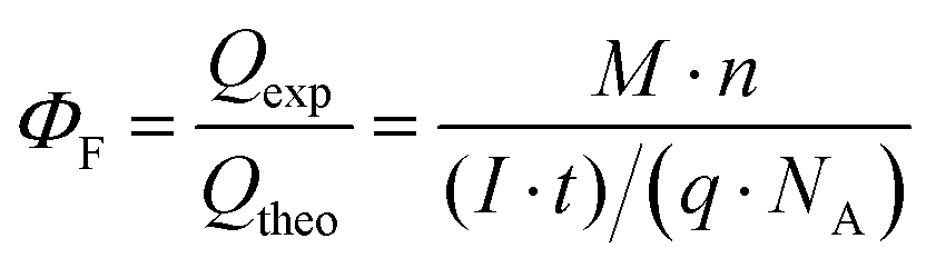
The faradaic efficiency of H2 production for the Si photoelectrodes was calculated according to eqn (3)
 | (3) |
4.6 Magnetron sputtering deposition of the Ni and Pt catalyst
Ni and Pt were both deposited by direct current (DC) magnetron sputtering (home-made). The sputtering targets are Ni and Pt (99.99% purity). Before deposition, the chamber was evacuated to 10−5 Pa, and then a high purity Ar flow was introduced into the chamber. The gas flows were fixed at 20 sccm by mass flow controllers. The working pressure was fixed at 1 Pa and the deposition time is regulated to achieve the desired film thickness.Conflicts of interest
The authors declare no conflicts of interest.Acknowledgements
We acknowledge the National Key R&D Program of China (2016YFB0600901), the National Natural Science Foundation of China (21525626, U1463205, U1662111, 21722608, 51861125104), the Natural Science Foundation of Tianjin City (18JCJQJC47500), and the Program of Introducing Talents of Discipline to Universities (No. B06006) for financial support.Notes and references
- M. G. Walter, E. L. Warren, J. R. McKone, S. W. Boettcher, Q. Mi, E. A. Santori and N. S. Lewis, Chem. Rev., 2010, 110, 6446–6473 CrossRef CAS PubMed.
- T. Wang and J. Gong, Angew. Chem., Int. Ed., 2015, 54, 10718–10732 CrossRef CAS PubMed.
- L. Li, J. Yan, T. Wang, Z. J. Zhao, J. Zhang, J. Gong and N. Guan, Nat. Commun., 2015, 6, 5881 CrossRef PubMed.
- Z. Luo, T. Wang, J. Zhang, C. Li, H. Li and J. Gong, Angew. Chem., Int. Ed., 2017, 56, 12878–12882 CrossRef CAS PubMed.
- C. Li, A. Li, Z. Luo, J. Zhang, X. Chang, Z. Huang, T. Wang and J. Gong, Angew. Chem., Int. Ed., 2017, 56, 4150–4155 CrossRef CAS PubMed.
- X. Chang, T. Wang, P. Zhang, J. Zhang, A. Li and J. Gong, J. Am. Chem. Soc., 2015, 137, 8356–8359 CrossRef CAS PubMed.
- M. Zhong, T. Hisatomi, Y. Kuang, J. Zhao, M. Liu, A. Iwase, Q. Jia, H. Nishiyama, T. Minegishi, M. Nakabayashi, N. Shibata, R. Niishiro, C. Katayama, H. Shibano, M. Katayama, A. Kudo, T. Yamada and K. Domen, J. Am. Chem. Soc., 2015, 137, 5053–5060 CrossRef CAS PubMed.
- S. W. Boettcher, E. L. Warren, M. C. Putnam, E. A. Santori, D. Turner-Evans, M. D. Kelzenberg, M. G. Walter, J. R. McKone, B. S. Brunschwig, H. A. Atwater and N. S. Lewis, J. Am. Chem. Soc., 2011, 133, 1216–1219 CrossRef CAS PubMed.
- A. G. Scheuermann, J. P. Lawrence, K. W. Kemp, T. Ito, A. Walsh, C. E. Chidsey, P. K. Hurley and P. C. McIntyre, Nat. Mater., 2016, 15, 99–105 CrossRef CAS PubMed.
- Y. W. Chen, J. D. Prange, S. Duhnen, Y. Park, M. Gunji, C. E. Chidsey and P. C. McIntyre, Nat. Mater., 2011, 10, 539–544 CrossRef CAS PubMed.
- A. Paracchino, V. Laporte, K. Sivula, M. Gratzel and E. Thimsen, Nat. Mater., 2011, 10, 456–461 CrossRef CAS.
- J. Zhao, T. Minegishi, L. Zhang, M. Zhong, Gunawan, M. Nakabayashi, G. Ma, T. Hisatomi, M. Katayama, S. Ikeda, N. Shibata, T. Yamada and K. Domen, Angew. Chem., Int. Ed., 2014, 53, 11808–11812 CrossRef CAS PubMed.
- M. Chen, Y. Liu, C. Li, A. Li, X. Chang, W. Liu, Y. Sun, T. Wang and J. Gong, Energy Environ. Sci., 2018, 11, 2025–2034 RSC.
- Q. Zhang, T. Li, J. Luo, B. Liu, J. Liang, N. Wang, X. Kong, B. Li, C. Wei, Y. Zhao and X. Zhang, J. Mater. Chem. A, 2018, 6, 811–816 RSC.
- C. Battaglia, A. Cuevas and S. D. Wolf, Energy Environ. Sci., 2016, 9, 1552–1576 RSC.
- K. Yoshikawa, H. Kawasaki, W. Yoshida, T. Irie, K. Konishi, K. Nakano, T. Uto, D. Adachi, M. Kanematsu, H. Uzu and K. Yamamoto, Nat. Energy, 2017, 2, 17032–17039 CrossRef CAS.
- R. Fan, W. Dong, L. Fang, F. Zheng and M. Shen, J. Mater. Chem. A, 2017, 5, 18744–18751 RSC.
- Z. Yin, R. Fan, G. Huang and M. Shen, Chem. Commun., 2018, 54, 543–546 RSC.
- R. Fan, J. Min, Y. Li, X. Su, S. Zou, X. Wang and M. Shen, Appl. Phys. Lett., 2015, 106, 213901 CrossRef.
- U. Sim, J. Moon, J. An, J. H. Kang, S. E. Jerng, J. Moon, S.-P. Cho, B. H. Hong and K. T. Nam, Energy Environ. Sci., 2015, 8, 1329–1338 RSC.
- X. Yu, P. Yang, S. Chen, M. Zhang and G. Shi, Adv. Energy Mater., 2017, 7, 1601805 CrossRef.
- B. Seger, A. B. Laursen, P. C. Vesborg, T. Pedersen, O. Hansen, S. Dahl and I. Chorkendorff, Angew. Chem., Int. Ed., 2012, 51, 9128–9131 CrossRef CAS PubMed.
- B. Seger, T. Pedersen, A. B. Laursen, P. C. Vesborg, O. Hansen and I. Chorkendorff, J. Am. Chem. Soc., 2013, 135, 1057–1064 CrossRef CAS PubMed.
- E. Ochoa-Martínez, C. Vázquez and J. Ramos-Barrado, Sol. Energy, 2014, 105, 139–146 CrossRef.
- Y. Tang, C. Zhou, W. Wang, Y. Zhao, S. Zhou, J. Fei and H. Cao, Sol. Energy, 2013, 95, 265–270 CrossRef CAS.
- Z. Yang, P. Gao, J. Sheng, H. Tong, C. Quan, X. Yang, K. W. A. Chee, B. Yan, Y. Zeng and J. Ye, Nano Energy, 2018, 46, 133–140 CrossRef CAS.
- J. Bullock, Y. Wan, Z. Xu, S. Essig, M. Hettick, H. Wang, W. Ji, M. Boccard, A. Cuevas, C. Ballif and A. Javey, ACS Energy Lett., 2018, 3, 508–513 CrossRef CAS.
- L. Ji, M. D. McDaniel, S. Wang, A. B. Posadas, X. Li, H. Huang, J. C. Lee, A. A. Demkov, A. J. Bard, J. G. Ekerdt and E. T. Yu, Nat. Nanotechnol., 2015, 10, 84–90 CrossRef CAS PubMed.
- T. Yao, R. Chen, J. Li, J. Han, W. Qin, H. Wang, J. Shi, F. Fan and C. Li, J. Am. Chem. Soc., 2016, 138, 13664–13672 CrossRef CAS PubMed.
- A. Agrawal, J. Lin, M. Barth, R. White, B. Zheng, S. Chopra, S. Gupta, K. Wang, J. Gelatos, S. E. Mohney and S. Datta, Appl. Phys. Lett., 2014, 104, 112101 CrossRef.
- I. A. Digdaya, G. W. P. Adhyaksa, B. J. Trzesniewski, E. C. Garnett and W. A. Smith, Nat. Commun., 2017, 8, 15968 CrossRef CAS.
- M. J. Kenney, M. Gong, Y. Li, J. Z. Wu, J. Feng, M. Lanza and H. Dai, Science, 2013, 342, 836–840 CrossRef CAS.
- G. Dingemans and W. M. M. Kessels, J. Vac. Sci. Technol., A, 2012, 30, 040802 CrossRef.
- R. S. Bonilla, B. Hoex, P. Hamer and P. R. Wilshaw, Phys. Status Solidi A, 2017, 214, 1700293 CrossRef.
- B. Hoex, S. B. S. Heil, E. Langereis, M. C. M. van de Sanden and W. M. M. Kessels, Appl. Phys. Lett., 2006, 89, 042112 CrossRef.
- B. Veith, T. Dullweber, M. Siebert, C. Kranz, F. Werner, N. P. Harder, J. Schmidt, B. F. P. Roos, T. Dippell and R. Brendel, Energy Procedia, 2012, 27, 379–384 CrossRef CAS.
- R. B. Godfrey and M. A. Green, Appl. Phys. Lett., 1979, 34, 790 CrossRef CAS.
- X. Zhang, D. Yang, Z. Yang, X. Guo, B. Liu, X. Ren and S. F. Liu, Sci. Rep., 2016, 6, 35091 CrossRef CAS PubMed.
- W. Liu, F. Meng, X. Zhang and Z. Liu, ACS Appl. Mater. Interfaces, 2015, 7, 26522–26529 CrossRef CAS PubMed.
- K. Yoshikawa, H. Kawasaki, W. Yoshida, T. Irie, K. Konishi, K. Nakano, T. Uto, D. Adachi, M. Kanematsu, H. Uzu and K. Yamamoto, Nat. Energy, 2017, 2, 17032 CrossRef CAS.
- K. Sun, N. Park, Z. Sun, J. Zhou, J. Wang, X. Pang, S. Shen, S. Y. Noh, Y. Jing, S. Jin, P. K. L. Yu and D. Wang, Energy Environ. Sci., 2012, 5, 7872 RSC.
- K. Sun, M. T. McDowell, A. C. Nielander, S. Hu, M. R. Shaner, F. Yang, B. S. Brunschwig and N. S. Lewis, J. Phys. Chem. Lett., 2015, 6, 592–598 CrossRef CAS PubMed.
- J. Sheng, D. Wang, S. Wu, X. Yang, L. Ding, J. Zhu, J. Fang, P. Gao and J. Ye, RSC Adv., 2016, 6, 16010–16017 RSC.
- A. Cuevas, Energy Procedia, 2014, 55, 53–62 CrossRef.
- J. Tersoff, Phys. Rev. Lett., 1984, 52, 465–468 CrossRef CAS.
- A. Dimoulas, P. Tsipas, A. Sotiropoulos and E. K. Evangelou, Appl. Phys. Lett., 2006, 89, 252110 CrossRef.
- Y. Yu, Z. Zhang, X. Yin, A. Kvit, Q. Liao, Z. Kang, X. Yan, Y. Zhang and X. Wang, Nat. Energy, 2017, 2, 17045 CrossRef CAS.
- R. T. Tung, Phys. Rev. B: Condens. Matter Mater. Phys., 1992, 45, 13509–13523 CrossRef PubMed.
- S. Chu, S. Vanka, Y. Wang, J. Gim, Y. Wang, Y.-H. Ra, R. Hovden, H. Guo, I. Shih and Z. Mi, ACS Energy Lett., 2018, 3, 307–314 CrossRef CAS.
- S. Hu, M. R. Shaner, J. A. Beardslee, M. Lichterman, B. S. Brunschwig and N. S. Lewis, Science, 2014, 344, 1005–1009 CrossRef CAS PubMed.
- Y. Yu, C. Sun, X. Yin, J. Li, S. Cao, C. Zhang, P. M. Voyles and X. Wang, Nano Lett., 2018, 18, 5335–5342 CrossRef CAS PubMed.
- M. R. Singh, K. Papadantonakis, C. Xiang and N. S. Lewis, Energy Environ. Sci., 2015, 8, 2760–2767 RSC.
- C. Hu, L. Zhang and J. Gong, Energy Environ. Sci., 2019, 12, 2620–2645 RSC.
- B. Guo, A. Batool, G. Xie, R. Boddula, L. Tian, S. U. Jan and J. R. Gong, Nano Lett., 2018, 18, 1516–1521 CrossRef CAS PubMed.
- T. Yao, X. An, H. Han, J. Q. Chen and C. Li, Adv. Energy Mater., 2018, 8, 1800210 CrossRef.
Footnote |
| † Electronic supplementary information (ESI) available. See DOI: 10.1039/c9ee02766a |
| This journal is © The Royal Society of Chemistry 2020 |