
 Open Access Article
 This Open Access Article is licensed under a
 Creative Commons Attribution 3.0 Unported Licence
A universal solution processed interfacial bilayer enabling ohmic contact in organic and hybrid optoelectronic devices†
Joel
Troughton
 *a,
Marios
Neophytou
*a,
Nicola
Gasparini
a,
Akmaral
Seitkhan
a,
Furkan H.
Isikgor
a,
Xin
Song
a,
Yen-Hung
Lin
b,
Tong
Liu
b,
Hendrik
Faber
a,
Emre
Yengel
a,
Jan
Kosco
a,
Marek F.
Oszajca
c,
Benjamin
Hartmeier
c,
Michael
Rossier
c,
Norman A.
Lüchinger
c,
Leonidas
Tsetseris
d,
Henry J.
Snaith
b,
Stefaan
De Wolf
a,
Thomas D.
Anthopoulos
a,
Iain
McCulloch
ae and
Derya
Baran
a
*a,
Marios
Neophytou
*a,
Nicola
Gasparini
a,
Akmaral
Seitkhan
a,
Furkan H.
Isikgor
a,
Xin
Song
a,
Yen-Hung
Lin
b,
Tong
Liu
b,
Hendrik
Faber
a,
Emre
Yengel
a,
Jan
Kosco
a,
Marek F.
Oszajca
c,
Benjamin
Hartmeier
c,
Michael
Rossier
c,
Norman A.
Lüchinger
c,
Leonidas
Tsetseris
d,
Henry J.
Snaith
b,
Stefaan
De Wolf
a,
Thomas D.
Anthopoulos
a,
Iain
McCulloch
ae and
Derya
Baran
a
aKing Abdullah University of Science and Technology (KAUST), KAUST Solar Center (KSC), Physical Sciences and Engineering Division (PSE), Thuwal, 23955-6900, Saudi Arabia. E-mail: joel.troughton@kaust.edu.sa; marios.neophytou@kaust.edu.sa
bDepartment of Physics, Clarendon Laboratory, University of Oxford, Parks Road, Oxford OX1 3PU, UK
cAvantama AG, Laubisrutistrasse 50, Stäfa, Switzerland
dDepartment of Physics, National Technical University of Athens, 15780 Athens, Greece
eDepartment of Chemistry, Imperial College London, SW7 2AZ, UK
First published on 2nd December 2019
Abstract
Optoelectronic devices typically require low-resistance ohmic contacts between the optical active layers and metal electrodes. Failure to make such a contact often results in a Schottky barrier which inhibits charge extraction and, in turn, reduces device performance. Here, we introduce a universal solution processable metal-oxide/organic interfacial bilayer which forms a near-perfect ohmic contact between both organic and inorganic semiconductors and metals. This bilayer comprises a Nb-doped TiO2 metal oxide with enhanced electron mobility and reduced trap density compared to pristine TiO2, in combination with a metal-chelating organic molecule to make an intimate electrical contact with silver metallic electrodes. Using this universal interfacial bilayer, we demonstrate substantial efficiency improvements in organic solar cells (from 9.3% to 12.6% PCE), light emitting diodes (from 0.6 to 2.2 cd W−1) and transistors (from 19.7 to 13.9 V threshold voltage). In particular, a boost in efficiency for perovskite solar cells (from 18.7% up to 20.7% PCE) with up to 83% fill factor is achieved with no-operational lifetime loss for at least 1000 hours under continuous, full-spectrum illumination.
Broader contextCathodic interfacial layers (CILs) serve to relieve electrical barriers present between semiconductors and metal electrodes in a broad range of electronic applications including photovoltaics, organic light-emitting diodes and transistors. In the absence of CILs, undesirable non-ohmic contacts can be formed which reduce the electrical performance of these devices. Here, we demonstrate a dual-action interfacial bilayer comprised of a metal oxide and organic small molecule, which makes a highly ohmic contact with a variety of semiconductors and metal electrodes: using this bilayer, we demonstrate performance improvements in perovskite and organic photovoltaics, as well as organic light-emitting diodes and thin-film transistors. The apparent universality of this bilayer opens new possibilities for highly effective, very low resistance contacts between metals and semiconductors using combinations of metal oxides and organic molecules. |
Introduction
The formation of ohmic contacts between semiconductors and metals serving as electrodes is an important requirement for many electronic devices including solar cells,1 thin-film transistors2 and organic light emitting diodes (OLEDs).3 Non-ohmic contacts often feature undesired carrier-transport barriers (often called Schottky barriers) that lead to an accumulation of charges at the semiconductor/metal interface which, in turn, hinders electrical performance in many devices. As a result, several strategies have been developed to reduce the barrier at this interface through engineering of the interface states, as well as the work function and band offsets of interfacial materials, either aimed at efficient electron or hole collection. In silicon-based photovoltaics, Fermi-level pinning (FLP) at contacts has traditionally been suppressed by heavy doping at interfaces. Passivation layers, both organic and inorganic, have also been studied which suppress recombination and enhance carrier selectivity.4–6 In the case of OLEDs and organic photovoltaics (OPVs), thermally evaporated inorganic materials including MoO3 and V2O5, as well as Ca and LiF, have been employed as hole-transport and electron-transport layers (HTL and ETL), respectively.7 These materials are widely utilized owing to their suitable work functions and, depending on the device structure, optical transparency.8 However, the vacuum-processing requirements of these interfacial layers, combined with their sensitivity to ambient air, in some cases, makes their use in commercial applications limited.9,10 Thus, solution-processable organic interface materials have been widely investigated, with bathocuproine (BCP) and diphenylphosphine oxide (DPO)11,12 being among the most promising as ETLs in solution-processable solar cells. Conversely, electrode-surface modification treatments are favored in OFET devices, an example being the pre-treatment of a gold electrode with pentafluorothiophenol (PFBT) prior to the deposition of an organic semiconductor with a low lying highest occupied molecular orbital (HOMO).13–15 In the short time since their introduction, so-called ‘inverted’, p–i–n structured perovskite solar cells have employed a wide range of cathode interfacial layers (CILs): typically, fullerene C60 or [6,6]-phenyl-C61-butyric acid methyl ester (PCBM) are inserted between perovskite and evaporated metal electrodes as ETLs.16–19 However, the tendency of fullerene materials’ to form a non-ohmic contact with these electrodes requires the presence of an additional interlayer to nullify the barrier formed at this interface.20–22 To this end, metal oxides such as TiO2, SnO2, SrTiO3, ZnO and Al–ZnO as well as organic molecules such as BCP have been employed as CILs in perovskite solar cells.23–30 Clearly the formation of a barrier-free contact at this crucial interface is of interest to researchers spanning many fields with the aim of producing high-performance electronic devices.In this work we present a universal solution processable metal-oxide/organic bilayer interface which forms a highly ohmic contact with metal electrodes in various optoelectronic devices such as organic and perovskite solar cells, light emitting diodes and transistors. This bilayer comprises a thin (<10 nm) layer of niobium-doped titanium dioxide nanoparticles (Nb-TiO2, in contact with the device's semiconductor layer), capped by an ultra-thin layer of the organic small molecule bathocuproine (BCP, in contact with the device's metal electrode). When deposited between either organic or inorganic semiconductors and metal cathode, this bilayer forms a quasiperfect ohmic contact with a contact resistance lower than either layer, when used in isolation. In the case of perovskite solar cells, this ohmic contact allows for a fill factor of 83%; among the highest reported for perovskite photovoltaics, as well as a large enhancement in operational stability under continuous full-spectrum illumination and inert atmospheric conditions.
Characterization of Nb-doped TiO2
The addition of niobium (Nb) as a dopant for TiO2, specifically, was chosen given the relative similarity of the Ti4+ and Nb5+ ionic radii: this similarity allows for substitutional doping of Nb atoms into the TiO2 lattice. The additional electron in Nb5+ compared to Ti4+ enables a higher electron mobility for Nb-TiO2.26 TiO2 doped with Nb has been demonstrated to be an efficient ETL in perovskite and dye-sensitised photovoltaics, as well as in photocatalytic applications and battery electrodes, given its improvement in carrier density over pristine TiO2.31–41 Light and dark field transmission electron microscopy (TEM) images of TiO2 nanoparticles (Fig. 1a and b, respectively) exhibit a lattice spacing of 0.29 nm between both {2 1 1} and {−2 1 −1} planes, with an average nanoparticle size of 7 nm. The lattice spacing in both pristine and Nb-doped TiO2 (5 mol% Nb inclusion, Nb-TiO2) is identical, as presented in the TEM images in Fig. 1c and d (further illustrated in Fig. S1, ESI†). This is to be expected if substitutional mixing is present given the similarity of ionic radii.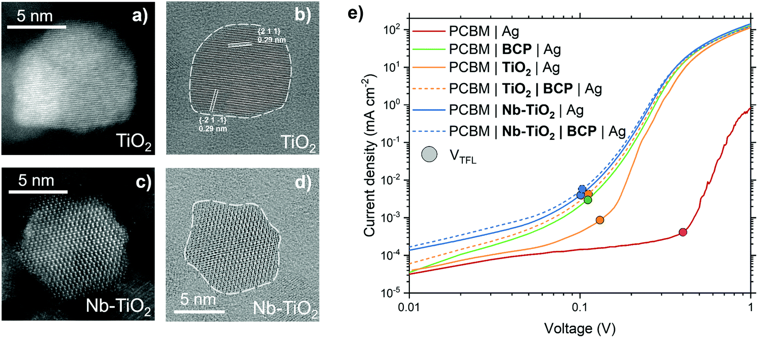 | ||
| Fig. 1 Light and dark-field TEM micrographs of pristine TiO2 (a and b) and Nb-TiO2 (c and d) nanoparticles. (e) Current–voltage curves for ‘electron only’ devices with different interfacial layers between PCBM–Ag contacts at logarithmic scale, measured in the dark. Solid circles indicate the trap-filled limit voltage (VTFL) for each configuration. The structure of the device is comprised as follows: ITO/SnO2/MAPbI3/PCBM/interfacial layer/Ag. | ||
Cathodic interfacial layers between PCBM and the metal electrode minimize the Schottky barrier that is often formed between a metal and a semiconductor, due to FLP, leading to a non-ohmic contact.42 This electrical barrier can be overcome by the introduction of very thin (<10 nm) layer between PCBM and metal, with metal oxides and organic small molecules being common choices aimed at reducing the defect and metal induced gap state density, between metal and semiconductor, which causes FLP.6 A simple and accessible method to probe the ohmic contact at this interface is to fabricate so-called ‘electron-only’ devices with different interfacial layers. Fig. 1e shows the current–voltage response for CH3NH3PbI3 (MAPbI3)-containing electron-only devices, measured in the dark, employing different PCBM-to-metal interlayers. With Ag in direct contact with PCBM, the electrical response is highly non-ohmic. A shallow slope in the ohmic region below 0.1 V, combined with a high trap-filled limit voltage (VTFL, the point at which the slope of the curve increases, indicated by a solid circle) is indicative of a Schottky barrier.43 With the addition of a layer of BCP,22,44,45 the ohmic response of the device is greatly improved, shown by the dramatically reduced VTFL. The increase in VTFL observed when using a TiO2 interlayer, compared to that of BCP, suggests the presence of trap-states within pristine TiO2. In the case of Nb-TiO2, a substantial improvement in this parameter is observed, suggesting that the addition of Nb both improves electron mobility and reduces the trap density within the metal oxide.37 While the addition of Nb reduces the resistance of this interlayer, we find the electrical properties of this interface can be further improved upon the addition of a layer of BCP, forming a Nb-TiO2/BCP bilayer. This bilayer yields a lower-resistance to electron transfer than either the Nb-TiO2 or BCP layers when used individually. The addition of BCP further reduces the slight Schottky barrier formed between Nb-TiO2 and metal electrode. This is the result of BCP's tendency to chelate with metals commonly used as electrodes such as silver, allowing a more intimate electronic contact between the Nb-TiO2 nanoparticles and the metal conductor. We propose that this bilayer reduces the FLP between ETL and metal, whilst offering enhanced carrier selectivity than BCP alone. The result is a bilayer which provides a highly versatile interface to couple semiconductors with metallic electrodes for high performance electronic and optoelectronic devices.
Interfacial bilayer simulation
To uncover the working mechanism of the Nb-TiO2/BCP bilayer we performed density functional theory (DFT) calculations. Fig. 2a shows simulated electronic density of states (DOS) plots for TiO2 with substitutional Nb atoms at Ti sites (1 in 8 Ti sites replaced with Nb, xNb = 0.125). The Fermi levels of all three TiO2 polymorphs (anatase, rutile and brookite, with brookite being the system of interest in this study) are shifted inside the conduction band of the material. This makes Nb-TiO2 somewhat metallic in nature, in agreement with previous studies.46,47 Even for the relatively high concentrations of Nb (xNb = 0.125), substitutional doping imparts minimal changes (around 1% or less) in the lattice parameter of brookite TiO2 (Fig. S2, ESI†). This is experimentally confirmed by the lack of lattice spacing differences between Nb-TiO2 and TiO2 observed in the TEM micrographs of Fig. 1a–d, where a much-reduced xNb of 0.05 is used. For brookite Nb-TiO2, we calculated the electrostatic potential for the (010) termination (Fig. 2b, other surfaces shown in Fig. S3 and S4, ESI†). From these simulations, we determined the work function of the (010) surface to be 3.94 eV. This shows that there is at least one surface of brookite Nb-TiO2 with a work function well-aligned with the lowest unoccupied molecular orbital (LUMO) of PCBM (3.9 eV) and less than the work function of the Ag electrode.16,48,49 This value also shows good agreement with our experimentally derived work function of 3.8 eV (Fig. S5, ESI†) and is consistent with the facile transfer of electrons from PCBM to Nb-TiO2.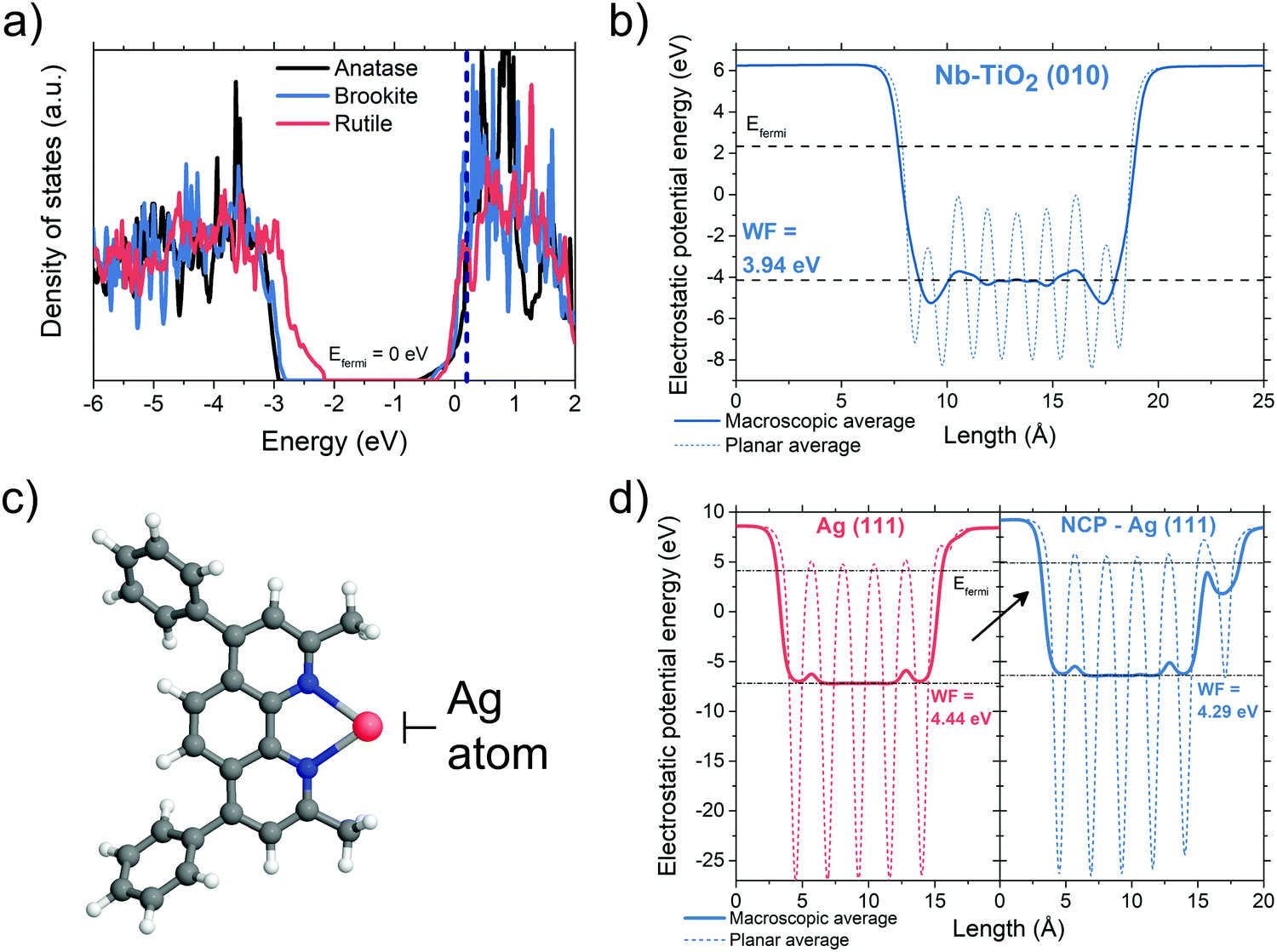 | ||
| Fig. 2 (a) Calculated electronic density of states for different TiO2 polymorphs doped with 12.5% Nb. (b) Calculated electrostatic potential energy for a (010) surface of brookite Nb0.125Ti0.875O2 showing a predicted work function of 3.94 eV. (c) Structure of bathocuproine (BCP) chelated with a silver atom. (d) Calculated electrostatic potential energies and work functions for a silver (111) surface (red trace) and the same silver surface with a layer of neocuproine (blue trace). | ||
Next, we probed the role of BCP in this interfacial structure. We found that BCP has a relatively low-lying HOMO energy around −6.07 eV (Fig. S6, ESI†). Moreover, we found that BCP molecules are able to chemically bond with Ag atoms (Fig. 2c) and hence suppress Ag diffusion towards the active layers of the device – which was previously found to be a cause of device degradation.50,51 This chelation effect is also well-known for the molecule neocuproine (NCP), which is an analogue of BCP containing identical metal-binding groups (shown in Fig. S7, ESI†) whilst being significantly faster to model.52 To explore the role of BCP–Ag interactions (equivalently, NCP–Ag interactions), we simulated the adsorption of NCP on an Ag (111) surface containing adatoms. The high adsorption energies in this system (Eb = 2.15 eV and 2.82 eV for pristine and adatom-containing surfaces respectively, Fig. S8, ESI†) indicate that NCP (and consequently BCP) molecules can efficiently functionalize the Ag surface. This decreases the work function of Ag-(111) by approximately 0.15 eV as shown in the electrostatic simulations of Fig. 2d (as well as Fig. S9 for other Ag surface configurations, ESI†), bringing it closer to the LUMO energy of PCBM and the work function of Nb-TiO2. To summarize the DFT-based results: (1) Nb-doped TiO2 is at least partially metallic, hence gap states are suppressed, (2) the addition of an additional BCP layer can block hole propagation and Ag diffusion, (3) the work functions of Nb-TiO2 and BCP-functionalized Ag surfaces are well-aligned with the LUMO level of PCBM, allowing a very low resistance ohmic contact between semiconductor and metal electrode.
Perovskite photovoltaic device performance
Fig. 3a shows a cross-section TEM micrograph of a perovskite solar cell used in this study in an ‘inverted’ p–i–n structure using a device stack containing NiOx HTL, MAPbI3 perovskite absorber, and PCBM ETL. We spin-coat a thin layer (<10 nm) of TiO2 or Nb-TiO2 nanoparticles to act as a CIL, as evidenced in the high magnification of Fig. 3b. Where appropriate, an additional ultra-thin layer of bathocuproine is employed between the metal oxide nanoparticles and electrode to further improve the ohmic contact. The resulting current–voltage (J–V) characteristics of the above “p–i–n” configuration MAPbI3 perovskite solar cells are present in Fig. 3c–e and summarized in Table 1. We note that device series resistance (Rs) is reduced upon the addition of BCP in the case of both pristine TiO2 (from 3.8 to 1.8 Ω cm−2) and Nb-TiO2 (from 3.5 to 1.1 Ω cm−2).53 This trend is in close agreement with the electron-only findings in Fig. 1e, and shows a substantial reduction in device series resistance as a result of the Nb-TiO2–BCP bilayer compared to BCP alone.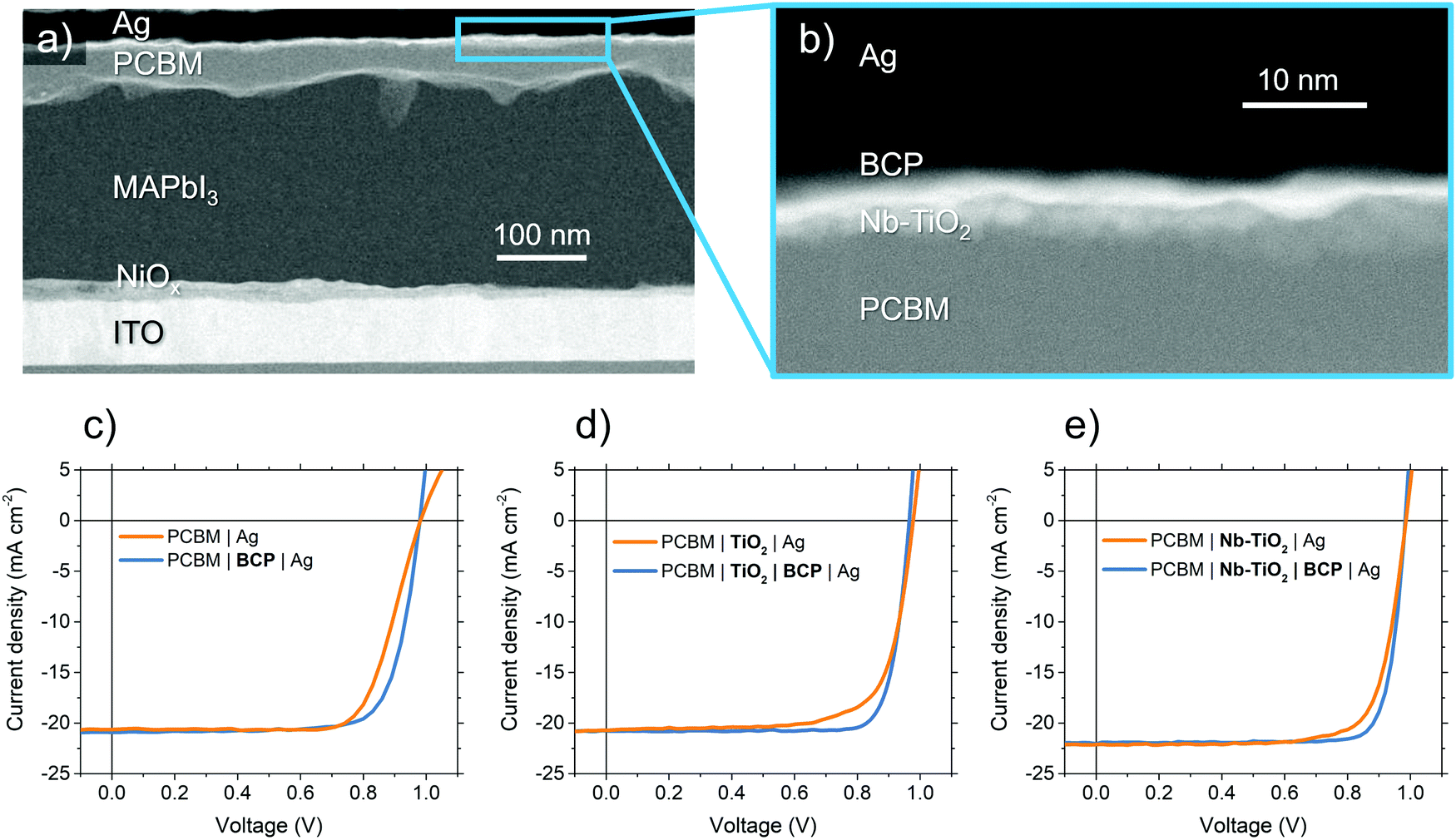 | ||
| Fig. 3 (a and b) Cross-sectional TEM micrographs of perovskite solar cells employing the Nb-TiO2 and BCP bilayer interfacial bilayer. (c–e) Current–voltage curves for perovskite solar cells employing different interfacial layers between PCBM charge selective layer and Ag electrode. Expanded J–V traces including information on hysteresis may be found in Fig. S10 (ESI†). | ||
| ITO|NiOx|MAPbI3| | J SC (mA cm−2) | V OC (V) | FF | PCE (%) | R S (Ω cm−2) |
|---|---|---|---|---|---|
| PCBM|Ag | 19.7 (20.6) | 0.96 (0.98) | 0.71 (0.73) | 13.5 (14.9) | (8.5) |
| PCBM|BCP|Ag | 20.1 (20.9) | 0.97 (0.98) | 0.77 (0.78) | 14.5 (15.8) | (3.1) |
| PCBM|TiO2|Ag | 20.4 (20.6) | 0.98 (1.00) | 0.74 (0.75) | 14.6 (15.2) | (3.8) |
| PCBM|TiO2|BCP|Ag | 20.7 (21.0) | 0.98 (1.00) | 0.79 (0.80) | 15.6 (16.1) | (1.8) |
| PCBM|Nb-TiO2|Ag | 21.5 (22.1) | 0.97 (0.98) | 0.76 (0.77) | 16.2 (16.7) | (3.5) |
| PCBM|Nb-TiO2|BCP|Ag | 21.8 (22.5) | 0.99 (1.00) | 0.82 (0.83) | 17.6 (18.5) | (1.1) |
Forward and reverse J–V scans can be seen in Fig. S10 (ESI†) and indicate a minimal degree of hysteresis. Statistical accounts of cell parameters are found in Fig. S11–S13 (ESI†) showing on-average differences in device performance. When BCP is introduced as the sole interfacial layer, as in Fig. 3c, the Schottky barrier is largely removed and the fill factor is increased from 0.73 to 0.78. While the use of a TiO2 interfacial layer yields results similar to that of BCP (Fig. 3d), the Nb-TiO2-containing device shows a substantial increase in JSC (from 20.6 to 22.1 mA cm−2, Fig. 3e). This increase in JSC and fill factor from pristine to Nb-doped TiO2 was also observed in an article by Chen and coworkers when employing Nb-TiO2 as an ETL in “n–i–p” perovskite solar cells.54 owing to a reduction in charge trapping within the metal oxide interlayer.
Fig. 4 illustrates this trapping using a transient photocurrent technique (TPC, Fig. 4a): with the pristine TiO2 device, a spike in transient photocurrent is observed. The same spike is absent in devices containing Nb-TiO2. This trapping effect is also observed in the solar cell external quantum efficiency (EQE, Fig. 4b) where devices with either a TiO2 interlayer or no interlayer exhibit a drop in response at longer wavelengths (>700 nm) compared to devices containing Nb-TiO2. Reduced EQE response in this region is correlated to increased recombination at the “rear” interface of the device, i.e. the perovskite/PCBM/interlayer interface. Since the perovskite/PCBM interface is unchanged in all cases, the role of Nb-doping in this system is therefore to both passivate TiO2 surface traps as well as to enhance the electron mobility of the nanoparticle film, reducing the barrier at the PCBM/Ag interface. Crucially, the addition of a secondary BCP layer greatly improves fill factor in devices with either a TiO2 (Fig. 3d) or Nb-TiO2 (Fig. 3e) interfacial layer, with the latter device exhibiting fill factors up to 0.83 in either J–V scan direction without negatively impacting other performance figures of merit. This significant fill factor is achieved both as a result of the reduction in trap density within the metal nanoparticle from Nb-doping, as well as BCP's work function modification of the Ag electrode, leading to a barrier-free interface. When measured over a range of illumination intensities, the fill factor response of TiO2 + BCP and Nb-TiO2 + BCP containing devices remains consistent between 0.80 and 0.84 (Fig. 4c). This is in comparison to a device containing no interlayer which shows a strong dependence on light intensity, suggesting a charge extraction limitation which is not present in the metal oxide-containing devices. A full account of current–voltage parameters as a function of light intensity may be found in Fig. S14 (ESI†). The solar cell fill factor values demonstrated here are among the highest currently reported for perovskite solar cells,55,56 indicating a highly ohmic contact between PCBM and silver electrode in interfacial bilayer devices, with particularly low contact resistance. Interestingly, an improvement in device performance is also observed when employing other commonly used electrode metals such as copper and gold in conjunction with Nb-TiO2 + BCP. Fig. S15 and Table S1 (ESI†) shows an increase in photocurrent density employing the bilayer in a device with a copper electrode, while gold electrode devices show an additional increase in fill factor (from 0.76 to 0.79) upon the addition of Nb-TiO2. Furthermore, the slope of the trap-filling region in electron-only devices is steeper for copper and gold electrodes when the interfacial bilayer is used (Fig. S15c and d, ESI†).
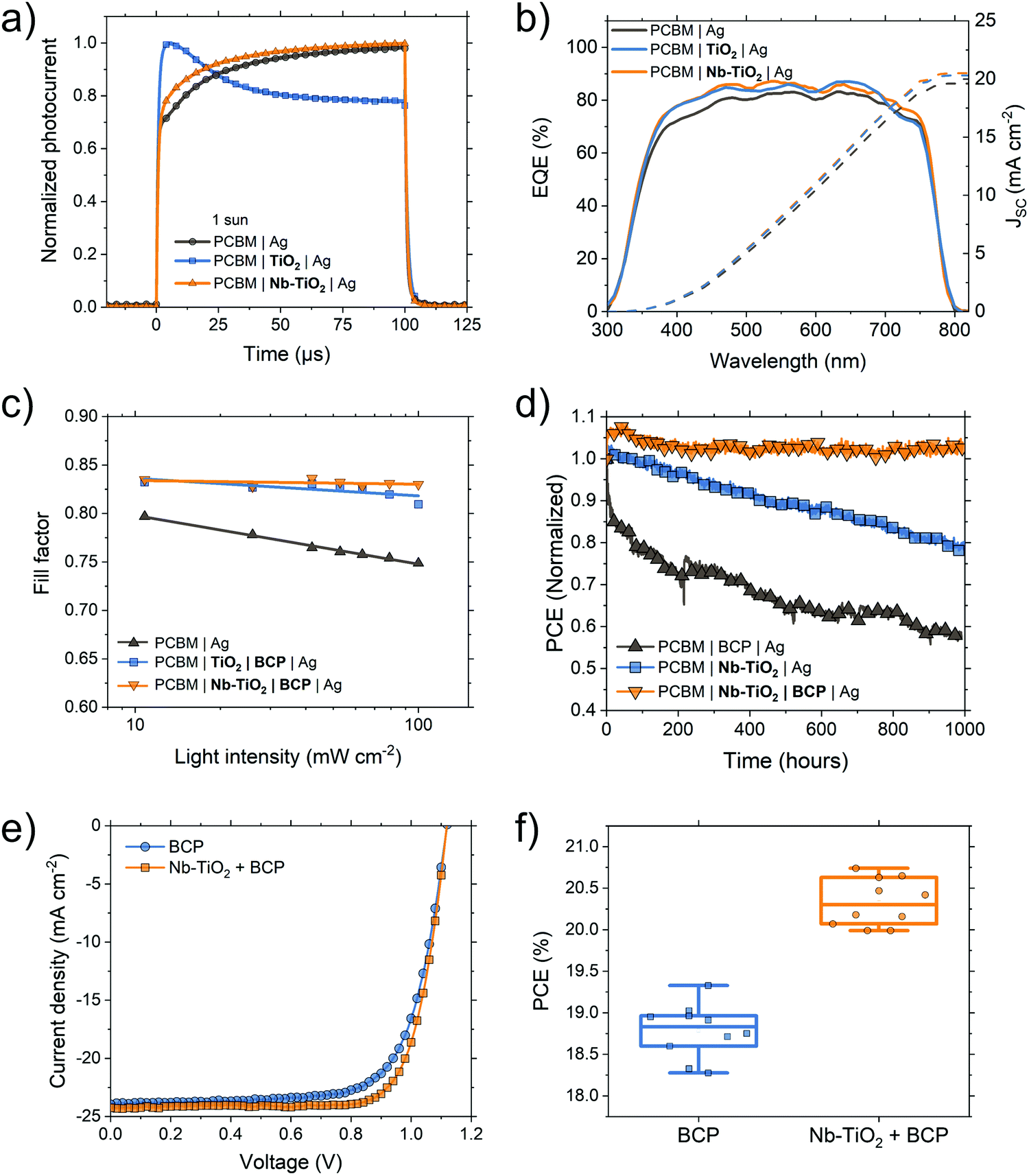 | ||
| Fig. 4 Transient photocurrent measurements (a), external quantum efficiency (b), and fill factor as a function of light intensity for different metal oxide nanoparticle interfacial layers (c). Also included is solar cell stability under a nitrogen atmosphere and 1 sun illumination (d). J–V curves from champion perovskite devices employing a PTAA HTL both with and without the interfacial bilayer (e). PCE statistics for PTAA HTL devices ((f), n = 10 for each interlayer). | ||
While NiOx HTLs have been proven to yield high fill factors in PSCs, polymers such as poly(triarylamine) (PTAA) and poly(4-butylphenyldiphenylamine) (poly-TPD) have emerged as more efficient alternatives given their high hole mobility and electron blocking properties.57–59 For MAPbI3 devices employing a PTAA HTL and Nb-TiO2/BCP cathodic bilayer, we demonstrate PCEs up to 20.7% in the “reverse” J–V scan direction, and 20.6% after 100 seconds held at maximum power voltage (Fig. 4e, f and Fig. S17, ESI†). This is compared to a BCP-only device with PCEs up to 19.3%. A full statistical account of these devices and their hysteresis may be found in Fig. S16 and S17 (ESI†). Further, to demonstrate that perovskite compositions beyond MAPbI3 may be used in this structure, we also fabricated devices using a multi-cation multi-anion perovskite composition [Cs0.05(FA0.83MA0.17)0.95PbI2.7Br0.3]. Corresponding J–V curves may be found in Fig. S18 (ESI†), with the bilayer containing device yielding 19.4% compared to 17.6% for a BCP-only device. It is worth noting that the 3 device structures (NiOx–MAPbI3, PTAA–MAPbI3, poly-TPD-Mixed cation & anion perovskite) demonstrated here were fabricated by different researchers on different days and, in the case of the latter, different universities: given the statistically significant performance improvement across a range of fabrication variables, we are confident of the proposed bilayer's efficacy in perovskite photovoltaics.
We find that perovskite solar cell operational stability is greatly improved upon the addition of this interfacial bilayer (Fig. 4d and Fig. S19, ESI†): under 1 sun continuous illumination (lamp spectrum presented in Fig. S20, ESI†) at open-circuit conditions in a nitrogen atmosphere maintained at 35 °C, MAPbI3 devices employing the Nb-TiO2/BCP bilayer retained their initial efficiency after 1000 hours. This is compared to devices containing only BCP which fall to 60% of their original efficiency during the same period. This decrease is primarily the result of a loss in fill factor and is attributed to metal electrode migration through the PCBM electron transport layer.60 The presence of a layer of metal oxide nanoparticles effectively blocks this migration, leading to the stabilization of the device's fill factor. The addition of an ultra-thin layer of silver-chealting BCP on top of this metal oxide layer further arrests metal migration over this test period, leading to highly stable perovskite solar cells under constant illumination.
Universality of Nb-TiO2|BCP layer in optoelectronic devices
The Nb-TiO2/BCP bilayer is applicable to electronic devices beyond perovskite solar cells. Here we extend this mechanism to other organic semiconductors such as those found in OPVs. In the OPV devices illustrated in Fig. 5a and 6d, an aluminum-coated calcium electrode is replaced with the Nb-TiO2/BCP bilayer and silver electrode. With no interfacial layer between organic active layer and silver, charge selectivity is reduced as demonstrated by the low VOC in Fig. 5a, by silver penetration into the organic active layer during thermal evaporation, as previously reported.61J–V parameters, statistics and EQE spectra for all devices listed in Table S2 and Fig. S21, S22 (ESI†), respectively. Upon the addition of a Nb-TiO2 interlayer between the bulk heterojunction and silver electrode, VOC is improved by over 70 mV due to the mechanical separation of metal and active layer – preventing silver penetration and subsequent de-rectification. However, the shortfall in VOC from the energetically-expected value indicates a barrier still present at the metal-oxide/metal interface. The combination of Nb-TiO2 and BCP at this interface leads to a further improvement in all photovoltaic parameters and an overall PCE of 12.6% – among the highest reported for this active layer combination. With the suppression of any Schottky barrier between active layer and electrode, the fill factor is improved from 0.63 to 0.72. The improvement in charge selectivity at this interface also improves VOC further to 0.72 V; comparable to the highest reported efficiency n–i–p structure devices, which typically exhibit higher overall performance.62,63 The use of this bilayer layer is, therefore, a useful component for efficient “p–i–n” OPV devices with high fill factors for simple binary blends, without the use of an easily-oxidized Ca/Al electrode.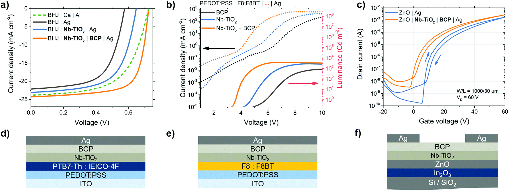 | ||
| Fig. 5 (a and d) Device structure and current–voltage curves for ‘normal’ p–i–n structure organic solar cell devices employing the metal oxide organic bilayer as an interface between semiconductor and metal electrode. (b and e) Device structure and current–luminance–voltage curves for organic LEDs employing various interfaces between semiconductor and metal electrode. (c and f) Device structure and current–voltage curves for inorganic thin-film transistors employing different semiconductor–metal interfaces. | ||
To further prove the applicability of this interface, Fig. 5e illustrates the structure of an OLED device containing a blend of poly(9,9-di-n-octylfluorenyl-2,7-diyl) (F8) and poly(9,9-dioctylfluorene-alt-benzothiadiazole) (F8BT) emitters followed by the Nb-TiO2 & BCP bilayer. Fig. 5b shows a current–voltage–luminance comparison between OLEDs employing combinations of the studied bilayer: when the Nb-TiO2/BCP bilayer is used, the emission turn-on voltage (dashed line) is reduced compared to a BCP-only device, resulting from the low barrier interlayer between emitter and metal electrode. This interface permits higher current injection at lower voltages, leading to an overall improvement in luminous efficiency (solid line): for this bilayer-containing OLED, peak luminous efficiency occurs at 4.3 V with 2.2 cd W−1 compared to the a BCP–Ag electrode device with a peak efficiency of 0.08 cd W−1 at 10.2 V (Fig. S23–S25, ESI†). This improvement in ohmic contact when using the Nb-TiO2/BCP bilayer is also applicable to thin film transistors (TFTs): Fig. 5f illustrates the schematic representation of such a transistor employing a silicon gate electrode and a semiconductor heterojunction of In2O3 and ZnO.64 In their standard configuration, metal source and drain electrodes directly contact the ZnO semiconductor. However, as demonstrated in Fig. 5c, the presence of the interfacial bilayer between ZnO and silver electrodes significantly reduces the transistor's threshold voltage (from 19.7 to 13.9 V – corresponding to a reduction of interfacial trap density of 1.3 × 1012 cm−2) and shifts the turn-on voltage closer to 0 V. A statistical account of TFT threshold voltages for all bilayer material combinations can be found in Fig. S26 (ESI†). The same performance improvement is observed in other TFT configurations such as those employing single-oxide semiconductors, and self-assembled monolayer (SAM)-functionalized metal gate electrodes (Fig. S27, ESI†). This reduction in turn-on voltage in simple TFTs is yet another indication that the electronic barrier between semiconductor and metal electrode is reduced as a result of the Nb-TiO2–BCP interlayer.
To conclude, we find that the addition of a solution processable bilayer of Nb-TiO2 nanoparticles in combination with a thin layer of organic BCP at the interface between semiconductor and metal electrode effectively reduces the Schottky barrier formed in a range of electronic device types and structures. We demonstrate that the versatility of this novel metal oxide–organic interface extends beyond perovskite and organic solar cells with other devices including OLEDs and TFTs exhibiting improvements in their figures of merit. The introduction of a low trap-density electron-selective metal oxide, Nb-TiO2, in contact with the device-side semiconductor facilitates efficient electron transfer. Meanwhile, the addition of BCP functionalizes the silver electrode's surface and brings its work function into more favorable energetic alignment with respect to many organic or inorganic semiconductors. The result of this bilayer is largely barrier-free electron injection from semiconductor into the external circuit, as well as dramatically improved operational stability in the case of perovskite solar cells. This new strategy paves the way for more efficient optoelectronic devices to be fabricated without an additional vacuum processing step, whilst opening a new avenue of research to find even more effective combinations of metal oxides and organic compounds to form into such a bilayer for high efficiency and stable optoelectronic devices.
Author contributions
J. T. and M. N. share equal contribution for conceiving the idea, designing the experiments and fabricating perovskite solar cells. M. N. fabricated and characterized OLEDs, N. G. performed electrical characterization of perovskite photovoltaics and aided in the design of experiments. L. T. performed the DFT calculations on Nb-TiO2 and BCP. M. F. O., B. H., M. R., and N. A. L. synthesized the metal oxide materials, A. S. performed electron microscopy, X. S. fabricated and characterized organic photovoltaics, E. Y. built the OLED characterization system. F. I. fabricated polymer HTL perovskite photovoltaics and antireflective coatings. Y.-H. L. and T. L. fabricated and characterized mixed cation perovskite photovoltaics, H. F. fabricated and characterized thin-film transistors, J. K. synthesized emitter materials for OLEDs. All co-authors discussed the paper and revised the manuscript. T. A., I. M. and D. B. supervised the work. J. T. wrote the manuscript.Conflicts of interest
D. B., N. G. and J. T. are co-founders of Iyris, L. L. C. H. J. S. is co-founder and Chief Scientific Officer of Oxford PV Ltd.Acknowledgements
L. T. acknowledges support for the computational time granted from GRNET in the National HPC facility – ARIS – under project STEM-2. D. B. acknowledges KAUST for financial support. Y.-H. L. and H. J. S. acknowledge the support from the UK Engineering and Physical Sciences Research Council (grant no. EP/M015254/2).References
- Y. Hou, X. Du, S. Scheiner, D. P. McMeekin, Z. Wang, N. Li, M. S. Killian, H. Chen, M. Richter, I. Levchuk, N. Schrenker, E. Spiecker, T. Stubhan, N. A. Luechinger, A. Hirsch, P. Schmuki, H. P. Steinrück, R. H. Fink, M. Halik, H. J. Snaith and C. J. Brabec, Science, 2017, 358, 1192–1197 CrossRef CAS PubMed.
- Y. Zhou, C. Fuentes-Hernandez, J. Shim, J. Meyer, A. J. Giordano, H. Li, P. Winget, T. Papadopoulos, H. Cheun, J. Kim, M. Fenoll, A. Dindar, W. Haske, E. Najafabadi, T. M. Khan, H. Sojoudi, S. Barlow, S. Graham, J. L. Brédas, S. R. Marder, A. Kahn and B. Kippelen, Science, 2012, 336, 327–332 CrossRef CAS PubMed.
- C. G. Tang, M. C. Y. Ang, K. K. Choo, V. Keerthi, J. K. Tan, M. N. Syafiqah, T. Kugler, J. H. Burroughes, R. Q. Png, L. L. Chua and P. K. H. Ho, Nature, 2016, 539, 536–540 CrossRef CAS PubMed.
- L. E. Black, B. W. H. van de Loo, B. Macco, J. Melskens, W. J. H. Berghuis and W. M. M. Kessels, Sol. Energy Mater. Sol. Cells, 2018, 188, 182–189 CrossRef CAS.
- C. Reichel, U. Würfel, K. Winkler, H. F. Schleiermacher, M. Kohlstädt, M. Unmüssig, C. A. Messmer, M. Hermle and S. W. Glunz, J. Appl. Phys., 2018, 123, 024505 CrossRef.
- M. Sajjad, X. Yang, P. Altermatt, N. Singh, U. Schwingenschlögl and S. De Wolf, Appl. Phys. Lett., 2019, 114, 071601 CrossRef.
- Z. Yin, J. Wei and Q. Zheng, Adv. Sci., 2016, 3 Search PubMed.
- T. H. Lai, S. W. Tsang, J. R. Manders, S. Chen and F. So, Mater. Today, 2013, 16, 424–432 CrossRef CAS.
- J. U. Lee, J. W. Jung, J. W. Jo and W. H. Jo, J. Mater. Chem., 2012, 22, 24265–24283 RSC.
- Z. Liu, M. Tian and N. Wang, J. Power Sources, 2014, 250, 105–109 CrossRef CAS.
- R.-Z. Liang, M. Babics, V. Savikhin, W. Zhang, V. M. Le Corre, S. Lopatin, Z. Kan, Y. Firdaus, S. Liu, I. McCulloch, M. F. Toney and P. M. Beaujuge, Adv. Energy Mater., 2018, 8, 1800264 CrossRef.
- X. Song, N. Gasparini, M. M. Nahid, S. H. K. Paleti, J. L. Wang, H. Ade and D. Baran, Joule, 2019, 3, 846–857 CrossRef CAS.
- W. Zhang, Y. Han, X. Zhu, Z. Fei, Y. Feng, N. D. Treat, H. Faber, N. Stingelin, I. McCulloch, T. D. Anthopoulos and M. Heeney, Adv. Mater., 2016, 28, 3922–3927 CrossRef CAS PubMed.
- J. Smith, R. Hamilton, Y. Qi, A. Kahn, D. D. C. Bradley, M. Heeney, I. McCulloch and T. D. Anthopoulos, Adv. Funct. Mater., 2010, 20, 2330–2337 CrossRef CAS.
- Z. A. Lamport, K. J. Barth, H. Lee, E. Gann, S. Engmann, H. Chen, M. Guthold, I. McCulloch, J. E. Anthony, L. J. Richter, D. M. DeLongchamp and O. D. Jurchescu, Nat. Commun., 2018, 9, 5130 CrossRef PubMed.
- O. Malinkiewicz, A. Yella, Y. H. Lee, G. M. Espallargas, M. Graetzel, M. K. Nazeeruddin and H. J. Bolink, Nat. Photonics, 2014, 8, 128–132 CrossRef CAS.
- L. Meng, J. You, T. F. Guo and Y. Yang, Acc. Chem. Res., 2016, 49, 155–165 CrossRef CAS PubMed.
- D. Luo, W. Yang, Z. Wang, A. Sadhanala, Q. Hu, R. Su, R. Shivanna, G. F. Trindade, J. F. Watts, Z. Xu, T. Liu, K. Chen, F. Ye, P. Wu, L. Zhao, J. Wu, Y. Tu, Y. Zhang, X. Yang, W. Zhang, R. H. Friend, Q. Gong, H. J. Snaith and R. Zhu, Science, 2018, 360, 1442–1446 CrossRef CAS PubMed.
- X. Zheng, J. Troughton, N. Gasparini, Y. Lin, M. Wei, Y. Hou, J. Liu, K. Song, Z. Chen, C. Yang, B. Turedi, A. Y. Alsalloum, J. Pan, J. Chen, A. A. Zhumekenov, T. D. Anthopoulos, Y. Han, D. Baran, O. F. Mohammed, E. H. Sargent and O. M. Bakr, Joule, 2019, 3, 1–14 CrossRef.
- H. Li, D. He, Q. Zhou, P. Mao, J. Cao, L. Ding and J. Wang, Sci. Rep., 2017, 7, 40134 CrossRef CAS PubMed.
- L. Chen, G. Wang, L. Niu, Y. Yao, Y. Guan, Y. Cui and Q. Song, RSC Adv., 2018, 8, 15961–15966 RSC.
- C. Chen, S. Zhang, S. Wu, W. Zhang, H. Zhu, Z. Xiong, Y. Zhang and W. Chen, RSC Adv., 2017, 7, 35819–35826 RSC.
- A. Savva, I. Burgués-Ceballos and S. A. Choulis, Adv. Energy Mater., 2016, 6, 1–8 CrossRef.
- S. Bai, Z. Wu, X. Wu, Y. Jin, N. Zhao, Z. Chen, Q. Mei, X. Wang, Z. Ye, T. Song, R. Liu, S. tong Lee and B. Sun, Nano Res., 2014, 7, 1749–1758 CrossRef CAS.
- Z. Zhu, Y. Bai, X. Liu, C.-C. Chueh, S. Yang and A. K.-Y. Jen, Adv. Mater., 2016, 28, 6478–6484 CrossRef CAS PubMed.
- P. Docampo, J. M. Ball, M. Darwich, G. E. Eperon and H. J. Snaith, Nat. Commun., 2013, 4, 2761 CrossRef PubMed.
- D. X. Yuan, X. D. Yuan, Q. Y. Xu, M. F. Xu, X. B. Shi, Z. K. Wang and L. S. Liao, Phys. Chem. Chem. Phys., 2015, 17, 26653–26658 RSC.
- J. Troughton, N. Gasparini and D. Baran, J. Mater. Chem. A, 2018, 6, 21913–21917 RSC.
- W. Chen, L. Xu, X. Feng, J. Jie and Z. He, Adv. Mater., 2017, 29, 1603923 CrossRef PubMed.
- M. Neophytou, M. De Bastiani, N. Gasparini, E. Aydin, E. Ugur, A. Seitkhan, F. Moruzzi, Y. Choaie, A. J. Ramadan, J. R. Troughton, R. Hallani, A. Savva, L. Tsetseris, S. Inal, D. Baran, T. D. Anthopoulos, H. J. Snaith, S. De Wolf and I. Mcculloch, ACS Appl. Energy Mater., 2019, 2, 8090–8097 CrossRef CAS.
- J. Saito, T. Oku, A. Suzuki and T. Akiyama, AIP Conf. Proc., 2016, 1709, 2–9 Search PubMed.
- B.-X. Chen, H.-S. Rao, W.-G. Li, Y.-F. Xu, H.-Y. Chen, D.-B. Kuang and C.-Y. Su, J. Mater. Chem. A, 2016, 4, 5647–5653 RSC.
- Y. Lv, B. Cai, Q. Ma, Z. Wang, J. Liu and W.-H. Zhang, RSC Adv., 2018, 8, 20982–20989 RSC.
- G. Xiao, C. Shi, K. Lv, C. Ying and Y. Wang, ACS Appl. Energy Mater., 2018, 1, 2576–2581 CrossRef CAS.
- Y. Lv, B. Cai, Q. Ma, Z. Wang, J. Liu and W.-H. Zhang, RSC Adv., 2018, 8, 20982–20989 RSC.
- P. Cheng and X. Zhan, Chem. Soc. Rev., 2016, 45, 2544–2582 RSC.
- W. Chen, Y. Wu, Y. Yue, J. Liu, W. Zhang, X. Yang, H. Chen, E. Bi, I. Ashraful, M. Grätzel and L. Han, Science, 2015, 350, 944–948 CrossRef CAS PubMed.
- X. Lü, X. Mou, J. Wu, D. Zhang, L. Zhang, F. Huang, F. Xu and S. Huang, Adv. Funct. Mater., 2010, 20, 509–515 CrossRef.
- L. Kong, C. Wang, H. Zheng, X. Zhang and Y. Liu, J. Phys. Chem. C, 2015, 119, 16623–16632 CrossRef CAS.
- P. Hasin, M. A. Alpuche-Aviles, Y. Li and Y. Wu, J. Phys. Chem. C, 2009, 113, 7456–7460 CrossRef CAS.
- M. Fehse, S. Cavaliere, P. E. Lippens, I. Savych, A. Iadecola, L. Monconduit, D. J. Jones, J. Rozière, F. Fischer, C. Tessier and L. Stievano, J. Phys. Chem. C, 2013, 117, 13827–13835 CrossRef CAS.
- B. Xiao, H. Wu and Y. Cao, Mater. Today, 2015, 18, 385–394 CrossRef CAS.
- X. Wu, H. Li, K. Wang, X. Sun and L. Wang, RSC Adv., 2018, 8, 11095–11101 RSC.
- J. Troughton, K. Hooper and T. M. Watson, Nano Energy, 2017, 39, 60–68 CrossRef CAS.
- D.-X. Yuan, X.-D. Yuan, Q.-Y. Xu, M.-F. Xu, X.-B. Shi, Z.-K. Wang and L.-S. Liao, Phys. Chem. Chem. Phys., 2015, 17, 26653–26658 RSC.
- X. D. Liu, E. Y. Jiang, Z. Q. Li and Q. G. Song, Appl. Phys. Lett., 2008, 92, 252104 CrossRef.
- J. Osorio-Guillén, S. Lany and A. Zunger, Phys. Rev. Lett., 2008, 100, 036601 CrossRef PubMed.
- J. Seo, S. Park, Y. Chan Kim, N. J. Jeon, J. H. Noh, S. C. Yoon and S. Il Seok, Energy Environ. Sci., 2014, 7, 2642–2646 RSC.
- M. Chelvayohan and C. H. B. Mee, J. Phys. C: Solid State Phys., 1982, 15, 2305–2312 CrossRef CAS.
- H. Yoshida, J. Phys. Chem. C, 2015, 119, 24459–24464 CrossRef CAS.
- J. Li, Q. Dong, N. Li and L. Wang, Adv. Energy Mater., 2017, 7, 1602922 CrossRef.
- E. V. Solovyeva, A. Rakhimbekova, Y. V. Lanchuk, L. A. Myund and A. S. Denisova, J. Raman Spectrosc., 2018, 49, 207–214 CrossRef CAS.
- A. G. Aberle, S. R. Wenham and M. A. Green, Conference Record of the IEEE Photovoltaic Specialists Conference, IEEE, 1993, vol. 1, pp. 133–139 Search PubMed.
- B. X. Chen, H. S. Rao, W. G. Li, Y. F. Xu, H. Y. Chen, D. Bin Kuang and C. Y. Su, J. Mater. Chem. A, 2016, 4, 5647–5653 RSC.
- M. Stolterfoht, C. M. Wolff, Y. Amir, A. Paulke, L. Perdigó N-Toro, P. Caprioglio and D. Neher, Energy Environ. Sci., 2017, 10, 1530 RSC.
- E. Aydin, M. De Bastiani and S. De Wolf, Adv. Mater., 2019, 31, 1900428 CrossRef PubMed.
- J. Sun, J. Lu, B. Li, L. Jiang, A. S. R. Chesman, A. D. Scully, T. R. Gengenbach, Y. B. Cheng and J. J. Jasieniak, Nano Energy, 2018, 49, 163–171 CrossRef CAS.
- M. Stolterfoht, C. M. Wolff, Y. Amir, A. Paulke, L. Perdigón-Toro, P. Caprioglio and D. Neher, Energy Environ. Sci., 2017, 10, 1530–1539 RSC.
- M. Saliba, J. P. Correa-Baena, C. M. Wolff, M. Stolterfoht, N. Phung, S. Albrecht, D. Neher and A. Abate, Chem. Mater., 2018, 30, 4193–4201 CrossRef CAS.
- K. Domanski, J. P. Correa-Baena, N. Mine, M. K. Nazeeruddin, A. Abate, M. Saliba, W. Tress, A. Hagfeldt and M. Grätzel, ACS Nano, 2016, 10, 6306–6314 CrossRef CAS PubMed.
- G. Zhang, S. A. Hawks, C. Ngo, L. T. Schelhas, D. T. Scholes, H. Kang, J. C. Aguirre, S. H. Tolbert and B. J. Schwartz, ACS Appl. Mater. Interfaces, 2015, 45, 25247–25258 CrossRef PubMed.
- X. Song, N. Gasparini, L. Ye, H. Yao, J. Hou, H. Ade and D. Baran, ACS Energy Lett., 2018, 3, 669–676 CrossRef CAS.
- J. Wang, S. Xie, D. Zhang, R. Wang, Z. Zheng, H. Zhou and Y. Zhang, J. Mater. Chem. A, 2018, 6, 19934–19940 RSC.
- Y. H. Lin, H. Faber, J. G. Labram, E. Stratakis, L. Sygellou, E. Kymakis, N. A. Hastas, R. Li, K. Zhao, A. Amassian, N. D. Treat, M. McLachlan and T. D. Anthopoulos, Adv. Sci., 2015, 2, 1–12 Search PubMed.
Footnote |
| † Electronic supplementary information (ESI) available. See DOI: 10.1039/c9ee02202c |
| This journal is © The Royal Society of Chemistry 2020 |