DOI:
10.1039/D0DT02174A
(Paper)
Dalton Trans., 2020,
49, 13786-13796
Electrochemical deposition of a semiconducting gold dithiolene complex with NIR absorption†
Received
18th June 2020
, Accepted 24th September 2020
First published on 24th September 2020
Abstract
Here, the synthesis of a new anionic gold dithiolene complex, NBu4·[1-i], and that of its corresponding neutral gold complex 2 is reported. Complex 2 shows strong absorption into the IR, semiconductivity (σRT = 3.06 × 10⁻⁷ S cm−1) with an activation energy of 0.25 eV, and weakly temperature dependent paramagnetic susceptibility, indicating strong intermolecular interactions in the solid state. As a consequence of their strong intermolecular interactions, neutral gold dithiolene complexes are often highly insoluble, limiting their utility and processability. Electrochemical deposition is used to deposit conductive films of complex 2, which retain the NIR properties present in the bulk material, indicting that the strong intermolecular interactions are retained in the film.
Introduction
Metal bis-1,2-dithiolene complexes have been widely studied over the last 60 years due to their diverse optical, electronic and magnetic properties, which can be tuned through modification of the dithiolene ligands or variation of the metal centre.1,2 Many neutral metal dithiolenes exhibit strong absorptions into the near infrared region (NIR), allowing use in photodetectors,3 and non-linear optics applications,3,4 while gold and nickel dithiolene complexes in particular have been studied for their conductive properties, ranging from semiconductors for field-effect transistors (FETs),5–7 to molecular metals,8–15 and superconductors.16,17 An attractive feature of neutral dithiolene complexes is their square planar geometry and delocalized electronic structure which can give rise to strong intermolecular interactions, a requirement for appreciable solid state conductivity. However, these strong intermolecular interactions typically result in the dithiolene complexes having extremely low solubility and volatility, which inhibits their ability to be processed and incorporated into devices. Electrodeposition has been used to deposit thin films of molecular conductors on conductive substates,18,19 and we have previously harnessed the technique to grow films of highly insoluble molecules, including nickel dithiolenes, via the electrochemical oxidation of a more soluble anionic precursor.20–23 However, to our knowledge this approach has not been applied to neutral gold dithiolenes. Accordingly, this work represents the first study where the technologically-attractive properties of neutral gold dithiolene complexes have been realized in thin film form.
In this work we present the synthesis of a new anionic gold dithiolene complex NBu4·[1-i] and subsequently the neutral complex 2via chemical oxidation, and study of its magnetic, optical and electronic properties, including conductivity under pressure. Thin films of 2 were then deposited via electrodeposition onto conductive indium–tin oxide (ITO) substrates from solutions of NBu4·[1-i] under potentiostatic conditions, and the optical properties and surface morphology was investigated.
Results and discussion
Synthesis
The anionic precursor NBu4·[1] was synthesized via the deprotection of the dithiolone, 4-(4-chlorophenyl)-1,3-dithiol-2-one, with sodium methoxide followed by addition of KAuCl4 (Scheme 1). As the dithiolone is asymmetric, the salt was initially obtained as a mixture of the cis and trans isomers, distinguishable by a small (0.01 ppm) difference between the dithiolene protons in the 1H NMR. As reported for other gold dithiolene complexes,8,24,25–32,33–37 the two isomers do not appear to interconvert in solution, and thus a pure isomer NBu4·[1-i] (NMR in Fig. S1†) was isolated via selective precipitation/crystallization in reasonable yield (40%). As single crystals of NBu4·[1-i] were not obtained, it was not possible to determine whether this was the cis or trans isomer. The neutral radical complex 2 was then synthesised via oxidation with I2 and collected by filtration to give an almost completely insoluble and poorly crystalline (Fig. S2†) powder. Attempts were made to isolate single crystals of 2 by electrocrystallisation, which produced thin green-black needles, however all samples were poorly diffracting.
 |
| | Scheme 1 Synthesis of neutral radical 2. | |
Electronic absorption spectroscopy
The absorption spectra (Fig. 1 and Table 1) of NBu4·[1-i] and 2 were recorded in acetonitrile and chloroform, respectively. In the case of 2 the solubility was too low to accurately determine extinction coefficients. Intense bands (ε > 2 × 10⁴ M−1 cm−1) in the region <300 nm can be assigned to π → π* transitions on the ligand framework for both NBu4·[1-i] and 2. At lower energies weakly absorbing transitions (ε < 500 M−1 cm−1) can be observed for NBu4·[1-i], that can be broadly assigned to d–d transitions with some additional ligand contribution. In the case of 2, an intense transition is observed at 1425 nm, characteristic of neutral gold dithiolene complexes and has previously been assigned to a SOMO−1 to SOMO transition.28,36–38
 |
| | Fig. 1 UV-vis-NIR absorption spectrum of NBu4·[1-i] in acetonitrile and 2 in chloroform. Inset highlights the weak transitions. | |
Table 1 Data of the electronic spectra of NBu4·[1-i] and 2 in CH2Cl2 solution
| Compound |
λ
max/nm (ε/M−1 cm−1) |
|
NBu4·[1-i]
|
251.5 (31![[thin space (1/6-em)]](https://www.rsc.org/images/entities/char_2009.gif) 102), 270 (28109), 293 (24013), 355 (9322), 474 (187), 754 (81) 102), 270 (28109), 293 (24013), 355 (9322), 474 (187), 754 (81) |
|
2
|
277, 429, 556, 585, 687, 1425 |
Infrared spectroscopy
Fourier transform infra-red (FTIR) spectroscopy was performed on NBu4·[1-i], 2 and the ligand precursor, 4-(4-chlorophenyl)-1,3-dithiol-2-one (Fig. 2). There is reasonable overlap between the fingerprint regions for all 3 compounds, with some key differences. In all three spectra, peaks relating to C–Cl stretches and aromatic in-plane C–H bending can be seen at 1091 cm−1 and 1008 cm−1. The aromatic C–H stretching frequencies can also be found in the 900–700 cm−1 region. The ligand precursor has a peak at 1630 cm−1 associated with the carbonyl of the dithiol-2-one, while a strong signal from the tetrabutylammonium cation can be seen in the 3000–2800 cm−1 region for NBu4·[1-i]. The alkene C![[double bond, length as m-dash]](https://www.rsc.org/images/entities/char_e001.gif) C stretches can be seen between 1600–1500 cm−1 for both the ligand precursor and NBu4·[1-i], while they shift to a lower frequency for 2. This is coupled with an increase in intensity of the peak at 1205 cm−1, which is visible in the spectra for NBu4·[1-i] and 2, though it is more pronounced for 2. This peak is related to the CS stretch and its increase in intensity upon oxidation could indicate an increase in dithioketone-like character upon oxidation, something that has previously been observed through changes in the C–S bond length from single crystal diffraction data.28 The most significant difference in the spectra is the presence of a significant absorption tailing into the high energy region of the spectrum for 2. This absorption is likely due to the onset of electronic transitions, suggesting that 2 is a semiconductor with a relatively narrow bandgap in the solid state.
C stretches can be seen between 1600–1500 cm−1 for both the ligand precursor and NBu4·[1-i], while they shift to a lower frequency for 2. This is coupled with an increase in intensity of the peak at 1205 cm−1, which is visible in the spectra for NBu4·[1-i] and 2, though it is more pronounced for 2. This peak is related to the CS stretch and its increase in intensity upon oxidation could indicate an increase in dithioketone-like character upon oxidation, something that has previously been observed through changes in the C–S bond length from single crystal diffraction data.28 The most significant difference in the spectra is the presence of a significant absorption tailing into the high energy region of the spectrum for 2. This absorption is likely due to the onset of electronic transitions, suggesting that 2 is a semiconductor with a relatively narrow bandgap in the solid state.
 |
| | Fig. 2 Infrared spectrum of the ligand precursor, NBu4·[1-i] and 2. | |
Cyclic voltammetry
The electrochemical properties of NBu4·[1-i] were investigated by cyclic voltammetry (Fig. 3 Left, Table 2). A full scan of the potential window (−1.5–2.0 V vs. Fc/Fc+) revealed 3 irreversible oxidations, corresponding to the E1−/0, E0/1+ and possibly E1+/2+ processes or oxidation of a daughter product. There is also one irreversible reduction, corresponding to the E2−/1− process. The electrochemical HOMO–LUMO gap was estimated from the difference in the onset of the first oxidation and reduction peaks, and agrees reasonably well with the energy of the d–d transition calculated from the absorption spectrum of NBu4·[1-i]. The first oxidation and reduction peaks show a strong similarity with structurally related gold dithiolene complexes.28,39,40
 |
| | Fig. 3 Left: Cyclic voltammogram at 0.1 V s−1 of NBu4·[1-i] at RT in acetonitrile with 0.1 M [TBA][PF6] as the supporting electrolyte. Right: Cyclic voltammogram of 10 successive scans at 0.10 V s−1 of NBu4·[1-i] at RT in acetonitrile with 0.1 M [TBA][PF6] as the supporting electrolyte. | |
Table 2 Electrochemical data for NBu4·[1-i]
| |
E
−2/−1 (V) |
E
−1/0 (V) |
E
0/+1 (V) |
E
+1/+2 (V) |
HOMO–LUMO gapa (eV) |
|
Electrochemical HOMO–LUMO gap calculated as the difference between the onset of the first oxidation and reduction waves.
|
|
NBu4·[1-i]
|
−1.9 |
0.04 |
0.91 |
1.05 |
1.74 |
During the electrochemical studies, it was observed that dark green films were depositing on the working electrode. As neutral gold dithiolene complexes are known to be insoluble it was assumed that this deposition occurred during the first oxidation; as a result the first oxidation process was then studied in further detail. Successive scans were performed between −0.5 V and 0.3 V (Fig. 3, right) in order to prevent interference from subsequent redox processes. The first thing of note is that in contrast to the full scan, a cathodic peak appears on the reversal of the scan direction, indicating that the previously observed irreversibility of the E−1/0 redox potential was due to chemical irreversibility of the E0/+1 and/or the E+1/+2 redox couple. Secondly, during the first oxidative scan the current increases abruptly, attributed to an overpotential associated with nucleation, while on subsequent scans a tend towards a normal exponential current occurs, suggesting that the neutral radical is not completely reduced and removed from the surface upon the backward scan. This is further corroborated by Ipa > Ipc and the area of the anodic scan being larger than the cathodic scan for each cycle. Variation in scan rate (Fig. S3†) revealed that while peak currents vary linearly with the square root of the scan rate the anodic peak current is consistently larger than the cathodic peak current, and the cathodic peak shifts with scan rate, suggesting that the first oxidation is chemically reversible but electrochemically irreversible.41,42
Magnetic properties
The temperature dependence (Fig. 4) of the magnetic susceptibility of 2 was measured using a SQUID magnetometer in the range 3–300 K, and corrected for sample diamagnetism. The susceptibility of 2 is far lower than expected for isolated S = 1/2 molecules, 2.0 × 10⁻⁴ emu mol−1 at room temperature, and is almost temperature independent from 300 to 60 K. The rapid increase approaching 0 K is attributed to 2% paramagnetic defects. Similar behaviour has been observed for other gold dithiolene complexes, and has been attributed to strong electron correlation.9,24,26–29,43
 |
| | Fig. 4 Magnetic Susceptibility of chemically oxidised 2. | |
Conductive properties
Ambient.
The temperature dependence of the conductivity of 2 was investigated on a compressed pellet in the 190–300 K range. The conductivity of 2 at room temperature is 3.06 × 10⁻⁷ S cm−1, a value comparable with that previously reported for compressed pellets of gold dithiolenes.44–46 Upon cooling, semiconductor behaviour was observed with an activation energy of 0.25 eV (Fig. 5, left). This small activation energy is consistent with the observation of a low energy absorption that extends into the infrared, and is similar to energy gaps reported for other gold dithiolene complexes.25,27,28,47
 |
| | Fig. 5 Left: Temperature dependence of the conductivity for 2 in the temperature range of 190–300 K on a compressed pellet. The blue line indicates the theoretical fit with an activation energy of 0.25 eV. Right: Pressure dependent conductivity of a compressed pellet of 2. A linear plot of pressure vs. conductivity is available in the ESI.† | |
Pressure dependence.
Several gold dithiolene complexes have been reported to show enhanced conductivity, even superconductivity, under the application of pressure.24,25,29,47–50 With this in mind, the effect of pressure on the conductivity of 2 was investigated through measurements on a compressed pellet. As shown in Fig. 5, the conductivity of the amorphous pressed pellet of 2 increases exponentially with applied pressure, up to a factor of 49 upon application of 2 GPa. Exponential increases in conductivity with applied pressure have previously been observed for other neutral gold complexes, such as [Au(Et-thiazdt)2] and [Au(iPr-thiazdt)2], single crystals of which showed an exponential increase in conductivity up to 1.3 and 1.5 GPa, respectively, equating to increases by a factor of 1000 and 40, respectively.24,29 At higher pressures, the conductivity of both complexes showed a linear dependence on pressure; this transition was attributed to the switchover from semiconductor to metallic behaviour. In the case of 2, this suggests that the conductive behaviour remains in the semiconductor regime below 2.0 GPa. Increases in conductivity on the order of 10–1000 fold have been reported for single crystals of gold dithiolene complexes in this pressure range.25,29,47,49,50 It is noted that despite this increase under pressure, the conductivity of 2 is low, reaching 6.3 × 10⁻⁶ S cm−1 at 2 GPa, this could be due to unfavourable packing interactions, or dimerization within the structure. We note also that the low conductivity and semiconductor behaviour is consistent with a lack of inclusion of any counterion dopant.
Computational studies
To gain further insight into the electronic properties of 2 (TD-)DFT calculations were performed on the cis and trans isomers to identify the character of the frontier orbitals and the nature of the electronic transitions. The structures of the anionic complexes, [trans-1]− and [cis-1]−, and the neutral radicals trans-2 and cis-2 were optimised; small differences were observed between the anionic and neutral structures in terms of the calculated Au–S bond length and dihedral angle between the dithiolene and phenyl rings (32.9° for [trans-1]−, −38.1° for trans-2, 32.8° for [cis-1]−, −38.4° for cis-2). The frontier molecular orbitals and energies of trans-2 are shown in Fig. 6, while the frontier orbitals for cis-2 are found in Fig. S8.† It can be seen that for both isomers the frontier orbitals all feature significant contributions from the dithiolene ligand; the αSOMO−1 and βSOMO are delocalised over the whole of the ligand including the phenyl rings, while the αSOMO, αLUMO and βLUMO are mostly localised over the dithiolene ring and the gold centre. The contribution from the gold centre to the αSOMO is relatively small, 3% for both trans-2 and cis-2 (see Tables S1 and 2†); indicating that the majority of the spin density is located across the ligand framework. As a result of this significant ligand contribution, intermolecular interactions in the solid state will promote strong molecular interactions; this has been seen in other gold dithiolene complexes.28,29,40,51 TD-DFT calculations were performed to investigate the nature of low energy optical transitions, and the results are shown in Fig. 7 (Tables S3 and 4†). Although the transition energies are slightly underestimated, the simulated absorption spectra show good agreement with the experimental data. In particular, the intense NIR absorption of 2 at 1425 nm can be assigned to the β SOMO−1 to SOMO transition, while other low energy absorptions in the spectra for 2 can be assigned to transitions from the SOMO−1 to LUMO.
 |
| | Fig. 6 Frontier molecular orbitals of 2 (isocontour set at 0.02000). | |
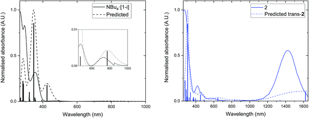 |
| | Fig. 7 Simulated and experimental UV/Vis/NIR spectra of Left: NBu4·[1-i] and [trans-1]− and Right: trans-2 and 2 based on TD-DFT calculations. The predicted spectrum is shown in dashed lines, and the experimental spectra in solid lines. | |
Overall, the calculated electronic structure of 2 agrees well with previously reported studies on gold dithiolene complexes.28,36,38,52,53
Electrodeposition of thin films
Electrodeposition was investigated as a method for growing thin films of 2. Films were deposited onto FTO (fluorine-doped tin oxide) from a 1 mM solution of NBu4·[1-i] in a 0.1 M [TBA][PF6] DMF electrolyte. The films were deposited under potentiostatic conditions with a potential of 0.29 V vs. Fc/Fc+ in order to avoid over-oxidation, as the cyclic voltammetry suggested that the 2nd/3rd oxidation of NBu4·[1-i] results in a chemically irreversible transformation. The deposition time was varied from 10 to 40 min (films 1–3). In order to investigate the impact of substrate choice, a film was also deposited on FTO coated with a thin layer of platinum (film 4).
For all the films the cumulative charge per cm2 increases steadily over the deposition times (Fig. 8), suggesting that the film formed is conductive. The initial current is very large (>1.5 mA) for all films, and then decreases rapidly before reaching a steady current of approximately 0.1 mA for films 1–3, and 0.05 mA for film 4 (Fig. 9). The large initial current is due to the formation of the double layer and initial absorption of dithiolene anions at the surface of the substrate; the large drop in current is then due to the local depletion of the NBu4·[1-i] salt near the FTO electrode's surface. The slow decrease in the current after the initial 50 seconds of deposition indicated the formation of the film is now diffusion dependent. A more detailed examination of the kinetics of the deposition process can be gleaned from a plot of the charge per cm2 against the t1/2 (Fig. 8). Here, a linear regime, which begins at approximately 10 s1/2, is observed for all films. Extrapolation from this linear region results in a negative y-intercept, suggesting a diffusion controlled reaction in the latter stages of the deposition, while in the earlier stages of the reaction the process is under mixed control.
 |
| | Fig. 8 Total charge per cm2 against t1/2 for the deposition of films 1–4. | |
 |
| | Fig. 9 Current response of films 1–4 during potentiostatic growth at 0.29 V vs. Fc+/Fc. Inset: Estimated surface coverage. | |
The film surface coverage was estimated by measuring the area of the deposited film and integrating the current signal over the deposition time (Fig. 9, inset). In the case of the FTO films (1–3) increasing the deposition time resulted in an increase in surface coverage, with a deposition rate range of 3.3–4.2 × 10⁻⁸ mol min−1 for all three films. In the case of the film deposited on Pt-coated FTO (film 4) the surface coverage was low despite a reasonably lengthy deposition time, suggesting different growth conditions on a different electrode surface.
Electronic absorption of thin films
The electronic absorption of the films was measured by diffuse reflectance spectroscopy (Fig. 10). The films show strong absorptions in the 300–500 nm range and weaker absorptions in the 500–700 nm range, comparable to those observed in solution for 2, which correspond to the π → π* and d–d based transitions. In the 1000–1800 nm range strong absorptions can be seen for all of the films and, in the case of films 3 and 4 multiple peaks are observed. Based on the solution absorption spectra of 2 these peaks likely originate from the SOMO−1 to SOMO transitions, and the shift in energy compared to the solution state can be explained by the influence of intermolecular interactions in the solid state. The difference between films 1–4 in this region could be explained by differing morphologies in the amorphous films, as revealed by scanning electron microscopy (vide infra). Finally, in the 2000–2500 nm region a low intensity absorption is observed for all the films. The tail end of this absorption can be observed extending into the IR spectrum of the powdered 2 (Fig. 2). This low energy transition corresponds to an energy gap of approximately 0.50 eV, determined by analysis of the Tauc plots (Fig. S8†), which agrees well with the value determined from the conductivity measurements. The narrow energy gap can be explained by the presence of strong intermolecular interactions in the solid state, which have been previously observed in neutral gold radical complexes.28,29 The absorption of the films was also measured by transmission spectroscopy (Fig. S9†), however due to the thickness and roughness of the surface of the films a large amount of scattering was observed, particularly at longer wavelengths.
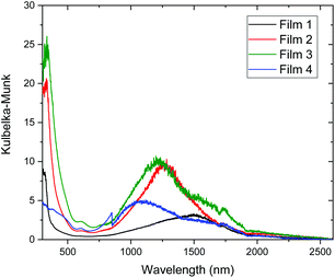 |
| | Fig. 10 Electronic absorption spectra of films 1–4. | |
Scanning electron microscopy
The morphology of the electrodeposited films was investigated using scanning electron microscopy (SEM) and representative images of the surface are shown in Fig. 11 and in the ESI (Fig. S9–S11†). The electrodeposition process results in the formation of non-crystalline films, consistent with the amorphous powder obtained via the chemical synthesis. At least two different morphologies are visible: firstly, interconnected and spherical aggregates are visible, with a size of approximately 5–10 μm. The size and density of these aggregates increases in accordance with increasing deposition time, consistent with the increase in molar surface coverage. Underneath these agglomerates a second morphology can be seen, that of flake-like plates which exist on portions of the films (ESI†). Upon increasing the magnification a third morphology becomes apparent, that of thin fibres (ESI†). Variation in the electrode surface (from films 1–3 to film 4) has a significant impact on the morphology of the resultant film; the surface of film 4 is mostly covered with the flake-like plates, with no sign of the spherical aggregates. On top of these plates a network of long thin fibres (20–100 nm) can be seen that are partially transparent to the electron beam. It is possible that the lower current observed for film 4 is due to the more complete coverage of the surface with these plates, which may be less conductive than the ITO or the fibrous morphology present in films 1–3.
 |
| | Fig. 11 SEM images of electrodeposited films (a) film 1, (b) film 2, (c) film 3 and (d) film 4. | |
Conclusions
To conclude, we report the synthesis of a new anionic gold dithiolene complex, NBu4·[1-i], and that of its corresponding neutral gold complex 2. The molecular optical and electrochemical properties of both complexes were investigated experimentally and agreed well with the theoretical calculations. In the solid state, complex 2 shows a strong absorption into the IR, corresponding to a small band gap of 0.5 eV determined by conductivity measurements on a compressed pellet, indicating strong intermolecular interactions in the solid state. These strong intermolecular interactions are also indicated by the weakly temperature dependent paramagnetic susceptibility of 2, and its insoluble nature. The conductivity of complex 2 also exhibited a pressure dependence, showing a 49 fold increase in conductivity on application of 2 GPa. Due to their highly insoluble nature, fabrication of thin films of neutral gold dithiolenes is not feasible by conventional methods. Here, we fabricated conductive thin films of 2via electrodeposition from the more soluble anion NBu4·[1-i], the first example of a neutral gold dithiolene complex processed into a thin film form. The films showed a variety of morphologies, from fibers to plaques to spherical aggregates, with strong absorptions out into the NIR, indicating that the strong intermolecular interactions were retained in the film.
Experimental
Materials, synthesis, and characterization
All commercially available chemicals were used without further purification. Ligand precursor 4-(4-phenylphenyl)-1,3-dithiol-2-one was prepared as described in the literature.54 Elemental analyses were carried out by Stephen Boyer of the Science Centre, London Metropolitan University using a Carlo Erba CE1108 Elemental Analyzer. NBu4·[1-i] NaOMe (1.00 g, 18.51 mmol) was added to a stirred solution of 4-(4-chlorophenyl)-1,3-dithiol-2-one (0.86 g, 3.70 mmol) in methanol/THF (15/5 ml) that had been degassed for 15 min with bubbling nitrogen. The mixture was stirred at RT for 1 h. The reaction mixture was heated to 50 °C and KAuCl4 (0.70 g, 1.85 mmol) was added. The mixture was stirred at 50 °C for 1 h before the solvent was removed in vacuo. The residue was redissolved in acetone (100 ml) and NBu4I (0.593 g, 1.84 mmol) was added. The mixture was stirred at RT overnight and the solvent was removed in vacuo. DCM (50 ml) and brine (50 ml) were added, and the layers separated. The aqueous layer was extracted with further DCM (3 × 20 ml), and the organic layers were combined, dried using magnesium sulfate, filtered and the solvent was removed in vacuo to give the anionic complex as a mixture of isomers, NBu4·[1]. The mixture was dissolved in acetone (100 ml) and isopropanol (75 ml) was then layered on top of the solution until precipitation was observed at the phase boundary. This was then left for 3 days. The crystalline precipitate was collected via filtration and washed with isopropanol to give the pure isomer NBu4·[1-i] (0.99 g, 40%); IR (ν/cm−1) 2960, 1562, 1537, 1478, 1456, 1409, 1394, 1378, 1077, 1066, 1057, 1010, 913, 898, 881, 841, 809, 777; δH (500 MHz; CD3CN; Me4Si) 7.56–7.54 (4H, dt, J 8.6, 2.0), 7.22–7.19 (4H, dt, J 8.6, 2.0), 6.71 (2H, s), 3.18–3.15 (8H, m), 1.58–1.53 (8H, m), 1.40–1.32 (8H, s, J 7.4), 0.95–0.92 (12H, t, J 7.3).
Complex
2 I2 (100 mg, 0.40 mmol) was added to a stirred solution of the NBu4·[1-i] (500 mg, 0.737 mmol) in acetone (50 ml) and the mixture was stirred at RT for 1 h. The precipitate formed was separated by centrifuge and washed with acetone until the supernatant liquid was colourless. The green-black powder was collected by filtration, 2 (0.15 g, 73.7%); IR (ν/cm−1) 1585, 1445, 1415, 1386, 1204, 1179, 1091, 1008, 930, 845, 818, 782, 768, 711, 650; anal. calcd for C18H16AuS4: C, 32.12; H, 1.68 found: C, 32.32; H, 1.71.
Optical characterisation
UV–vis-NIR solution absorption and diffuse reflectance measurements were recorded using a Jasco V-670 UV/vis/NIR spectrophotometer controlled with SpectraManager software. Solution state UV–visible absorption spectra were obtained using freshly prepared solutions of the complexes in acetonitrile (NBu4·[1-i]) and chloroform (2) at low concentrations (<10−5 M) in a 1 cm pathlength cell. Baseline correction was achieved by reference to pure solvent in the same cuvette. The Kubelka–Munk function was used to analyse the data collected from diffuse reflectance measurements and values of direct and indirect band gap of 2 were constructed using Tauc plots (ESI†).
Electrochemical characterization
Cyclic voltammetry experiments were recorded using an Autolab Type III potentiostat, and the results analysed using GPES electrochemical software. The instrument was fitted with a three-electrode system consisting of a Pt disk as the working electrode, and Pt wire as the auxiliary electrode and reference electrode, with ferrocene used as an internal reference. Experiments were conducted at room temperature in dry acetonitrile solution with n-Bu4NPF6 (0.1 M) as the supporting electrolyte. Cyclic voltammetry experiments were conducted at a scan rate of 100 mV s−1, unless otherwise specified. Each solution was purged with N2 prior to the experiment.
Magnetic characterization
Magnetic susceptibility measurements were performed on polycrystalline samples from 3 to 300 K using a Quantum Design Magnetic Property Measurement System (MPMS)-XL SQUID magnetometer with MPMS MultiVu Application software to process the data. The magnetic field used was 3 T. The paramagnetic susceptibility χp was calculated by correction with the diamagnetic contributions from the sample (Pascal's constants: −3.55 × 10⁻⁴ emu mol−1 (ref. 55)) and holder (a plastic straw).
Computational details
Neutral gold dithiolene complexes exist as mixed valence compounds, and their unpaired electron can either be localized over one dithiolene ligand (Robin-Day Classes I and II) or delocalized across the whole structure (Class III).50,56,57 This distinction between Class II and Class III structures can be difficult to reproduce with DFT methods, as due self-interaction errors many DFT functionals over-delocalise spin and electron density.58,59 With this in mind, DFT calculations for [trans-1]−, [cis-1]−, cis-2 and trans-2 carried out using the hybrid B3LYP functional,60,61 and the BHLYP35 functional, as described by Kaupp et al. for the treatment of mixed valence species.62,63 Both functionals resulted in a highly delocalised electron structure for both cis-2 and trans-2 (for BHLYP35 molecular orbitals, see ESI†), while TD-DFT calculations for BHLYP35 underestimated the SOMO-LUMO gap (exp. ∼1450 nm) even more severely than B3LYP (∼2100 nm for BHLYP35 vs. ∼1620 nm for B3LYP). As a result, the B3LYP results are reported here, while the BHLYP35 results are placed in the ESI.† DFT calculations were performed using the Gaussian09 package,64 with analysis of the molecular orbitals and the TD-DFT conducted with GaussSum.65 In all cases, the 6-31+G** basis sets were used for H, C, S and Cl,66,67 and the LanL2DZ basis set and Los Alamos effective core potentials for Au.68–71 Electronic structure and calculations were conducted from the optimised geometries.
Conductivity measurements: ambient pressure
The conductivity of 2 was investigated using the 4-probe method on a compressed pellet of the powder. Four copper wires were attached to the compressed pellet (∅ = 3 mm, thickness = 0.43 mm) using silver paint. To investigate the effect of temperature, the pellet was glued to a puck and placed into a physical property measurement system (PPMS) to allow for controlled cooling. The PPMS was subsequently cooled to 190 K at 5 K min−1, with the temperature allowed to equilibrate for 10 s at each 5 K interval to allow for resistivity readings.
Conductivity measurements: elevated pressures
Ambient temperature, varying pressure measurements were conducted on a compressed pellet of 2 (∅ = 3 mm, thickness = 0.43 mm) in a piston-cylinder cell apparatus using Daphne Oil as the (hydrostatic) pressure transmitting medium. The pressure inside the cell was measured using the resistance of manganin wire, which was read using the 4-probe method using a Keithley multimeter (KEITHLEY® 2002 digital multimeter). As sample geometry and contact separation were not affected by pressure application resistance was converted to resistivity via the Montgomery method.72 Further experimental details are available in the ESI.†
Electrodeposition of thin films
A 3 electrode cell was set up with two platinum wires as the reference and counter electrode and a piece of FTO glass (films 1–3) or FTO glass coated with Pt (film 4) as the working electrode. This was attached to the cell by placing a thin layer of aluminium foil around one of its edges and attaching a crocodile clip to the slide. The glass was then partially submerged in a solution of 1 mM NBu4·[1-i] in acetonitrile, using 0.1 M [TBA][PF6] as the background electrolyte. The potential applied was held at 0.29 V (vs. Fc+/Fc), which was sufficient to oxidise NBu4·[1-i]. The potential was held for 10, 20 and 40 min for films 1–3 respectively, and 30 min for film 4. Following the deposition, the films were immersed into a fresh acetonitrile solution for 3 minutes to remove residual electrolyte species from the film. Afterwards, the films were dried in vacuo overnight.
For film 4 the surface of the FTO glass was platinized using Platisol T/SP (Solaronix, Swiss) by doctor-blading and heated to 400 °C for 15 min.
Scanning electron microscopy
SEM images were collected using a Carl Zeiss SIGMA HD VP Field Emission SEM, operated in InLens mode with a 10 kV accelerating voltage.
Conflicts of interest
There are no conflicts to declare.
Acknowledgements
The authors thank the Leverhulme Trust (RPG–2016–152) for funding. This work has made use of the resources provided by the Edinburgh Compute and Data Facility (ECDF) (http://www.ecdf.ed.ac.uk/).
Notes and references
- R. Kato, Chem. Rev., 2004, 104, 5319–5346 CrossRef CAS.
- N. Robertson and L. Cronin, Coord. Chem. Rev., 2002, 227, 93–127 CrossRef CAS.
- S. Dalgleish, M. M. Matsushita, L. Hu, B. Li, H. Yoshikawa and K. Awaga, J. Am. Chem. Soc., 2012, 134, 12742–12750 CrossRef CAS.
- P. Deplano, L. Pilia, D. Espa, M. L. Mercuri and A. Serpe, Coord. Chem. Rev., 2010, 254, 1434–1447 CrossRef CAS.
- S. Dalgleish, J. G. Labram, Z. Li, J. Wang, C. R. McNeill, T. D. Anthopoulos, N. C. Greenham and N. Robertson, J. Mater. Chem., 2011, 21, 15422 RSC.
- L. Qu, Y. Guo, H. Luo, C. Zhong, G. Yu, Y. Liu and J. Qin, Chem. Commun., 2012, 48, 9965 RSC.
- G. C. Papavassiliou, G. C. Anyfantis and G. A. Mousdis, Crystals, 2012, 2, 762–811 CrossRef CAS.
- Y. Le Gal, T. Roisnel, P. Auban-Senzier, N. Bellec, J. Íñiguez, E. Canadell and D. Lorcy, J. Am. Chem. Soc., 2018, 140, 6998–7004 CrossRef CAS.
- W. Suzuki, E. Fujiwara, A. Kobayashi, Y. Fujishiro, E. Nishibori, M. Takata, M. Sakata, H. Fujiwara and H. Kobayashi, J. Am. Chem. Soc., 2003, 125, 1486–1487 CrossRef CAS.
- B. Zhou, M. Shimamura, E. Fujiwara, A. Kobayashi, T. Higashi, E. Nishibori, M. Sakata, H. Cui, K. Takahashi and H. Kobayashi, J. Am. Chem. Soc., 2006, 128, 3872–3873 CrossRef CAS.
- H. Tanaka, S. Hara, M. Tokumoto, A. Kobayashi and H. Kobayashi, Chem. Lett., 2007, 36, 1006–1007 CrossRef CAS.
- S. Ishibashi, H. Tanaka, M. Kohyama, M. Tokumoto, A. Kobayashi, H. Kobayashi and K. Terakura, J. Phys. Soc. Jpn., 2005, 74, 843–846 CrossRef CAS.
- Y. Hara, K. Miyagawa, K. Kanoda, M. Shimamura, B. Zhou, A. Kobayashi and H. Kobayashi, J. Phys. Soc. Jpn., 2008, 77, 53706 CrossRef.
- S. Ishibashi, K. Terakura and A. Kobayashi, J. Phys. Soc. Jpn., 2008, 77, 024702 CrossRef.
- M. Tsuchiizu, Y. Omori, Y. Suzumura, M.-L. Bonnet and V. Robert, J. Chem. Phys., 2012, 136, 044519 CrossRef.
- M. Bousseau, L. Valade, J. P. Legros, P. Cassoux, M. Garbauskas and L. V. Interrante, J. Am. Chem. Soc., 1986, 108, 1908–1916 CrossRef CAS.
- L. Brossard, M. Ribault, L. Valade, P. Cassoux, M. Staff, H. Commiti, E. E. On, T. H. E. Judiciary and I. Memorandum, Phys. B+C, 1986, 143, 378–380 CrossRef CAS.
- D. de Caro, I. Malfant, J.-P. Savy and L. Valade, J. Phys.: Condens. Matter, 2008, 20, 184012 CrossRef.
- S. G. Liu, Y. Q. Liu and D. Ben Zhu, Synth. Met., 1997, 86, 2265–2266 CrossRef CAS.
- S. Dalgleish, H. Yoshikawa, M. M. Matsushita, K. Awaga and N. Robertson, Chem. Sci., 2011, 2, 316–320 RSC.
- S. Dalgleish, K. Awaga and N. Robertson, Chem. Commun., 2011, 47, 7089 RSC.
- E. Allwright, G. Silber, J. Crain, M. M. Matsushita, K. Awaga and N. Robertson, Dalton Trans., 2016, 45, 9363–9368 RSC.
- E. Allwright, D. M. Berg, R. Djemour, M. Steichen, P. J. Dale and N. Robertson, J. Mater. Chem. C, 2014, 2, 7232–7238 RSC.
- N. Tenn, N. Bellec, O. Jeannin, L. Piekara-Sady, P. Auban-Senzier, J. Íñiguez, E. Canadell and D. Lorcy, J. Am. Chem. Soc., 2009, 131, 16961–16967 CrossRef CAS.
- P. Stoliar, P. Diener, J. Tranchant, B. Corraze, B. Brière, V. Ta-Phuoc, N. Bellec, M. Fourmigué, D. Lorcy, E. Janod and L. Cario, J. Phys. Chem. C, 2015, 119, 2983–2988 CrossRef CAS.
- Y. Le Gal, T. Roisnel, P. Auban-Senzier, T. Guizouarn and D. Lorcy, Inorg. Chem., 2014, 53, 8755–8761 CrossRef CAS.
- G. Yzambart, N. Bellec, G. Nasser, O. Jeannin, T. Roisnel, M. Fourmigué, P. Auban-Senzier, J. Íñiguez, E. Canadell and D. Lorcy, J. Am. Chem. Soc., 2012, 134, 17138–17148 CrossRef CAS.
- A. Mizuno, H. Benjamin, Y. Shimizu, Y. Shuku, M. M. Matsushita, N. Robertson and K. Awaga, Adv. Funct. Mater., 2019, 29, 1904181 CrossRef CAS.
- A. Filatre-Furcate, N. Bellec, O. Jeannin, P. Auban-Senzier, M. Fourmigué, J. Íñiguez, E. Canadell, B. Brière, V. Ta Phuoc and D. Lorcy, Inorg. Chem., 2016, 55, 6036–6046 CrossRef CAS.
- M. A. Mazid, M. T. Razi and P. J. Sadler, Inorg. Chem., 1981, 20, 2872–2877 CrossRef CAS.
- J. M. Tunney, A. J. Blake, E. S. Davies, J. McMaster, C. Wilson and C. D. Garner, Polyhedron, 2006, 25, 591–598 CrossRef CAS.
- S. Rabaça, A. C. Cerdeira, S. Oliveira, I. C. Santos, R. T. Henriques, L. C. J. Pereira, J. T. Coutinho and M. Almeida, Polyhedron, 2012, 39, 91–98 CrossRef.
- A. Filatre-Furcate, P. Auban-Senzier, M. Fourmigué, T. Roisnel, V. Dorcet and D. Lorcy, Dalton Trans., 2015, 44, 15683–15689 RSC.
- T. Higashino, O. Jeannin, T. Kawamoto, D. Lorcy, T. Mori and M. Fourmigué, Inorg. Chem., 2015, 54, 9908–9913 CrossRef CAS.
- K. Ray, T. Weyhermüller, A. Goossens, M. W. J. Crajé and K. Wieghardt, Inorg. Chem., 2003, 42, 4082–4087 CrossRef CAS.
- L. Ambrosio, M. C. Aragoni, M. Arca, F. A. Devillanova, M. B. Hursthouse, S. L. Huth, F. Isaia, V. Lippolis, A. Mancini and A. Pintus, Chem. – Asian J., 2010, 5, 1395–1406 CAS.
- M. C. Aragoni, M. Arca, F. A. Devillanova, F. Isaia, V. Lippolis and A. Pintus, Chem. – Asian J., 2011, 6, 198–208 CrossRef CAS.
- S. Kokatam, K. Ray, J. Pap, E. Bill, W. E. Geiger, R. J. LeSuer, P. H. Rieger, T. Weyhermüller, F. Neese and K. Wieghardt, Inorg. Chem., 2007, 46, 1100–1111 CrossRef CAS.
- G. C. Papavassiliou, G. C. Anyfantis, N. Ioannidis, V. Petrouleas, P. Paraskevopoulou, C. P. Raptopoulou, V. Psycharis, N. Ioannidis, V. Petrouleas and P. Paraskevopoulou, Polyhedron, 2009, 28, 3368–3372 CrossRef CAS.
- R. Perochon, P. Davidson, S. Rouzière, F. Camerel, L. Piekara-Sady, T. Guizouarn and M. Fourmigué, J. Mater. Chem., 2011, 21, 1416–1422 RSC.
- D. Grujicic and B. Pesic, Electrochim. Acta, 2002, 47, 2901–2912 CrossRef CAS.
- S. Rodrigues, A. K. Shukla and N. Munichandraiah, J. Appl. Electrochem., 1998, 28, 1235–1241 CrossRef CAS.
- A. Filatre-Furcate, T. Roisnel, M. Fourmigué, O. Jeannin, N. Bellec, P. Auban-Senzier and D. Lorcy, Chem. – Eur. J., 2017, 23, 16004–16013 CrossRef CAS.
- N. C. Schiodt, P. Sommer-Larsen, T. Bjornholm, M. F. Nielsen, J. Larsen and K. Bechgaard, Inorg. Chem., 1995, 34, 3688–3694 CrossRef CAS.
- G.-E. Matsubayashi and A. Yokozawa, J. Chem. Soc., Dalton Trans., 1990, 3535–3539 RSC.
- D. Belo, H. Alves, E. Branco Lopes, M. T. Duarte, V. Gama, R. Teives Henriques, M. Almeida, A. Pérez-Benítez, C. Rovira and J. Veciana, Chem. – Eur. J., 2001, 7, 511–519 CrossRef CAS.
- A. Filatre-Furcate, N. Bellec, O. Jeannin, P. Auban-Senzier, M. Fourmigué, A. Vacher and D. Lorcy, Inorg. Chem., 2014, 53, 8681–8690 CrossRef CAS.
- B. Brière, J. Caillaux, Y. Le Gal, D. Lorcy, S. Lupi, A. Perucchi, M. Zaghrioui, J. C. Soret, R. Sopracase and V. Ta Phuoc, Phys. Rev. B, 2018, 97, 035101 CrossRef.
- H. Cui, H. Kobayashi, S. Ishibashi, M. Sasa, F. Iwase, R. Kato and A. Kobayashi, J. Am. Chem. Soc., 2014, 136, 7619–7622 CrossRef CAS.
- D. G. Branzea, F. Pop, P. Auban-Senzier, R. Clérac, P. Alemany, E. Canadell and N. Avarvari, J. Am. Chem. Soc., 2016, 138, 6838–6851 CrossRef CAS.
- R. Perochon, L. Piekara-Sady, W. Jurga, R. Clérac and M. Fourmigué, Dalton Trans., 2009, 3052–3061 RSC.
- I. A. Wright, C. Wilson, S. J. Coles and P. J. Skabara, Dalton Trans., 2019, 48, 107–116 RSC.
- K. Ray, T. Weyhermüller, F. Neese and K. Wieghardt, Inorg. Chem., 2005, 44, 5345–5360 CrossRef CAS.
- V. Madhu and S. K. Das, Inorg. Chem., 2008, 47, 5055–5070 CrossRef CAS.
- G. A. Bain and J. F. Berry, J. Chem. Educ., 2008, 85, 532 CrossRef CAS.
-
M. B. Robin and P. Day, in Advances in Inorganic Chemistry and Radiochemistry, 1968, vol. 10, pp. 247–422 Search PubMed.
- M. M. Andrade, R. A. L. Silva, I. C. Santos, E. B. Lopes, S. Rabaça, L. C. J. Pereira, J. T. Coutinho, J. P. Telo, C. Rovira, M. Almeida and D. Belo, Inorg. Chem. Front., 2017, 4, 270–280 RSC.
- E. R. Johnson, P. Mori-Sánchez, A. J. Cohen and W. Yang, J. Chem. Phys., 2008, 129, 204112 CrossRef.
- T. Heaton-Burgess and W. Yang, J. Chem. Phys., 2010, 132, 234113 CrossRef.
- A. D. Becke, J. Chem. Phys., 1993, 98, 5648–5652 CrossRef CAS.
- C. Lee, W. Yang and R. G. Parr, Phys. Rev. B: Condens. Matter Mater. Phys., 1988, 37, 785–789 CrossRef CAS.
- M. Kaupp, M. Renz, M. Parthey, M. Stolte, F. Würthner and C. Lambert, Phys. Chem. Chem. Phys., 2011, 13, 16973–16986 RSC.
- M. Parthey and M. Kaupp, Chem. Soc. Rev., 2014, 43, 5067–5088 RSC.
-
M. J. Frisch, G. W. Trucks, H. B. Schlegel, G. E. Scuseria, M. A. Robb, J. R. Cheeseman, G. Scalmani, V. Barone, G. A. Petersson, H. Nakatsuji, X. Li, M. Caricato, A. Marenich, J. Bloino, B. G. Janesko, R. Gomperts, B. Mennucci, H. P. Hratchian, J. V. Ortiz, A. F. Izmaylov, J. L. Sonnenberg, D. Williams-Young, F. Ding, F. Lipparini, F. Egidi, J. Goings, B. Peng, A. Petrone, T. Henderson, D. Ranasinghe, V. G. Zakrzewski, J. Gao, N. Rega, G. Zheng, W. Liang, M. Hada, M. Ehara, K. Toyota, R. Fukuda, J. Hasegawa, M. Ishida, T. Nakajima, Y. Honda, O. Kitao, H. Nakai, T. Vreven, K. Throssell, J. A. J. Montgomery, J. E. Peralta, F. Ogliaro, M. Bearpark, J. J. Heyd, E. Brothers, K. N. Kudin, V. N. Staroverov, T. Keith, R. Kobayashi, J. Normand, K. Raghavachari, A. Rendell, J. C. Burant, S. S. Iyengar, J. Tomasi, M. Cossi, J. M. Millam, M. Klene, C. Adamo, R. Cammi, J. W. Ochterski, R. L. Martin, K. Morokuma, O. Farkas, J. B. Foresman and D. J. Fox, Gaussian 09, Revision A.02 Search PubMed.
- N. M. O'Boyle, A. L. Tenderholt and K. M. Langner, J. Comput. Chem., 2008, 29, 839–845 CrossRef.
- G. A. Petersson, A. Bennett, T. G. Tensfeldt, M. A. Al-Laham, W. A. Shirley and J. Mantzaris, J. Chem. Phys., 1988, 89, 2193–2218 CrossRef CAS.
- G. A. Petersson and M. A. Al-Laham, J. Chem. Phys., 1991, 94, 6081–6090 CrossRef CAS.
-
T. H. Dunning and P. J. Hay, in Methods of Electronic Structure Theory, ed. H. F. Schaefer, Springer US, Boston, MA, 1977, pp. 1–27 Search PubMed.
- P. J. Hay and W. R. Wadt, J. Chem. Phys., 1985, 82, 299–310 CrossRef CAS.
- P. J. Hay and W. R. Wadt, J. Chem. Phys., 1985, 82, 270–283 CrossRef CAS.
- W. R. Wadt and P. J. Hay, J. Chem. Phys., 1985, 82, 284–298 CrossRef CAS.
- H. C. Montgomery, J. Appl. Phys., 1971, 42, 2971–2975 CrossRef CAS.
Footnote |
| † Electronic supplementary information (ESI) available: NMR; PXRD; CV; high-P conductivity; (TD)DFT; electronic absorption; SEM. See DOI: 10.1039/d0dt02174a |
|
| This journal is © The Royal Society of Chemistry 2020 |
Click here to see how this site uses Cookies. View our privacy policy here. 
 Open Access Article
 This Open Access Article is licensed under a Creative Commons Attribution-Non Commercial 3.0 Unported Licence
 *a
*a


