
 Open Access Article
 This Open Access Article is licensed under a
 Creative Commons Attribution 3.0 Unported Licence
Photoelectrochemical water-splitting over a surface modified p-type Cr2O3 photocathode†
Keita
Sekizawa
 *,
Keiichiro
Oh-ishi
and
Takeshi
Morikawa
*,
Keiichiro
Oh-ishi
and
Takeshi
Morikawa
Toyota Central R&D Laboratories, Inc., 41-1, Yokomichi, Nagakute, Aichi 480-1192, Japan. E-mail: sekizawa@mosk.tytlabs.co.jp
First published on 28th November 2019
Abstract
Cr2O3 is a p-type semiconductor with a negative conduction band minimum position suitable for photocathodic H2 generation. Therefore, Cr2O3 is a candidate photocathode material for photoelectrochemical (PEC) water-splitting. However, Cr2O3 has not yet been applied for the purpose of H2 generation because the efficiency and stability of the photocurrent generated by a Cr2O3 electrode are poor, due to high defect and vacancy concentrations. In the present work, the Cr2O3 surface was modified with n-type TiO2 after which Pt particles were deposited to catalyse H2 production. The TiO2 overlayer passivated the Cr2O3 surface states that otherwise cause deleterious interactions with the Pt particles. This layer also improved charge separation from the conduction band of Cr2O3 to the Pt co-catalyst, by forming a p–n junction. As a result of the TiO2 insertion, the cathodic photocurrent resulting from light absorption by Cr2O3 was enhanced and stabilized. This represents the first-ever use of Cr2O3 as a light-absorbing material in a multi-layered electrode to accomplish PEC water-splitting for H2 generation.
Introduction
H2 has attracted considerable interest as a clean energy carrier that does not produce CO2, and is expected to play an important role in meeting growing worldwide energy requirements.1–3 Photoelectrochemical (PEC) water-splitting into H2 and O2 using semiconductor electrodes is a promising approach to the direct conversion of solar energy into H2.4–6 In 1972, Honda and Fujishima first reported the PEC decomposition of water to H2, utilizing an n-type TiO2 electrode in conjunction with UV illumination and the application of an external electrical bias.7 After this pioneering work, numerous semiconductor photocatalysts and photoelectrodes were developed.8–17 It is widely recognized that most semiconductors require the addition of a sacrificial electron donor or the application of an external voltage, as the edges of the conduction band and valence band typically do not straddle the water reduction and oxidation potentials. As a means of promoting water splitting without an external electrical bias while separately generating H2 and O2 at different electrodes, PEC devices containing electrically connected p-type and n-type semiconductor photoelectrodes have been designed.18–22 Metal oxides are suitable semiconductor materials because they are abundant and relatively inexpensive. Since metal oxide semiconductors predominantly exhibit n-type characteristics, because they readily form oxygen vacancies, there have been many reports regarding the use of n-type semiconductor photoanodes to generate oxygen. In contrast, there are only a few native p-type semiconductor oxides, because the cation vacancies or oxygen interstitials that produce p-type conductivity are not easily generated.23,24 Moreover, utilizing photocathodes for H2 evolution requires that the conduction band minimum of the cathode material be more negative than the H+/H2 reduction potential (0 V vs. reversible hydrogen electrode; RHE). The oxide p-type semiconductors meeting this requirement are limited, with examples being copper oxides25,26 and iron oxides.27–29Cr2O3 is one of the few oxides exhibiting p-type conductivity.30,31 Standard Cr2O3 has a hexagonal corundum structure.32,33 In the unit cell of non-defective Cr2O3, two-thirds of the octahedral oxygen sites are occupied by Cr while the remaining one-third are unoccupied (Fig. S1†). Consequently, removing Cr atoms from the cell generates vacancies. Moreover, the migration of Cr to the pre-existing empty sites (typically interstitial sites in nearby locations) results in Cr Frenkel defects, while the diffusion of O atoms generates O vacancies. These defects and vacancies are known to determine the appearance of p-type and n-type characteristics.34–38 The defect formation energy values calculated using first-principles DFT+U by Diawara et al.38 suggest that the stability of defects follows the order: Cr Frenkel defect > Cr vacancy > O vacancy. Therefore, native Cr2O3 tends to form metal-deficient sites that result in p-type conductivity. The p-type conductivity of Cr2O3 has been applied to produce hole transfer layers inserted between a back contact and a semiconductor photoabsorber, such as CuO26 or Fe2O3.39 Moreover, the conduction band minimum of Cr2O3 is located at a much more negative level than the redox potential for water reduction.40,41 Even so, to the best of our knowledge, there have been no reports of the application of Cr2O3 as a photoabsorber in photocathodes for H2 generation. This may be due to the ready formation of various defects and vacancies in Cr2O3. Defects, vacancies and surface dangling bonds form states within the bandgap that can serve as recombination centres for photogenerated charges (Scheme 1a). In addition, a high density of bandgap states will transition Cr2O3 into a conductor.42,43 However, if photogenerated charges can be prevented from transferring to such bandgap states, it may be possible to apply Cr2O3 as a photocathode for H2 evolution. Furthermore, since band gap narrowing via doping with specific ions has already been realized,44–47 Cr2O3 also has the potential to become a visible-light responsive photocathode.
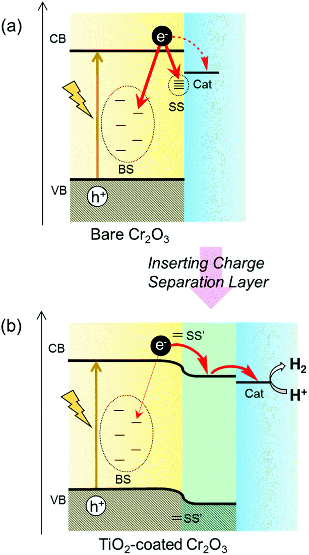 | ||
| Scheme 1 Schematic diagram of the expected electron transfer process in (a) bare Cr2O3 and (b) TiO2-coated Cr2O3 photocathodes. BS and SS indicate bulk states and surface states, respectively. The former are generated by defects and vacancies, while the latter result from surface dangling bonds. | ||
Recently, it has been reported that various benefits can be obtained by the surface treatment of photoelectrodes.48,49 Specifically, such processing can protect the unstable surface of the photoabsorber from photocorrosion by preventing contact with the electrolyte. Furthermore, this treatment can passivate surface states. When the atomic orbitals of surface states couple with those of deposits, the coupled surface states can be moved away from the band gap because of the formation of bonding and antibonding states49 (shown as SS′ in Scheme 1b). Moreover, the formation of a heterojunction by surface treatment is expected to modify band bending due to the diffusion of charge carriers between two semiconductors having different Fermi levels. This modification should enhance both photogenerated electron–hole separation and carrier transfer. Therefore, in the present work, the Cr2O3 surface was modified with n-type TiO2 to ensure both charge separation and passivation. Subsequently, Pt particles were deposited on the TiO2 layer to catalyse H2 production50 (Scheme 1b).
Results and discussion
Structural and optical properties of Cr2O3
Cr2O3 electrodes were prepared by the radio frequency (RF) reactive magnetron sputtering of Cr targets in an Ar/O2 (9![[thin space (1/6-em)]](https://www.rsc.org/images/entities/char_2009.gif) :1) plasma to give a thickness of 60 nm on a transparent conductive oxide (TCO; SnO2-coated indium tin oxide (ITO)), followed by annealing at 823 K. As shown in Fig. 1 (blue line), the X-ray diffraction (XRD) patterns of the resulting Cr2O3 on TCO exhibit peaks at 33.8°, 36.4° and 55.3°, which are assignable to the (104), (110) and (116) diffractions of Cr2O3 (eskolaite), respectively. All other peaks are attributed to SnO2 or ITO, while there are no peaks due to impurities. The X-ray photoelectron spectroscopy (XPS) data obtained from the resulting Cr2O3 layer are presented in Fig. 2a, and are similar to those produced by the reference Cr2O3 (Fig. 2c). The peaks at binding energies of 576.5 and 586.1 eV are ascribed to the Cr 2p3/2 and 2p1/2 signals of Cr(III) oxide, respectively. Although the Cr 2p3/2 peak includes a shoulder, this peak shape is typical of Cr2O3 and is attributed to the multiplet structure of Cr(III) oxide.51 Pt was subsequently deposited on the electrodes as a co-catalyst for H2 evolution from water by sputtering, to a nominal thickness of 1 nm. Scanning transmission electron microscopy (STEM) combined with energy-dispersive X-ray spectroscopy (EDX) for elemental mapping was used to assess cross-sections of the Pt/Cr2O3 sample, as shown in Fig. 3a. In both electrodes, a flat Cr2O3 layer was observed on the TCO film.
:1) plasma to give a thickness of 60 nm on a transparent conductive oxide (TCO; SnO2-coated indium tin oxide (ITO)), followed by annealing at 823 K. As shown in Fig. 1 (blue line), the X-ray diffraction (XRD) patterns of the resulting Cr2O3 on TCO exhibit peaks at 33.8°, 36.4° and 55.3°, which are assignable to the (104), (110) and (116) diffractions of Cr2O3 (eskolaite), respectively. All other peaks are attributed to SnO2 or ITO, while there are no peaks due to impurities. The X-ray photoelectron spectroscopy (XPS) data obtained from the resulting Cr2O3 layer are presented in Fig. 2a, and are similar to those produced by the reference Cr2O3 (Fig. 2c). The peaks at binding energies of 576.5 and 586.1 eV are ascribed to the Cr 2p3/2 and 2p1/2 signals of Cr(III) oxide, respectively. Although the Cr 2p3/2 peak includes a shoulder, this peak shape is typical of Cr2O3 and is attributed to the multiplet structure of Cr(III) oxide.51 Pt was subsequently deposited on the electrodes as a co-catalyst for H2 evolution from water by sputtering, to a nominal thickness of 1 nm. Scanning transmission electron microscopy (STEM) combined with energy-dispersive X-ray spectroscopy (EDX) for elemental mapping was used to assess cross-sections of the Pt/Cr2O3 sample, as shown in Fig. 3a. In both electrodes, a flat Cr2O3 layer was observed on the TCO film.
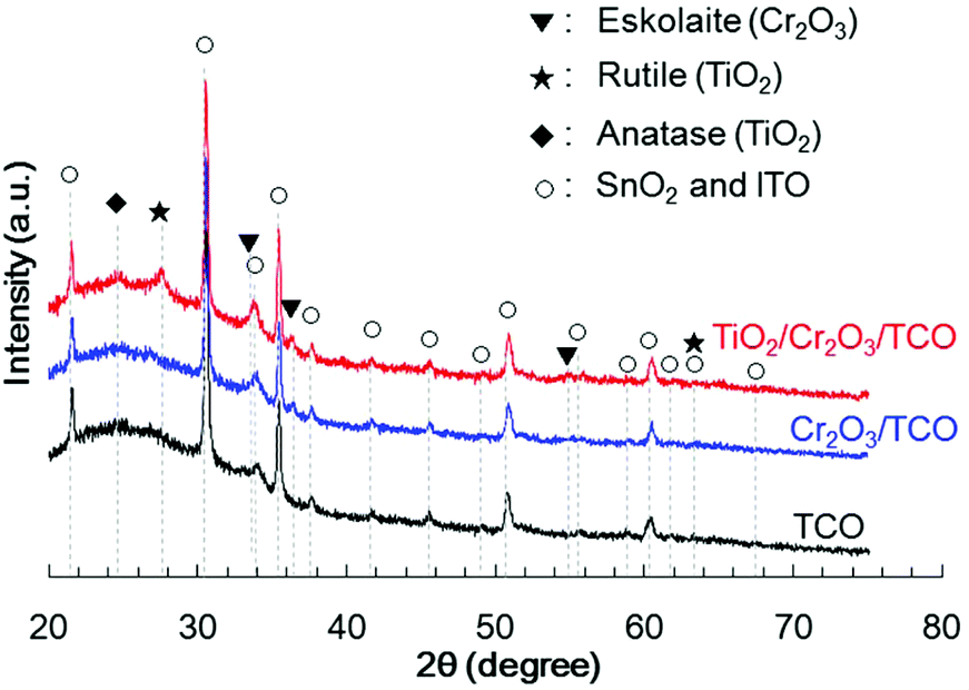 | ||
| Fig. 1 XRD patterns obtained from TCO (black line), Cr2O3/TCO (blue line) and TiO2/Cr2O3/TCO (red line). | ||
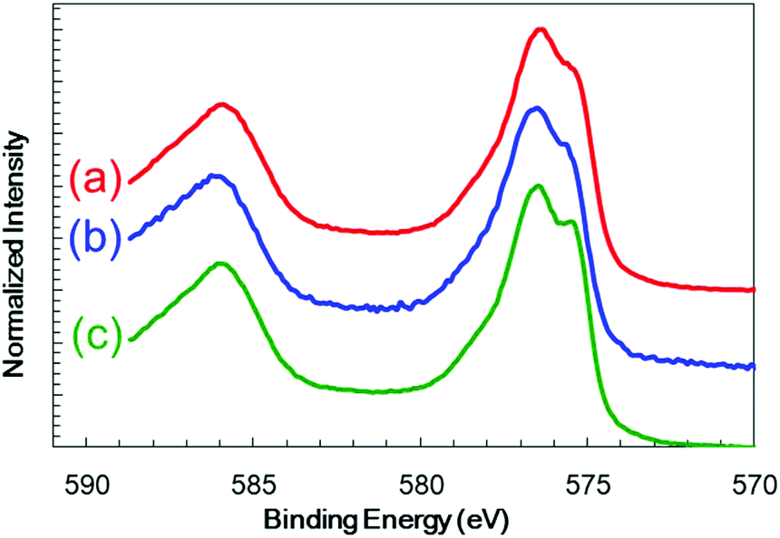 | ||
| Fig. 2 XPS spectra obtained from a Cr2O3 electrode (a) before and (b) after photoelectrolysis for 1 h and from (c) the reference Cr2O3. | ||
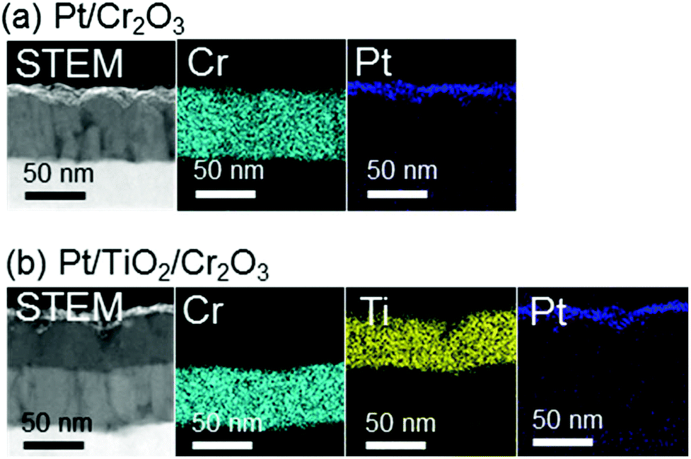 | ||
| Fig. 3 Cross-sectional STEM images and STEM-EDX elemental maps for (a) Pt/Cr2O3 and (b) Pt/TiO2/Cr2O3. | ||
UV/visible absorption spectra were acquired by a transmission method for this electrode and are shown in Fig. 4 as a blue line. Although an interference spectrum was included in the original spectrum, the absorption edge is evident at 410 nm, in agreement with a Cr2O3 reference bulk powder (Fig. S2†) and previous reports52–54
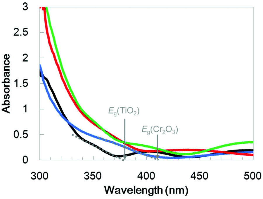 | ||
| Fig. 4 UV/visible absorption spectra for TiO2/Cr2O3 (red line), Cr2O3 (blue line) and TiO2 (black line) on TCO and the sum of the Cr2O3 and TiO2 spectra (green line). Eg indicates the absorption edges for the band-gap excitation. | ||
PEC properties of the Cr2O3 electrodes
Fig. 5a and b present the current–potential curves obtained from the Cr2O3-based electrodes and from a TiO2 electrode in a 0.5 M Na2CO3:NaHCO3 (1:1) buffer electrolyte (pH 9.7) under chopped AM 1.5 irradiation (1 Sun; 100 mW cm−2), with irradiation of the deposited semiconductor side. The bare Cr2O3 electrode (Fig. 5a, black line) generated a cathodic photocurrent in the negative voltage range below +1.1 V vs. RHE, although it also produced a dark current. The photocurrent density of this sample at +0.1 V, after removing the dark current density from the current density produced during light irradiation, was −15 μA cm−2. This cathodic photocurrent indicates that the Cr2O3 electrode exhibited p-type conductivity and could possibly be utilized as a photocathode for water splitting. However, a large cathodic dark current was apparent between +1.1 and +1.5 V, including a peak of −240 μA cm−2 at +1.08 V. This significant dark current indicates that electrons leaked to defect states and surface states in the band gap. Upon applying a constant potential of +0.11 V vs. RHE, the dark current was decreased due to electron charging, while the cathodic photocurrent was observed to decay from 8.1 to 0.9 μA cm−2 during 1 sun irradiation for 3 min (Fig. 5c, black line). After 1 h of photoelectrolysis, the dark current was slightly increased but the difference in the photocurrent in the current–potential curve was negligible (Fig. S3†). In addition, when the chemical state of the Cr2O3 surface was examined by XPS, there were almost no differences before and after the photoelectrolysis (Fig. 2a and b, respectively), suggesting no self-reduction of Cr2O3 by the photogenerated electrons. Therefore, Cr2O3 itself was stable during photoelectrolysis but photoelectrons could be trapped in defects and surface states, resulting in photocurrent decay.
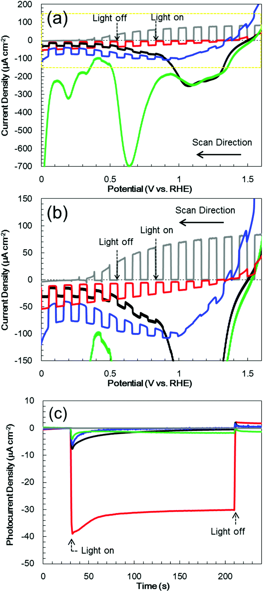 | ||
| Fig. 5 (a) Photocurrent–potential characteristics under chopped light irradiation, (b) enlargement of the area in the yellow dotted line in (a), and (c) photocurrent transients at +0.11 V vs. RHE in a 0.5 M Na2CO3:NaHCO3 (1:1) buffer electrolyte (pH 9.7) under one sun (100 mW cm−2, AM 1.5) illumination for the bare Cr2O3 (black line), Pt/Cr2O3 (green line), TiO2 (grey line), TiO2/Cr2O3 (blue line) and Pt/TiO2/Cr2O3 (red line). | ||
Pt was deposited on Cr2O3 as a co-catalyst for H2 evolution, by sputtering. The current–potential curve produced by the resulting Pt/Cr2O3 exhibited a new and significant dark current between 0.5 and 0.9 V, including a peak of −700 μA cm−2 at +0.63 V. Moreover, the photocurrent was negligible after Pt loading (Fig. 5a, green line). Although the dark current was reduced by applying a constant potential of +0.11 V vs. RHE under dark conditions, the photocurrent was smaller than that obtained from pure Cr2O3 (Fig. 5c, green line). The large dark current in the current–potential curve suggests that new band-gap states were generated within the bandgap of Cr2O3 following Pt deposition. The appearance of these deleterious band gap states can possibly be ascribed to the coupling of the atomic orbitals of dangling atoms at the Cr2O3 surface with those of deposited Pt atoms. The resulting bonding and antibonding orbitals would generate deleterious band-gap states,55 leading to electron leakage and recombination of photo-generated electrons and holes. As a result, the addition of Pt nanoparticles to the Cr2O3 surface diminished the photocurrent without acting as a co-catalyst for H2 evolution.
Coating with TiO2 as passivation and charge-separation layer
TiO2 overlayers with thicknesses ranging from 10 to 120 nm were subsequently deposited by sputtering a TiO2 target in an Ar/O2 (4:1) plasma onto Cr2O3. This was followed by post-annealing at 748 K. The XRD patterns generated by TiO2/Cr2O3/TCO (Fig. 1, red line) exhibit peaks attributable to anatase (101), and rutile (110) and (310) diffractions at 24.8°, 27.8° and 63.4°, respectively. In the STEM-EDX images for the Pt/TiO2/Cr2O3 electrode (Fig. 3b), the TiO2 layer completely covered the Cr2O3 surface, preventing contact with both the Pt and the electrolyte. The UV/visible absorption spectrum of the TiO2/Cr2O3 electrode was essentially consistent with the sum of the spectra of the TiO2 and Cr2O3 electrodes (Fig. 4, grey dotted line). The absorption edge of the TiO2 electrode (Fig. 4, black line) was observed at 380 nm, consistent with a TiO2 reference bulk powder (Fig. S2†) and the previous report.56 These data indicate that simulated solar radiation imparted to the TiO2 side should be absorbed by both TiO2 and Cr2O3.
In photocurrent-potential curves, the surface of Cr2O3 was subsequently coated with a 60 nm thick TiO2 layer. The resulting TiO2/Cr2O3 photocathode generated a cathodic photocurrent below +1.1 V (Fig. 5b, blue line). The photocurrent at +0.1 V was −35 μA cm−2, and so exceeded that obtained from the bare Cr2O3 (−15 μA cm−2). Although the TiO2 electrode (without Cr2O3) exhibited an anodic photocurrent at values more positive than +0.3 V (Fig. 5b, grey line), the photocurrent of TiO2/Cr2O3 cannot be explained as a combination of those for TiO2 and Cr2O3. The cathodic photocurrent produced by TiO2/Cr2O3 was also larger than that for Cr2O3. The anodic photocurrent produced by TiO2/Cr2O3 was smaller and appeared at a more positive potential than that for TiO2. This positive shift of the onset potential for the anodic photocurrent can be explained by the formation of a p–n junction. The Fermi level of the n-type TiO2 would be expected to be shifted positively following the formation of a junction with the p-type Cr2O3 because the Fermi levels of TiO2 and Cr2O3 would be equalized by carrier diffusion. Moreover, the Cr2O3 layer would be expected to inhibit photogenerated electron transfer from TiO2 to TCO, because the conduction band minimum of Cr2O3 is higher than that of TiO2. Hence, TiO2/Cr2O3 generated a cathodic photocurrent. Moreover, the dark current produced by TiO2/Cr2O3 decreased, from −240 to −100 μA cm−2, by the TiO2 coating, indicating a decrease in the electron transfer to the band-gap states. Since the recombination of photo-generated electrons and holes at the band-gap states was suppressed, the photocurrent was enhanced by the TiO2 coating. However, at a constant potential of +0.11 V vs. RHE, the photocurrent also decayed after irradiation (Fig. 5c, blue line).
Following the above trials, Pt nanoparticles were deposited on TiO2/Cr2O3 as a co-catalyst. The resulting Pt/TiO2/Cr2O3 specimen exhibited a cathodic photocurrent below +1.4 V (Fig. 5b, red line), with an onset potential more positive than that of TiO2/Cr2O3. In addition, the dark current was diminished by the Pt loading. At a constant potential of +0.11 V vs. RHE, the cathodic photocurrent was larger and more stable than those of the other electrodes (Fig. 5c, red line). Thus, in contrast to the results obtained from the direct deposition of Pt on Cr2O3 (Fig. 5a, green and black lines), there was no decrease in the photocurrent and an increase in the dark current. These results demonstrate that the TiO2 overlayer passivated the Cr2O3 surface states to prevent the generation of new band-gap states via the coupling of Cr2O3 and Pt. As a result, the dark current due to electron leakage to band-gap states was decreased. The photocurrent was also enhanced, because the photoelectrons generated in Cr2O3 were able to flow to the Pt nanoparticles via the TiO2 layer, after which they were consumed for H2 evolution.
Effect of the TiO2 overlayer thickness
In order to optimize the thickness of the TiO2 layer on the Cr2O3 electrode, Pt/TiO2/Cr2O3 electrodes having TiO2 thicknesses of 10, 30, 60, 80 and 120 nm were prepared by adjusting the deposition time in the TiO2 sputtering. UV/visible absorption spectra acquired by a transmission method for these electrodes are shown in Fig. S4.† It can be seen that the absorptions in λ < 380 nm increase in proportion to the thickness of TiO2 because the absorption edge of TiO2 is 380 nm (Fig. 4). The photocurrent transients of these specimens were assessed under irradiation with simulated solar radiation (100 mW cm−2, AM 1.5) for 3 min while applying a potential of +0.11 V vs. RHE (Fig. 6). Although the photoelectrode with a 10 nm-thick TiO2 layer underwent a rapid decay, the other photoelectrodes showed stable photocurrents. The highest photocurrent value was observed for a thickness of 30 nm, and the photocurrents decreased with increases in the TiO2 thickness.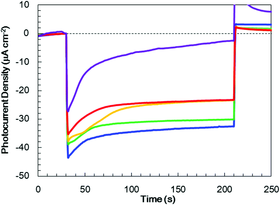 | ||
| Fig. 6 Photocurrent transients for Pt/TiO2/Cr2O3 specimens with various TiO2 layer thicknesses (10 nm; purple line, 30 nm; blue line, 60 nm; green line, 80 nm; yellow line and 120 nm; red line) at +0.11 V vs. RHE in a 0.5 M Na2CO3:NaHCO3 (1:1) buffer electrolyte (pH 9.7) under one sun (100 mW cm−2, AM 1.5) illumination. The thickness of the Cr2O3 layer was fixed at 60 nm. | ||
To investigate the effect of the TiO2 thickness in more detail, incident photon to current conversion efficiency (IPCE) spectra were obtained by irradiation with monochromatic light using band pass filters. Fig. 7 shows the IPCE spectra acquired from Pt/TiO2/Cr2O3 specimens with various TiO2 layer thicknesses. The IPCE spectra of the electrodes with more than 30 nm thick TiO2 layers increased in intensity at 400 nm, showing a good correlation with the absorption spectrum of Cr2O3 (Fig. 4, blue line). Although the IPCE values at wavelengths longer than 340 nm were similar for each electrode, the IPCE values below this point became smaller as the TiO2 layer thickness exceeded 30 nm. These results suggest that light absorption by Cr2O3 was inhibited by the TiO2 overlayer. As an example, as shown by the black line in the absorption spectrum in Fig. 4, a TiO2 layer having a thickness of 60 nm had an absorbance greater than 1 below 320 nm. Thus, more than 90% of the light below this wavelength could not reach Cr2O3. The observation that the IPCE spectra were affected by the TiO2 thickness clearly indicates that the cathodic photocurrent originated from the photoexcitation of Cr2O3, and that light absorption by TiO2 decreased the photocurrent. However, the IPCE values for the photoelectrode with a 10 nm-thick TiO2 layer were lower than those of the other electrodes at almost all wavelengths. Although a 10 nm-thick TiO2 layer covered the surface of Cr2O3 (Fig. S5†), the thickness of TiO2 may be insufficient for the formation of a p–n junction structure. As a result of the trade-off between the light filtering effect of TiO2 and the formation of a charge separation structure, the optimal TiO2 film thickness with regard to generating a large photocurrent is believed to be 30 nm.
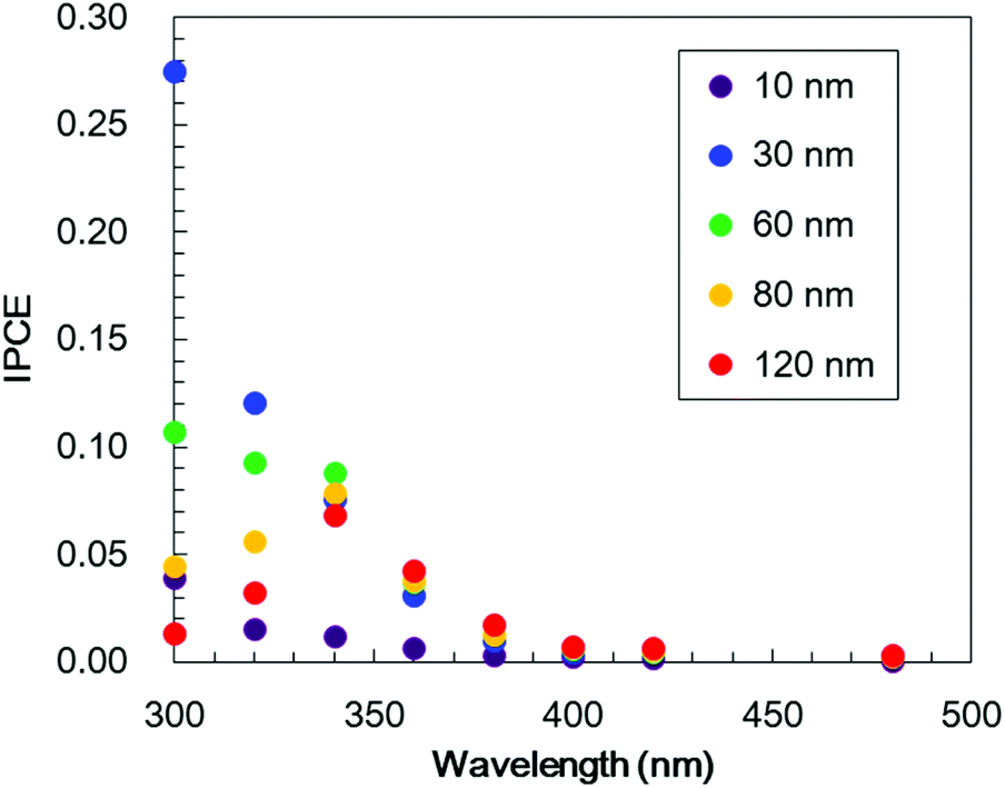 | ||
| Fig. 7 IPCE spectra obtained from Pt/TiO2/Cr2O3 electrodes at various wavelengths using different TiO2 layer thicknesses (10 nm; purple, 30 nm; blue, 60 nm; green, 80 nm; yellow and 120 nm; red) at +0.11 V vs. RHE in a 0.5 M Na2CO3:NaHCO3 (1:1) buffer electrolyte (pH 9.7) under monochromatic illumination. The thickness of the Cr2O3 layer was fixed at 60 nm. | ||
PEC water splitting
To confirm PEC H2 evolution, the gaseous products were analysed by gas chromatography after 1 h of irradiation with AM 1.5 light while applying a bias of +0.11 V vs. RHE (Table 1). The Pt/TiO2(60 nm)/Cr2O3 specimen generated a stable photocurrent over this time span (Fig. S6†), with a charge flow of 110 mC cm−2. During this trial, 510 nmol cm−2 of H2 was produced (entry 1 in Table 1), equivalent to 89% faradaic efficiency. Control experiments without Pt or without both Pt and TiO2 did not produce H2 (entries 2 and 4, Table 1), while a test without TiO2 gave only a very small amount of this product (entry 3 in Table 1). Thus, even if light is absorbed by Cr2O3, PEC water splitting does not proceed without TiO2 and Pt. Therefore, it is considered that PEC water splitting progresses due to the generation of photoexcited electrons in Cr2O3 in response to light absorption. These electrons are transferred to the Pt via the TiO2 charge-separation layer.Conclusion
The generation of H2via solar PEC water-splitting by Cr2O3 was successfully realized following surface modification of the oxide. Bare Cr2O3 was found to produce a significant dark current but a minimal photocurrent. The addition of Pt further deteriorated the performance of this material. Therefore, neither bare Cr2O3 nor Pt/Cr2O3 provided H2 by PEC water-splitting. Applying a TiO2 overlayer with subsequent Pt deposition to fabricate a Pt/TiO2/Cr2O3 electrode resulted in an enhanced photocurrent and realized solar PEC H2 generation. The dark current almost disappeared following this surface treatment, suggesting that TiO2 passivated the Cr2O3 surface. In this layered electrode, a photocathode current was induced in response to light absorption by Cr2O3, while the TiO2 layer acted as a filter to inhibit this light absorption. Nevertheless, since the photocurrent was enhanced by the presence of a TiO2 coating, it is evident that TiO2 also acted as a charge separation layer. Thus, within the Pt/TiO2/Cr2O3 electrode, TiO2 accumulated photoexcited electrons generated by light absorption by Cr2O3 while blocking undesired interactions between Cr2O3 and Pt. As a result, H2 generation was realized through water-splitting. In future, the use of this TiO2 layering technique with a doped Cr2O3 could lead to practical visible-light-driven PEC water-splitting systems.Experimental section
Materials
Tin(IV) oxide/ITO double-layered TCO coated glass (Geomatec Co., Ltd) was used as substrates for the preparation of the electrodes. Commercially available Cr, TiO2 and Pt sputtering targets and TiO2 powder were obtained from the Kojundo Chemical Laboratory Co. A reference sample of Cr2O3 for the XPS analysis and UV/Visible diffuse reflectance spectroscopy was obtained from Nacalai Tesque, Inc.Preparation
A Cr2O3 film was deposited by RF reactive magnetron sputtering of a Cr target with an Ar/O2 (9:1 v/v) plasma. After deposition, the electrodes were annealed at 823 K under an N2/O2 (4:1 v/v) gas flow for 2 h. Subsequently, a TiO2 layer was deposited on the surface of the Cr2O3 thin film by RF reactive magnetron sputtering of a TiO2 target with an Ar/O2 (4:1 v/v) plasma. The deposited electrodes were then annealed at 823 K under an O2 gas flow for 2 h. The Pt cocatalyst was loaded onto either TiO2-coated or bare Cr2O3 specimens by RF magnetron sputtering. The amount of Pt applied was adjusted to obtain an average thickness of 1 nm.
Characterization
The crystal structures of the films were analysed using XRD (Ultima IV, Rigaku Co.) with Cu Kα radiation, while the optical properties of the films were assessed by using UV/visible absorption spectroscopy (UV-3600, Shimadzu Co.). STEM together with EDX was performed using a JEM-2100F microscope (JEOL Co.). Samples for these observations were cut using a focused ion beam (FIB; NB5000, Hitachi High-Tech Co.). Prior to cutting the samples, the film surfaces were coated with carbon and Pt layers to protect the specimens from the FIB. XPS data were acquired using a PHI5000 VersaProbe (Ulvac-Phi Co.) spectrometer.PEC measurements
The photocurrent density measurements were performed in a three-electrode configuration consisting of a silver–silver chloride (Ag/AgCl) electrode, a platinum wire electrode and a prepared photocathode as the working, reference and counter electrodes, respectively. In these trials, the exposed TCO layer of the photocathode was covered with silicone rubber and all potentials were converted to the RHE reference scale using the equation E (vs. RHE) = E (vs. Ag/AgCl) + 0.20 V + 0.059 V × pH. A sealed Pyrex® glass cell was employed as the reactor and Ar-saturated aqueous 0.5 M NaHCO3:Na2CO3 (1:1; pH 9.7) solutions were employed as the electrolytes. An electrochemical analyser (ALS612E and ALSCHI-614C, ALS Co., Ltd) supplied the potential and frequency to the electrode. The electrode was irradiated with a light intensity equivalent to one sun (AM 1.5; 100 mW cm−2) using a solar simulator (HAL-320, Asahi Spectra Co.). Prior to exposure, the light intensity was adjusted with a CS-20 instrument (Asahi Spectra Co.). The sample irradiation was limited to an area of 10 × 10 mm via a slit. Linear sweep voltammetry was conducted at a scan rate of 50 mV s−1 under chopped light irradiation. The photocurrent densities in the photocurrent transient curves were converted by subtracting the dark current density values determined just prior to photo-irradiation from the current densities. The PEC water-splitting reaction, in conjunction with the application of an electrical bias, was conducted while measuring the photocurrent generated under continuous irradiation at a fixed electrode potential of −0.5 V vs. Ag/AgCl. After incubation for 30 min to allow the gaseous reaction products to equilibrate between the liquid and gas phases, these products were analysed by gas chromatography (GC-2014, Shimadzu Co.), employing a thermal conductivity detector and an active carbon column (Shincarbon ST, Shinwa Chemical Industries Co.) with Ar as the carrier gas. IPCE spectra were acquired under monochromatic light generated by a 300 W xenon lamp (MAX-303, Asahi Spectra Co.), using band-pass filters to obtain specific wavelengths.
Conflicts of interest
There are no conflicts to declare.Acknowledgements
The authors wish to thank Ms. Hiroko Uchiyama for technical support.Notes and references
- G. Glenk and S. Reichelstein, Nat. Energy, 2019, 4, 216–222 CrossRef CAS.
- D. Parra, L. Valverde, F. J. Pino and M. K. Patel, Renewable Sustainable Energy Rev., 2019, 101, 279–294 CrossRef CAS.
- I. Staffell, D. Scamman, A. V. Abad, P. Balcombe, P. E. Dodds, P. Ekins, N. Shah and K. R. Ward, Energy Environ. Sci., 2019, 12, 463–491 RSC.
- T. Yao, X. An, H. Han, J. Q. Chen and C. Li, Adv. Energy Mater., 2018, 8, 1800210 CrossRef.
- C. Jiang, S. J. A. Moniz, A. Wang, T. Zhang and J. Tang, Chem. Soc. Rev., 2017, 46, 4645–4660 RSC.
- J. W. Ager, M. R. Shaner, K. A. Walczak, I. D. Sharp and S. Ardo, Energy Environ. Sci., 2015, 8, 2811–2824 RSC.
- A. Fujishima and K. Honda, Nature, 1972, 238, 37–38 CrossRef CAS PubMed.
- A. Kudo and Y. Miseki, Chem. Soc. Rev., 2009, 38, 253–278 RSC.
- R. Abe, J. Photochem. Photobiol., C, 2010, 11, 179–209 CrossRef CAS.
- X. B. Chen, S. H. Shen, L. J. Guo and S. S. Mao, Chem. Rev., 2010, 110, 6503–6570 CrossRef CAS PubMed.
- K. Maeda and K. Domen, J. Phys. Chem. Lett., 2010, 1, 2655–2661 CrossRef CAS.
- K. Maeda, J. Photochem. Photobiol., C, 2011, 12, 237–268 CrossRef CAS.
- F. E. Osterloh, Chem. Soc. Rev., 2013, 42, 2294–2320 RSC.
- T. Hisatomi, J. Kubota and K. Domen, Chem. Soc. Rev., 2014, 43, 7520–7535 RSC.
- A. Miyoshi, S. Nishioka and K. Maeda, Chem. – Eur. J., 2018, 24, 18204–18219 CrossRef CAS PubMed.
- Y. Miseki and K. Sayama, Adv. Energy Mater., 2019, 9, 1801294 CrossRef.
- T. Morikawa, S. Sato, K. Sekizawa, T. Arai and T. M. Suzuki, ChemSusChem, 2019, 12, 1807–1824 CrossRef CAS PubMed.
- H. Yoneyama, H. Sakamoto and H. Tamura, Electrochim. Acta, 1975, 20, 341–345 CrossRef CAS.
- K. Ohashi, J. McCann and J. O. M. Bockris, Nature, 1977, 266, 610–611 CrossRef CAS.
- J. E. Turner, M. Hendewerk, J. Parmeter, D. Neiman and G. A. Somorjai, J. Electrochem. Soc., 1984, 131, 1777–1783 CrossRef CAS.
- M. S. Prévot and K. Sivula, J. Phys. Chem. C, 2013, 117, 17879–17893 CrossRef.
- K. Zhang, M. Ma, P. Li, D. H. Wang and J. H. Park, Adv. Energy Mater., 2016, 6, 1600602 CrossRef.
- A. Liu, H. Zhu and Y.-Y. Noh, Mater. Sci. Eng., R, 2019, 135, 85–100 CrossRef.
- Z. Wang, P. K. Nayak, J. A. Caraveo-Frescas and H. N. Alshareef, Adv. Mater., 2016, 28, 3831–3892 CrossRef CAS PubMed.
- A. Paracchino, V. Laporte, K. Sivula, M. Gratzel and E. Thimsen, Nat. Mater., 2011, 10, 456–461 CrossRef CAS PubMed.
- S. N. F. M. Nasir, M. K. N. Yahya, N. W. M. Sapian, N. A. Ludin, M. A. Ibrahim, K. Sopian and M. A. M. Teridi, RSC Adv., 2016, 6, 56885–56891 RSC.
- S. Ida, K. Yamada, T. Matsunaga, H. Hagiwara, Y. Matsumoto and T. Ishihara, J. Am. Chem. Soc., 2010, 132, 17343–17345 CrossRef CAS PubMed.
- K. Sekizawa, T. Nonaka, T. Arai and T. Morikawa, ACS Appl. Mater. Interfaces, 2014, 6, 10969–10973 CrossRef CAS PubMed.
- T. Morikawa, T. Arai and T. Motohiro, Appl. Phys. Express, 2013, 6, 041201 CrossRef.
- A. Holt and P. Kofstad, Solid State Ionics, 1997, 100, 201–209 CrossRef CAS.
- H. Cao, X. Qiu, Y. Liang, M. Zhao and Q. Zhu, Appl. Phys. Lett., 2006, 88, 241112 CrossRef.
- L. W. Finger and R. M. Hazen, J. Appl. Phys., 1980, 51, 5362–5367 CrossRef CAS.
- L. Pauling and S. B. Hendricks, J. Am. Chem. Soc., 1925, 47, 781–790 CrossRef CAS.
- A. Holt and P. Kofstad, Solid State Ionics, 1999, 117, 21–25 CrossRef CAS.
- S. C. Tsai, A. M. Huntz and C. Dolin, Mater. Sci. Eng., A, 1996, 212, 6–13 CrossRef.
- A. Holt and P. Kofstad, Solid State Ionics, 1994, 69, 127–136 CrossRef CAS.
- B. Medasani, M. L. Sushko, K. M. Rosso, D. K. Schreiber and S. M. Bruemmer, J. Phys. Chem. C, 2018, 122, 12984–12993 CrossRef CAS.
- F. Lebreau, M. M. Islam, B. Diawara and P. Marcus, J. Phys. Chem. C, 2014, 118, 18133–18145 CrossRef CAS.
- K. Sekizawa, K. Oh-ishi, K. Kataoka, T. Arai, T. M. Suzuki and T. Morikawa, J. Mater. Chem. A, 2017, 5, 6483–6493 RSC.
- M. T. Greiner, M. G. Helander, W.-M. Tang, Z.-B. Wang, J. Qiu and Z.-H. Lu, Nat. Mater., 2012, 11, 76–81 CrossRef CAS PubMed.
- Y. Xu and M. A. A. Schoonen, Am. Mineral., 2000, 85, 543–556 CrossRef CAS.
- L. Farrell, K. Fleischer, D. Caffrey, D. Mullarkey, E. Norton and I. V. Shvets, Phys. Rev. B: Condens. Matter Mater. Phys., 2015, 91, 125202 CrossRef.
- E. Arca, K. Fleischer and I. V. Shvets, Appl. Phys. Lett., 2011, 99, 111910 CrossRef.
- H. Wang, Y. Zhang, L. Zhang, Y. Guo, S. Liu, F. Gao, Y. Han, G. Feng, X. Liang and L. Ge, RSC Adv., 2016, 6, 84871–84881 RSC.
- S. Goel, A. Kumar, J. K. Quamara and J. Kumar, Adv. Sci. Lett., 2014, 20, 1562–1566 CrossRef.
- J. J. Carey, M. Legesse and M. Nolan, J. Phys. Chem. C, 2016, 120, 19160–19174 CrossRef CAS.
- E. Arca, K. Fleischer, S. A. Krasnikov and I. Shvets, J. Phys. Chem. C, 2013, 117, 21901–21907 CrossRef CAS.
- D. Bae, B. Seger, P. C. K. Vesborg, O. Hansen and I. Chorkendorff, Chem. Soc. Rev., 2017, 46, 1933–1954 RSC.
- N. Guijarro, M. S. Prevot and K. Sivula, Phys. Chem. Chem. Phys., 2015, 17, 15655–15674 RSC.
- B. Xu, L. Tian, A. S. Etman, J. Sun and H. Tian, Nano Energy, 2019, 55, 59–64 CrossRef CAS.
- M. C. Biesinger, B. P. Payne, A. P. Grosvenor, L. W. M. Lau, A. R. Gerson and R. S. C. Smart, Appl. Surf. Sci., 2011, 257, 2717–2730 CrossRef CAS.
- R. Cheng, B. Xu, C. N. Borca, A. Sokolov, C.-S. Yang, L. Yuan, S.-H. Liou, B. Doudin and P. A. Dowben, Appl. Phys. Lett., 2001, 79, 3122–3124 CrossRef CAS.
- M. M. Abdullah, F. M. Rajab and S. M. Al-Abbas, AIP Adv., 2014, 4, 027121 CrossRef.
- C.-S. Cheng, H. Gomi and H. Sakata, Phys. Status Solidi A, 1996, 155, 417–425 CrossRef CAS.
- R. Cohen, L. Kronik, A. Shanzer, D. Cahen, A. Liu, Y. Rosenwaks, J. K. Lorenz and A. B. Ellis, J. Am. Chem. Soc., 1999, 121, 10545–10553 CrossRef CAS.
- Y. Li, L. Zhang, W. Wu, P. Dai, X. Yu, M. Wu and G. Li, Nanoscale Res. Lett., 2014, 9, 270 CrossRef PubMed.
Footnote |
| † Electronic supplementary information (ESI) available: An image of the crystal structure, UV/visible absorption spectra, STEM-EDX images and PEC properties. See DOI: 10.1039/C9DT04296B |
| This journal is © The Royal Society of Chemistry 2020 |