
 Open Access Article
 This Open Access Article is licensed under a
 Creative Commons Attribution 3.0 Unported Licence
Molecular materials as interfacial layers and additives in perovskite solar cells
Maria
Vasilopoulou
 *a,
Azhar
Fakharuddin
b,
Athanassios G.
Coutsolelos
c,
Polycarpos
Falaras
a,
Panagiotis
Argitis
a,
Abd. Rashid bin Mohd
Yusoff
d and
Mohammad Khaja
Nazeeruddin
*e
*a,
Azhar
Fakharuddin
b,
Athanassios G.
Coutsolelos
c,
Polycarpos
Falaras
a,
Panagiotis
Argitis
a,
Abd. Rashid bin Mohd
Yusoff
d and
Mohammad Khaja
Nazeeruddin
*e
aInstitute of Nanoscience and Nanotechnology, National Center for Scientific Research “Demokritos”, 15341 Agia Paraskevi, Attica, Greece. E-mail: m.vasilopoulou@inn.demokritos.gr
bDepartment of Physics, University of Konstanz, D-78464, Konstanz, Germany
cDepartment of Chemistry, University of Crete, Laboratory of Bioinorganic Chemistry, Voutes Campus, Heraklion 70013, Crete, Greece
dDepartment of Physics, Swansea University, Vivian Tower, Singleton Park, SA2 8PP, Swansea, UK
eInstitute of Chemical Sciences and Engineering, École Polytechnique Fédérale de Lausanne (EPFL), Rue de l’Industrie 17, CH-1951 Sion, Switzerland. E-mail: mdkhaja.nazeeruddin@epfl.ch
First published on 4th June 2020
Abstract
Solar cells based on organo-metal halide perovskites have gained unprecedented research interest over the last few years due to their low-cost solution processability, high power conversion efficiency, which has recently reached a certified value of 25.2%, and abundance of raw materials. Nevertheless, the best efficiencies remain below the Shockley–Queisser theoretical limit of 32.5% due to several losses arising from either defect traps present in the bulk of the perovskite absorber or at the device heterointerfaces. While bulk defects are detrimental for the device performance by mainly limiting the open circuit voltage, interfacial layers are also crucial. They dictate the charge transfer/transport from the perovskite layer to the collecting electrodes, hence influencing the device photocurrent, but also act as protective barriers against oxygen and moisture penetration. Molecular materials and additives are widely used to improve the bulk properties of perovskite absorbers through the formation of high-quality perovskite films with superior optoelectronic properties, and improved crystallinity, and also of electronically clean interfaces with minimum losses during charge transfer/transport. In this review, we analyze the predominant pathways that contribute to voltage and current losses due to poor interfaces and also due to non-radiative recombination losses arising from inferior perovskite morphology and its inherent polycrystalline and highly defective nature. We then discuss strategies for achieving interfacial organic and inorganic molecular materials for application as electron and hole transport layers in perovskite solar cells with ideal energy levels, high charge mobilities and improved thermal, photo, and structural stability. Moreover, the prerequisites for molecular additives to achieve dimensionality engineering, defect passivation, molecular cross-linking, interfacial energy alignment and electronic doping are thoroughly discussed. Finally, we examine prospects for future research directions and commercialization.
 Maria Vasilopoulou | Dr Maria Vasilopoulou received her degree in Physics from the University of Athens and her PhD in Functional Materials for Nanolithography from the School of Chemical Engineering of the National Technical University of Athens. Then she worked, as a postdoctoral researcher, at the National Center for Scientific Research Demokritos (NCSRD) where she developed organic and inorganic materials for application as interfacial layers in organic solar cells and light emitting diodes. She is currently a senior Researcher at the Institute of Nanoscience and Nanotechnology of NCSRD. Her research activity focuses on the area of organic and halide perovskite optoelectronic devices and mainly on organic/organic and organic/inorganic interface characterization. She has published more than 100 scientific papers in international journals and conference proceedings and holds five patents. |
 Azhar Fakharuddin | Azhar Fakharuddin obtained a PhD in Advanced Materials from University Malaysia Pahang where he worked on improving the charge collection efficiency in dye-sensitized solar cells. He then joined the University of Konstanz, Germany, as an Alexander von Humboldt Research Fellow to work on ‘interfaces and processes in perovskite/organic solar cells’. He subsequently moved to IMEC, Belgium to work on perovskite LEDs. His current research focuses on novel materials and processes for high efficiency optoelectronic devices, mainly solar cells and light emitting diodes and their related device physics. |
 Abd. Rashid bin Mohd Yusoff | Dr Abd. Rashid Mohd Yusoff obtained his BSc in Physics from Universiti Putra Malaysia in 2002. In 2011, he completed his PhD working with the late Prof. Ivo Hümmelgen's group in the Departamento de Física at Universidade Federal do Paraná, Brazil. Dr Mohd Yusoff's doctoral research focused on magnetic-field effects in semiconducting materials and devices. From 2011 to 2013 he was a Postdoc Fellow working with Prof. Jin Jang at the Department of Information Display, Kyung Hee University. He then worked as a Research Professor in the same group until 2018, which was when he joined the Sêr SAM group at Swansea University. Dr Mohd Yusoff is a Senior Research Fellow with Sêr SAM with a focus on perovskite photovoltaics. His research interests include photovoltaics, light emitting diodes, transistors, photochemical water splitting, and bifunctional electrocatalysts. |
 Mohammad Khaja Nazeeruddin | Prof. Mohammad K. Nazeeruddin's current research at EPFL focuses on perovskites and and light-emitting diodes. He has published more than 700 peer-reviewed papers, and ten book chapters, and is an inventor/co-inventor of over 75 patents. He has been named a Thomson Reuters “Highly Cited Researcher” since 2014, and one of the 19 scientists identified by Thomson Reuters as The World's Most Influential Scientific Minds from all scientific domains. He has been identified by the Times Higher Education as one of “the top 10 researchers in the world working on high impact perovskite materials and devices”. (https://www.timeshighereducation.com/data-bites/top-universities-and-researchers-perovskite-solar-cell-research#survey-answer). He was appointed as a World Class University (WCU) professor and Adjunct Professor at King Abdulaziz University, Jeddah, and elected to the European Academy of Sciences (EURASC), and is a Fellow of The Royal Society of Chemistry. http://gmf.epfl.ch/. |
Introduction
Solar cells based on organo-metal halide perovskites are considered as an attractive alternative to silicon-based photovoltaics as they can be produced at a lower cost even on flexible substrates using widely available low temperature deposition techniques. The focus of the research community working on solar cells has mainly been concentrated on perovskite materials of the general formula ABX3, where A is a monovalent cation such as methyl ammonium (MA), formamidinium (FA), caesium (Cs), and rubidium (Rb); B is a heavy metal such as lead (Pb) and tin (Sn); and X refers to a halogen anion (i.e. Cl, Br, and I).1–5 Such a complex composition of the perovskite absorber often leads to a distorted, defect-rich bulk structure and a complex surface chemical composition with consequences for the device operation.6–11 Although certified power conversion efficiencies (PCEs) of up to 25.2% (for research cells) and 16.1% (for modules) have been recently demonstrated by employing novel materials and advancements in cell architectures, reproducibility and stability concerns hamper their further development and use in commercial products.In practical applications, a perovskite solar cell (PSC) behaves like a current generator under light illumination, delivering a photo-current density the larger part of which flows to the load delivering the measured short-circuit current density (Jsc). However, the existence of large series resistance (Rs) contributes to a large reduction in the device Jsc. The resistance of the bulk perovskite layer and the electrodes and the interfacial contact resistance due to large energy mismatch or poor physical quality of the perovskite and the electrodes synergistically contribute to the measured device Rs. Furthermore, the attainment of a high voltage output under open circuit conditions (Voc) is a prerequisite in achieving optimum device performance. The limitations in Voc are mainly imposed by non-radiative recombination losses within the absorber bulk and at the absorber/electrode heterointerfaces. Improvements in Voc require finding ways to restrict the recombination channels.
However, even in state-of-the-art PSCs, there exist significant non-radiative losses mainly originating from ionic defect states such as organic cation (i.e. MA+ and FA+) and halide (I− and Br−) vacancies present in the perovskite absorber, which limit further improvement in the device PCE.12–14 The presence of non-radiative recombination centres derived from defects located on the perovskite surface or at its grain boundaries also has a detrimental effect on the device stability as they induce several degradation processes in the perovskite layer.15,16 To approach the Shockley–Queisser (SQ) efficiency limit and to simultaneously enhance the device long-term stability, all non-radiative recombination losses inside PSCs should be suppressed, whereas their quantum yield should be maximized, approaching unity.17
In this regard, several methodologies for the defect passivation and molecular cross-linking of grains have been applied as effective strategies to manipulate trap states, hence boosting simultaneously the device efficiency and stability. Additionally, as these cells are fabricated with thin perovskite films incorporated between two electrode contacts, the role of the various cell interfaces is of paramount importance for achieving optimal cell performance metrics such as efficiency and stability. To improve these interfaces, charge transport interlayers with suitable electronic and physical properties are inserted between the absorber layer and the collecting electrodes. These are the hole transport layer (HTL) and the electron transport layer (ETL), defined by their charge selectivity and collection efficiency.18–20 Efficient charge collection leads to ideal current–voltage behaviour and maximized PCE. Therefore, a wide variety of interfacial engineering strategies have been demonstrated to circumvent major interfacial issues such as energetic alignment, charge transfer, charge accumulation, recombination and extraction. This manuscript reviews the recent literature on the design and synthesis of novel molecular materials for application as morphology manipulators, electronic dopants and trap passivation agents for the perovskite absorber and its heterointerfaces and as charge transport interlayers in high efficiency PSCs. In particular, Section 1 includes a short discussion on the basic principles governing the optical and electronic properties of perovskite absorbers. We next continue by reviewing recent developments on molecular materials used to engineering the hole transport interface (Section 2), which was the PSC component first subjected to intense research (the electron transport interface was generally based on mesoporous or compact TiO2). In Section 3, we review recent progress on the design and synthesis of molecular materials as additives to improve the main device component, the perovskite absorber. Section 4 summarizes developments on molecular materials to engineer the electron selective interface. Section 5 includes a summary and perspectives.
1. Organo-metal halide perovskites
Perovskites are an extraordinary class of materials ideally comprised of a cubic cell with ABX3 stoichiometry. The A-site is occupied by a monovalent cation, usually organic, such as MA+ and FA+, and the B-site by a divalent cation such as Pb2+ and Sn2+, whereas the X-site is occupied by a monovalent halide anion (I−, Br−, and Cl−).21 The smaller charge on the X site of halide perovskites compared to the established oxide ones decreases the ionic character of the bonds, hence decreasing Coulomb interactions, and, therefore, plays a key role in the optoelectronic properties of these materials.22,23 The ionic radii of both cations and ions determine the dimensionality of the perovskite material, which can range from the Ruddlesden–Popper phase (R2An−1BnX3n+1), that is, it has a 2D or quasi-2D perovskite structure, to true 3D perovskites.24 Perovskites with different dimensionalities have strikingly different properties including long carrier-diffusion lengths, high optical-absorption coefficients and tolerance for intrinsic defects, which are all key factors governing the device performance.25,26The electronic band structure of perovskites determines their unique optical and electronic properties such as long carrier lifetime, intense absorption within the visible spectrum and adequate hole and electron mobilities. For the AXB3 perovskites consisting of [PbI6]4− octahedra, the valence band (VB) is mainly composed of Pb 6s–I 5p σ-antibonding orbitals, while the conduction band (CB) is formed by the mixing of Pb 6p–I 5p π-antibonding and Pb 6p–I 5s σ-antibonding orbitals. The elemental contributions to each band depend on the perovskite stoichiometry. This can serve as guidance to design and develop novel perovskite materials with advanced optoelectronic properties. In general, to support superior PSC performance and stability we need high optical absorption coefficients (of the order of 105 cm−1) to absorb more light in thin films, long carrier lifetimes to extend the carrier diffusion length and minimized recombination losses and well-balanced charge transport within the perovskite towards the collecting electrodes.27
To ensure the latter, PSCs based on existing perovskites, which have not yet reached the superior properties foreseen for the ideal cubic materials, usually comprise a perovskite absorber sandwiched between a hole (p) and electron (n) transport/extraction layer and are classified into three major configurations: mesoporous n–i–p with a mesoscopic layer, regular planar n–i–p and inverted planar p–i–n. The defect-tolerant nature of perovskites is of paramount importance because it generates high Voc.28 As in most kinds of existing solar cells (with the exception of GaAs single-junction solar cells), PSCs undergo a large thermal loss in Voc with respect to their bandgap energy (Eg). Such a voltage loss is often one-third of Eg and contributes to a significant loss of the PCE. Again, the material complexity, despite the large tolerance factor, is mirrored in the defect-rich nature of the bulk perovskites and surfaces (Fig. 1a).29 Passivation of such defects through the anchoring of appropriate functional groups or molecules within the perovskite lattice and surface (Fig. 1b) could eliminate losses in Voc. The heterointerfaces with the adjacent hole/electron transport layers are also crucial since they largely affect the device performance and stability due to poor energetic alignment at these interfaces and surface trap state population and chemical reaction induced degradation of the absorber with its neighbouring layers. With these inherent perovskite bulk material and surface and perovskite/electrode interface characteristics in mind, we herein review the most notable examples of specific developments in molecular materials that successfully overcome these problems in halide perovskite solar cells.
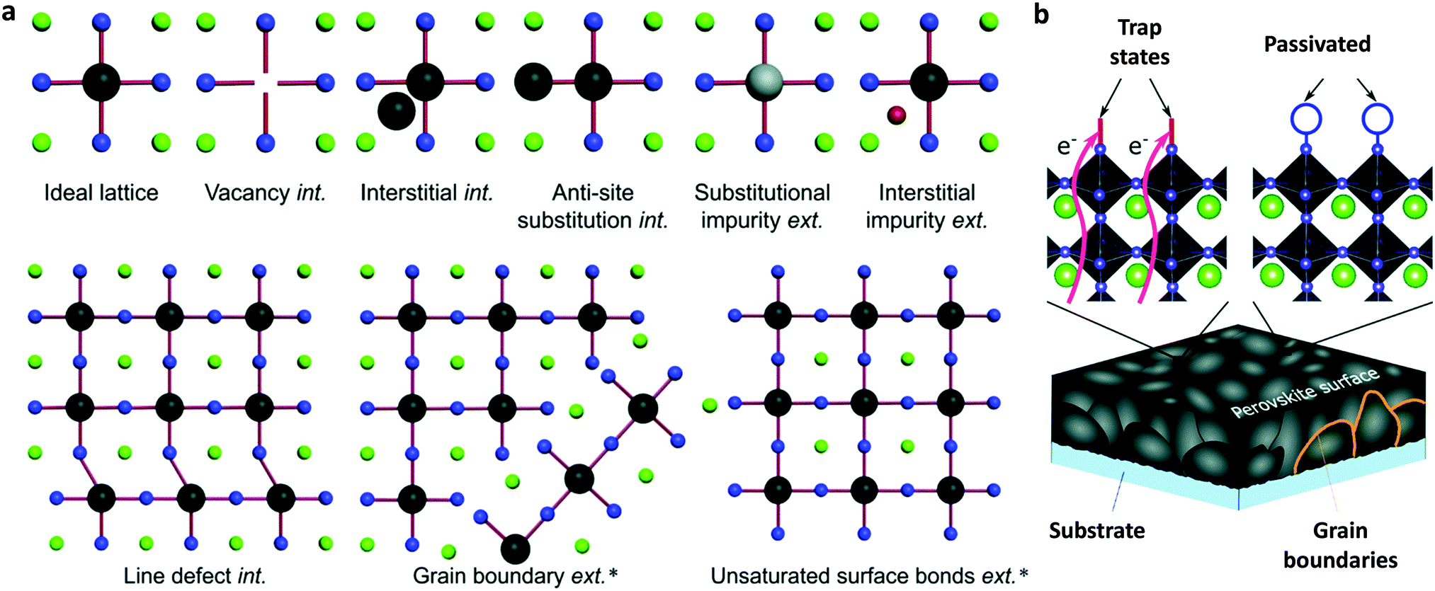 | ||
| Fig. 1 (a) Illustration of the intrinsic (int.) and extrinsic (ext.) defects present in lead halide perovskites compared to an ideal lattice. The asterisk denotes those that have been identified experimentally. (b) Schematic representation of surface trap states and their passivation by introducing additional atoms or molecules (denoted with blue circles) which bind to improperly bound orbitals which cause the trap states. The green, black and blue spheres represent A, B and X elements, respectively, while the grey and red represent different impurities. This figure has been adapted from ref. 29 with permission from The Royal Society of Chemistry, Copyright 2020. | ||
2. Molecular materials as hole transport layers in perovskite solar cells
Generally, the PSC architecture includes five individual layers, namely the anode electrode, the hole transport/extraction layer (HTL/HEL), the perovskite absorber, the electron transport/extraction layer (ETL/EEL) and the cathode contact.30 The device efficiency and stability highly depend on the implementation of suitable charge transport layers as they dictate the photogenerated charge extraction towards the respective electrodes and charge transfer/accumulation at the interfaces, and also act as physical barriers to avoid direct contact between the perovskite absorber and the anode/cathode electrodes. As perovskite materials are ambipolar charge-conductors, they produce nearly free negative and positive charges; the positive charges should be transported through the perovskite and then through the HTL to the respective electrode (cathode), while the negative charges should be blocked from reaching the cathode. Therefore, the HTL plays a key role in enhancing the device efficiency through effectively transferring holes and blocking electrons in both the regular (n–i–p) and inverted (p–i–n) architectures.There are several criteria that efficient HTLs should fulfill such as suitable energy level alignment with the perovskite, that is, to have their valence band maximum (VBM) or highest occupied molecular orbital (HOMO) nearly aligned or slightly deeper than the VBM of the perovskite material in order to facilitate efficient hole transfer; to have their conduction band minimum (CBM) or lowest unoccupied molecular orbital (LUMO) higher than the perovskite CBM to successfully block the photogenerated electrons from reaching the opposite electrode; to possess high hole mobilities, hence allowing fast charge transport; to present increased thermal, chemical and photochemical stability and mobility to contribute to prolonged lifetime of the fabricated device; and to exhibit low cost preparation and processing methods.31–36 For HTLs implemented in the inverted p-i-n structure, the refractive index and the extinction coefficient should also be taken into consideration because the HTL should also allow maximum light intensity to reach the perovskite absorber. Moreover, they must be processed from orthogonal solvents relative to the polar ones used for the preparation of the perovskite precursor solution in order to resist solvation during PSC fabrication. Finally, these layers are also important in modifying the morphology/crystallization of the perovskite overlayer in the inverted structure, which significantly influences the device efficiency and, importantly, stability.37–40
The majority of the hole transport materials (HTMs) employed in PSCs include p-type polymer semiconductors, inorganic metal oxides, and semiconducting molecular materials, either organic such as small molecules and oligomers or inorganic such as metal selenides, tellurides, sulphides etc. Solution-processed polymer semiconductors (which can also be considered as large molecules) and molecular materials (of smaller molecular weight compared to polymers) requiring low temperature for their preparation are promising for application in flexible devices. There are several recent reviews summarizing the pros and cons of p-type polymer semiconductors and inorganic metal oxides used as efficient hole transport materials in PSCs.41–44 To the authors knowledge, there are no reports in the recent literature on the classification of smaller molecular materials of both types of organic and inorganic ones and application as either hole or electron transport materials in PSCs. Therefore, in this review, we place the emphasis on the successful application of the well-established organic and the recently emerged inorganic molecular materials as charge transport interlayers which facilitate low-cost device fabrication. Especially, the inorganic ones show the potential to highly elongate the device stability due to their robustness and resilience to environmental moisture, although at the expense of high performance.45–47 They also possess the advantage of simple preparation processes compared to inorganic metal oxides, which usually require high-temperature sintering after deposition.
In the next sections, we will highlight design guidelines and synthetic routes and implemented strategies and approaches for modifying the hole selective device interface with a large variety of smaller molecular materials, which are summarized as follows: small molecules, oligomers, porphyrins and phthalocyanines, and inorganic molecular materials (i.e. polyoxometalates, CuSCN, CuI, etc.). We also include a brief report on the recent developments of polymer semiconductors as HTMs as they can also be considered as large molecules.
2.1 Small molecules
Small molecules have been successfully incorporated as HTLs in PSCs to enhance the photovoltaic performance metrics. Following appropriate design rules, they can be tuned to match the energy alignment of their HOMO level with the VBM of the perovskite absorber to minimize losses during charge transfer and hence maximize the device Voc. In addition, their high hole mobility and high conductivity also contribute to achieving a high fill factor (FF). Furthermore, their solubility in organic solvents and the overall good thermal and photochemical stability enhance the device operational lifespan. Besides their extensive use as hole transport materials (HTMs), they have also been applied as surface modifiers in PSCs with an inverted (p–i–n) architecture as they modify the work function (WF) of the underlying cathode, resulting in strengthening of the device built-in field and hence accelerating hole extraction. In the same PSC architecture, they can also alter the surface energy of the underlayer, hence causing beneficial modification in the nanomorphology of the perovskite absorber coated on top of them. Their insertion as HTLs in regular (n–i–p) PSCs has also been proven to be beneficial to the device stability because they protect the photoactive layer from moisture ingression and oxygen penetration.The most commonly used organic small molecule hole transport material is spiro-OMeTAD (2,2′,7,7′-tetrakis-(N,N-di-4-methoxy-phenylamino)-9,9′-spirobifluorene), which was first used by Bach et al. in 1998 in dye-sensitized solar cells (DSSCs).48 However, as it shows low conductivity (∼10−5 S cm−1) spiro-OMeTAD requires the addition of dopants. Burschka et al. used a 2.2% doping ratio of tris[2-(1H-pyrazol-1-yl)pyridine] cobalt(III) tris(hexafluorophosphate) (FK102) and obtained an increase in PCE from 2.3% (reference device) to 5.6% (doped).49 Hagfeldt and colleagues used a 0.03% ratio of the dopant (tris(2-(1H-pyrazol1-yl)-4-tert-butylpyridine) cobalt(III) tri[bis(trifluoromethane)sulfonimide]) (FK209) to demonstrate mixed cation PSCs with a remarkable PCE of 20.1%.50,51 Luo et al. hence introduced the use of Li-TFSI along with t-BP to dope spiro-OMeTAD,52–55 which inhibited the charge carrier recombination and allowed for a PCE of 14.32%. They also compared their results with those obtained through doping of spiro-OMeTAD with 1.5 mol% F4-TCNQ. In this case, the PCE reached a value of 12.93%, but the device's stability and reproducibility were far better when compared to cobalt complexes as dopants.
Several modifications of the chemical structure of spiro-OMeTAD have also been attempted. In fact, the large variety of small molecules used as HTLs in PSCs is based on spiro-OMeTAD molecular modification. They mainly targeted a change in the oxidation potential, and an increase in the conductivity of the pristine molecule. In such an attempt, Jeon and colleagues synthesized three different molecules, where the –OMe group was in the ortho, para or meta position (po-spiro-OMeTAD, pp-spiro-OMeTAD, and pm-spiro-OMeTAD, respectively), aiming to investigate the steric effect on the oxidation potential of these materials.56 These modifications allowed for the achievement of higher FF values compared to the pp-spiro-OMeTAD molecule and, consequently, a higher PCE up to 16.7%. Moreover, the position of the methoxy groups was found to critically affect the resilience of spiro-OMeTAD against degradation. Shifting of the methoxy groups from the para to the meta position gave rise to compounds such as spiro-m-OMe, spiro-3,5-OMe, spiro-p-tBu, spiro-3,5-tBu, spiro-3,5-mixed, spiro-OMe-TPA and spiro-p-OHex, which were found to be more robust.57 Further molecular modification approaches included the replacement of these groups with ethyl and thiomethyl ones.58–61
Grätzel et al. designed and used a novel transport material (spiro-CPDT, X59) with a 4,4′-spirobi[cyclopenta[2,1-b:3,4-b′]dithio-phene] core and triarylamine terminal units (Fig. 2a).60 This material exhibited comparable hole mobility and conductivity to spiro-OMeTAD. As a result, PSCs based on X59 as the HTL exhibited similar PCE values (up to 19.8%) to that of the reference device using spiro-OMeTAD. Moreover, the optimized devices employing X59 as the HTL (Fig. 2b) exhibited minimized hysteresis (Fig. 2c), excellent reproducibility and reasonable stability under dark conditions (Fig. 2d). The stability of X59 was superior compared to the reference device with spiro-OMeTAD and it had an additional advantage of low-cost preparation of the HTM. Moreover, the incorporation of fluorine moieties has recently arisen as an effective approach to synthesize advanced spiro-based HTLs with superior optical and electronic properties.62–65 Saliba and co-workers designed a dissymmetric fluorene–dithiophene molecule (FDT) as a low-cost alternative to spiro-OMeTAD.63 This small molecule based-PSC yielded a conversion efficiency of 20.1%. Similarly, a spiro-based HTL, the donor–acceptor–donor (D–A–D) type spiro[fluorene-9,9′-phenanthren-10′-one]-core small molecule called Yih-2, delivered improved PSC performance,65 and was also more resistant to moisture in ambient conditions compared to conventional spiro-based materials, leading to better long-term device stability. The most successful examples of this category, however, are fluorene-terminated HTMs, such as DM (N2,N2′,N7,N7′-tetrakis(9,9-dimethyl-9H-fluoren-2-yl)-N2,N2′,N7,N7′-tetrakis(4-methoxyphenyl)-9,9′-spirobi[fluorene]-2,2′,7,7′ tetraamine), developed by Jeon and co-workers.66 The fabricated PSCs using the newly synthesized materials (DM) achieved record efficiencies up to 23.2% due to the fine-tuned energy levels. The devices with DM materials also showed better thermal stability than the device with spiro-OMeTAD, showing 95% of their initial performance for more than 500![[thin space (1/6-em)]](https://www.rsc.org/images/entities/char_2009.gif) h at 60°C.
h at 60°C.
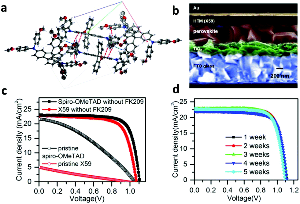 | ||
| Fig. 2 (a) Illustration of the stacking modes of molecules of X59 within the b axis. (b) Scanning electron microscopy (SEM) cross-sectional image of the PSC using the small molecule X59 as the HTL. (c) Current density–voltage (J–V) characteristic curves of PSCs based on X59 and spiro-OMeTAD HTLs for comparison. (d) Stability test of the device with X59. This figure has been adapted from ref. 60 with permission from Elsevier, copyright 2016. | ||
Spiro-OMeTAD is well-known to degrade due to oxidation and efforts to completely replace it as the HTM are reported. In such a report, Zhang et al. introduced a new strategy to design dopant-free hole transport materials that include charged moieties and counter ions (Fig. 3a).51 The tail end of the alkyl chains present in the non-optimized material (AS37) has initially been modified by attaching tertiary amine groups (X41). In a more optimized version (X44), two quaternary ammonium ions were coupled with associated counter ions TFSI−. The device based on this ionic HTM X44 (Fig. 3b) and with no additional doping showed an impressive PCE of 16.2% (Fig. 3c). This high performance was attributed to the increased hole conductivity and the homogeneity of the formed HTM thin film. This work provided design rules and paved the way for the synthesis of novel small molecules for use as HTMs for PSCs.
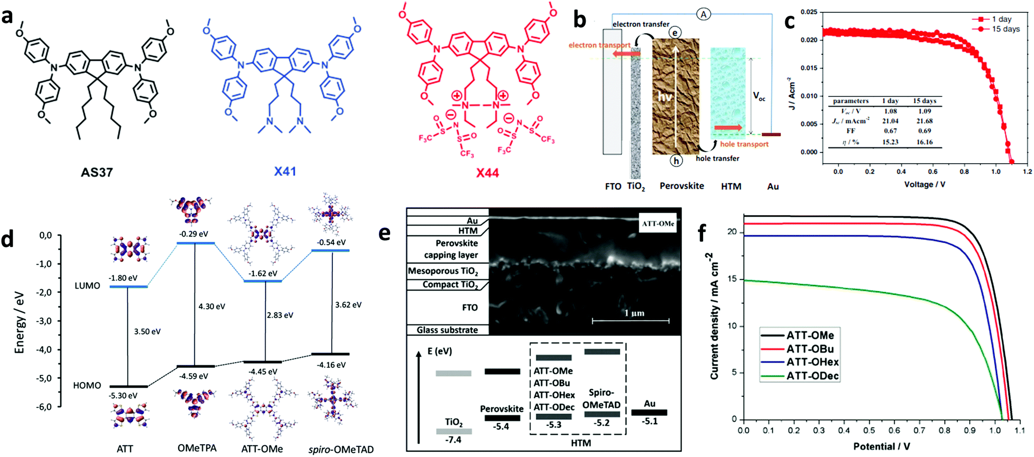 | ||
| Fig. 3 (a) Chemical structures of HTMs: AS37, X41, and X44. (b) Pathways of interfacial charge transfer and charge transport in the perovskite solar cells, and (c) J–V characteristic curves of the best performing device with X44. This figure has been adapted from ref. 51 with permission from John Wiley and Sons, Copyright 2017. (d) Energy diagram showing the frontier molecular orbitals computed for the ATT, OMeTPA, ATT-OMe, and spiro-OMeTAD compounds. (e) Cross-section SEM image of the different layers of a PSC (top), and the energy diagram of the different device layers (bottom). (f) J–V characteristic curves of the devices with different HTMs. This figure has been adapted from ref. 69 with permission from John Wiley and Sons, Copyright 2017. | ||
In order to avoid the multistep and expensive synthesis of spiro-MeOTAD, other small molecules have been synthesized and employed as HTLs in PSCs, such as thiophene, triphenylamine, triazatruxene, and carbazole derivatives.67–80 In addition to being low-cost alternative HTLs, these materials were designed with the aim of combining appropriate optical and electronic properties and higher resistance to oxidation compared to spiro-OMeTAD.
Among the newly synthesized compounds, those based on thiophenes have delivered the most promising results. Sun et al. synthesized a thiophene derivative, namely 2,6,14-tris(5′-(N,N-bis(4-methoxyphenyl)aminophenol-4-yl)-3,4-ethylenedioxy-thiophen-2-yl)-triptycene (TET), whose production cost was unexpectedly low and optoelectronic properties were far superior.67 Its application in planar PSCs yielded a PCE of 19.10%, while its cost was cut down to 20% of conventional spiro-based HTLs. In another study, Zimmermann and co-workers created small molecules based on an anthra[1,2-b:4,3-b′:5,6-b′′:8,7-b′′′]-tetrathiophene (ATT) core, named ATT-OMe, ATT-OBu and ATT-OHex (Fig. 3d),69 where the methoxy groups on the triarylamine sites were replaced by butoxy-and hexoxy-groups showing improved solubility. The employed small molecule HTLs exhibited energetic positions dependent on their molecular structure. The fabricated PSCs (Fig. 3e) exhibited PCEs of 18.10%, 17.30%, and 15.70%, respectively (Fig. 3f); the perovskite PL quenching demonstrated that this was due to facilitated hole transfer. This work clearly demonstrated the potential of ATT derivatives to successfully replace spiro-OMeTAD. Furthermore, derivatives exhibiting thiophene cores have also been proven to be beneficial for hole transport.70 García-Benito and co-workers synthesized an isomeric benzotrithiophene (BTT)-cored material crosslinked with p-methoxytriphenylamines, called BTT-4. PSCs based on the BTT-4 HTL, which exhibited good thermal stability up to 430 °C, obtained a high conversion efficiency of 18.97%.71 We note that the conductivity of thiophene based HTMs was enhanced when combined with other derivatives reported above such as truxenes. Such a material combination could serve as a design platform for the future development of more advanced HTMs based on small molecules for PSCs. For instance, modification of materials belonging to two other important families of small molecule HTLs in PSCs, e.g., triazatruxene81–84 and carbazole derivatives, holds great promise.85–88 Upon core modification of triazatruxene-based small molecules, dopant free HTMs, namely KR131 and KR133, were recently obtained.81 PSCs based on those materials delivered PCE values of 17.70% and 15.80%, respectively, attributed to the efficient hole extraction from the perovskite layer towards the cathode. Additionally, molecular modification was also deemed necessary for carbazole-based HTMs. An environmentally friendly HTL termed CzPAF-SBF was recently developed,87 upon introducing peripheral OMeTAD groups outside the carbazole core. Finally, alternative small molecules were also synthesized to serve as effective HTLs in PSCs. For instance, Yussof et al. introduced deoxyribose nucleic acid (DNA)–hexadecyl trimethyl ammonium chloride (CTMA) as an HTL in inverted PSCs, which delivered a PCE value of 15.86%, ascribed to the efficient charge transport of the HTL, while also showing long-time stability under ambient conditions.89 Small molecules used as HTMs are summarized in Table 1 where the type of absorber and the performance metrics of the resultant PSC are also shown. Summarizing the above, small molecules represent the most favorite class of materials applied as HTLs in PSCs. To date, spiro-OMeTAD remains the most promising small molecule due to its appropriate energy levels and adequate hole mobility. However, it presents major drawbacks such as high cost and complex synthesis and the need for external doping with ionic salts and additives that enhance the device performance but limit its stability. Recent advancements made to avoid these drawbacks include the design and synthesis of various organic small molecules consisting of spiro cores linked to xanthene, fluorine, carbazole or thiophene derivatives. Recent developments in small molecule-based HTLs for application in PSCs include a large number of scientific reports.90,91 The authors encourage the reader to refer to an excellent review paper by Urieta-Mora et al., entitled “Hole transporting materials for perovskite solar cells: a chemical approach”.92
| Small molecule | PSC absorber | PCE (%) | J sc (mA cm−2) | V oc (V) | FF | Ref. |
|---|---|---|---|---|---|---|
| F4-TCNQ | MAPbI3 | 12.9 | 19.04 | 0.93 | 0.73 | 53 |
| LiTFSI + tBP-spiro-OMeTAD | MAPbI3 | 14.3 | 20.57 | 1.00 | 0.7 | 53 |
| pm-Spiro-OMeTAD | MAPbI3 | 13.9 | 21.10 | 1.01 | 0.65 | 55 |
| po-Spiro-OMeTAD | MAPbI3 | 16.7 | 21.20 | 1.02 | 0.78 | 55 |
| pp-Spiro-OMeTAD | MAPbI3 | 20.0 | 20.70 | 1.00 | 0.71 | 55 |
| X59 | FA0.85MA0.15Pb(I0.85Br0.15)3 | 19.8 | 23.40 | 0.73 | 0.73 | 59 |
| FDT | MAPbBr3 | 20.2 | 22.70 | 1.15 | 0.76 | 62 |
| Yih-2 | MAPbBr3 | 16.1 | 22.18 | 1.02 | 0.71 | 64 |
| DM | (FAPbI3)0.95(MAPbBr3)0.05 | 22.3 | 24.80 | 1.11 | 0.81 | 65 |
| As37 | (FAPbI3)0.95(MAPbBr3)0.05 | 7.8 | 20.05 | 1.06 | 0.37 | 66 |
| X44 | MAPbX3 | 15.2 | 21.04 | 1.06 | 0.66 | 66 |
| TET | MAFAPbI3 | 19.1 | 21.96 | 1.07 | 0.81 | 67 |
| ATT-ome | (FAPbI3)0.85(MAPbBr3)0.15 | 18.3 | 21.75 | 1.07 | 0.78 | 69 |
| BTT-4 | (FAPbI3)0.85(MAPbBr3)0.15 | 18.9 | 23.04 | 1.09 | 0.75 | 71 |
| CzPAF-SBF | MAPbI3 | 20.7 | 23.09 | 1.10 | 0.81 | 87 |
| DNA-CTMA | MAPbI3 | 15.9 | 20.85 | 1.04 | 0.73 | 89 |
2.2 Oligomers
In addition to the aforementioned organic small molecules, novel low bandgap π-oligomers (OLs) have been recently exploited as HTLs in PSCs. The most successful examples are 3D oligomers and those using the donor–acceptor (D–A) or acceptor–donor–acceptor (A–D–A) molecular architecture, which enables more efficient charge transfer, hence improving the device performance. Some of the first successful results were the 3D oligomers X54 and X55 consisting of a spiro[fluorene-9,9′-xanthene] (SFX) core developed by Xu et al.93 In particular, X55 showed a marvelous 3D structure due to its bulky SFX units, excellent stability and a PCE of 20.8% when used as a HTL in PSCs. Sun and co-workers developed a HTL based on benzodithiophene linked via phenoxazine-bridges and end-capped with 3-ethylrhodanine (OL-1).94 The undoped material was inserted as the bottom HTL in inverted PSCs, which achieved maximum PCEs of 13.2%, representing a significant improvement compared to the reference devices based on spiro-OMeTAD. Other examples of 3D oligomers used as efficient HTMs in PSCs include heteroacenes which contained either thiophenes or pyrroles in their molecular structure. Gratzel and co-workers reported the development of a thiophene–pyrrole oligomer with asymmetrical structure containing different thiophene spacers and end-capped with dicyanovinylene acceptor units (OL-2 and OL-3).95 Conventional mesoporous MAPbI3-based devices with those oligomers used as undoped-HTLs reached 10.5% and 9.5%, respectively. Later, the same group developed two novel S,N-heteropentacene-based HTLs which had their central scaffold flanked by either ethylenedioxythiophene (EDOT) or thiophene units, and end-capped with a dicyanovinylene acceptor (OL-4 and OL-5).96Non-doped OL-4 and OL-5 were incorporated in mesoscopic PSCs, yielding a maximum PCE of 11.24% and 10.04%, respectively. In another study, a benzodithiophene (BDT) based derivative (OL-6) having BDT linked with alkylated thiophene–benzothiadiazole spacers was developed for application in mesoscopic PSCs, which displayed a PCE of 13.4%.97 Appending pyridine moieties as end-caps onto the BDT central scaffold, the same authors later presented novel oligomer-based HTLs (OL-7, OL-8 and OL-9) with the aim of studying the influence of different counter ions (Br− and TFSI−) on the performance of PSCs.98 They found that the ionic materials displayed faster charge transfer rates and higher hole mobilities. When employed as additive-free HTLs in mesoscopic PSCs, these HTLs result in a remarkable average PCE of 17.4%, which was slightly lower than that of the control device using doped spiro-OMeTAD (17.9%). This work initiated the interest in oligomers bearing appropriate counter anions to advance their effectiveness as HTMs in PSCs.
Furthermore, D–A and A–D–A oligomers have been of particular interest. Yang and co-workers developed A–D–A systems using a thienosilole as a π-bridge between electron-accepting rhodamines and a central core consisting of either an electron-donating alkylthienyl-substituted benzo[1,2-b:4,5-b′]dithiophene (OL-10) or an electron-withdrawing 5,6-difluoro-2,1,3-benzothiadiazole (OL-11).99 Whereas OL-9 based devices achieved an improvement in PCE up to 16.2%, OL-10 based devices showed poor performance (a PCE of 6.2%), which was ascribed to poor carrier mobility of the HTL. Later, Gratzel and co-workers designed and developed donor–bridge–acceptor (D–B–A) systems for application as HTLs in PSCs.100 In those oligomers, the D unit was an engineered TPA, whereas the A unit was a dicyanovinylene moiety. The B group was an S,N-heteropentacene (OL-12). Conventional mesoporous PSCs with LiTFSI and t-BP doped OL-11 as the HTL yielded a maximum PCE of 16.9% using 1,1′,2,2′-tetrachloroethane as the processing solvent. Later, the same group further enhanced the performance metrics of their PSCs up to 17.7% using HTLs based on these D–B–A systems by molecular engineering of the donor moiety and length increasing of the π-conjugated S,N-heteroacene bridge.101 The structures of oligomers OL-1 to OL-12 are shown in Fig. 4, while the performance metrics of representative PSCs using those oligomers as HTMs are listed in Table 2. Overall, conjugated oligomers are highly promising for application as HTLs in PSCs as they exhibit the advantages of low-cost synthesis and ease of modification of their structures. However, they are generally inferior to spiro-OMeTAD based small molecules due to their poor hole mobilities. Advancements can be made through the incorporation of appropriate counter ions within their structure to increase their mobilities and charge transport properties.
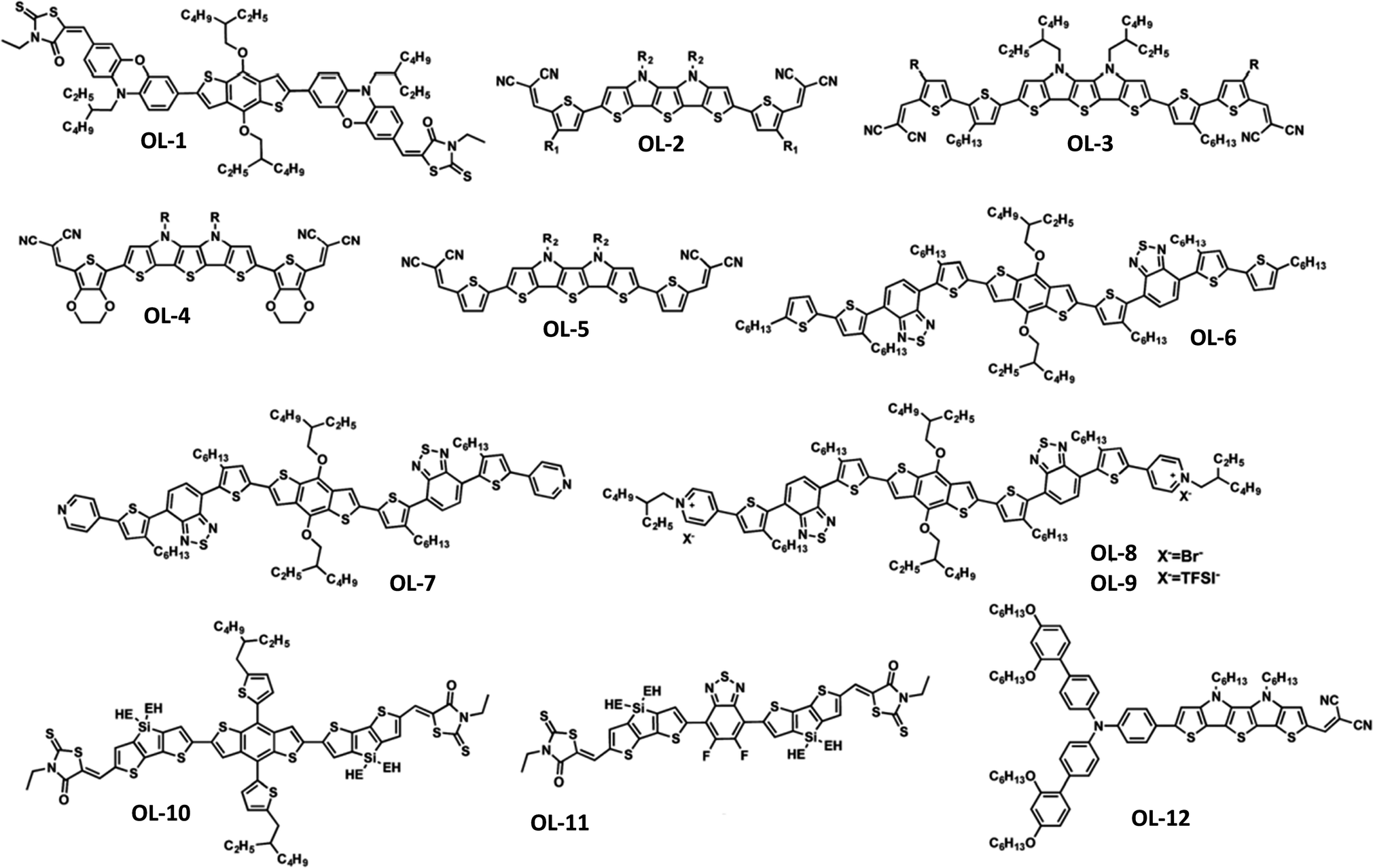 | ||
| Fig. 4 Molecular structures of p-conjugated oligomers as HTMs. This figure was reproduced from ref. 92 with permission from The Royal Society of Chemistry, Copyright 2018. | ||
| Oligomer | PSC absorber | PCE (%) | J sc (mA cm−2) | V oc (V) | FF | Ref. |
|---|---|---|---|---|---|---|
| OL-1 | MAPbI3 | 13.1 | 18.80 | 1.03 | 0.68 | 94 |
| OL-2 | MAPbI3 | 10.5 | 16.40 | 0.99 | 0.65 | 95 |
| OL-3 | MAPbI3 | 9.5 | 15.20 | 0.90 | 0.68 | 95 |
| OL-4 | MAPbI3 | 11.2 | 16.50 | 0.95 | 0.72 | 96 |
| OL-5 | MAPbI3 | 10.0 | 15.84 | 0.90 | 0.70 | 96 |
| OL-6 | MAPbI3 | 13.9 | 18.40 | 1.00 | 0.76 | 98 |
| OL-7 | (FAPbI3)0.85(MAPbBr3)0.15 | 13.0 | 19.83 | 1.04 | 0.63 | 98 |
| OL-8 | (FAPbI3)0.85(MAPbBr3)0.15 | 15.1 | 21.94 | 1.05 | 0.66 | 98 |
| OL-9 | (FAPbI3)0.85(MAPbBr3)0.15 | 17.4 | 22.84 | 1.10 | 0.69 | 98 |
| OL-10 | MAPbI3−xClx | 16.2 | 21.20 | 1.05 | 0.73 | 99 |
| OL-11 | MAPbI3−xClx | 6.2 | 17.10 | 0.98 | 0.37 | 99 |
| OL-12 | (FAPbI3)0.85(MAPbBr3)0.15 | 16.9 | 22.20 | 1.05 | 0.73 | 100 |
2.3 Porphyrins and phthalocyanines
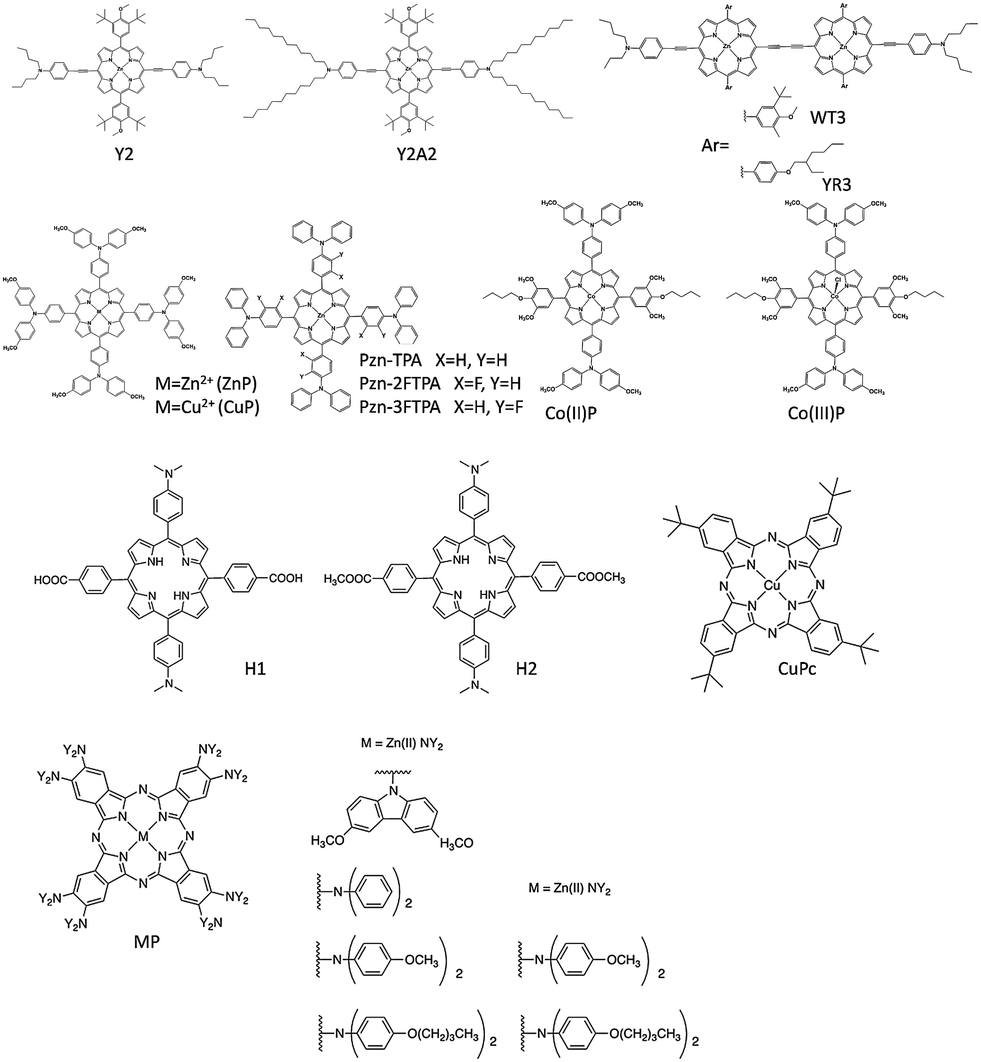
Inspired by natural photosynthesis, porphyrins, phthalocyanines and their analogues have been extensively investigated as molecular absorbers and charge transfer mediators in several classes of optoelectronic devices. Their synthetic versatility offers many possibilities to design and develop novel porphyrin (P) and phthalocyanine (Pc) compounds for solar cell applications. Furthermore, they present excellent thermal and photochemical stability and optical and electronic properties that can be easily adjusted through modification of their structure. As a consequence, they are expected to play a prominent role when employed as charge transport components in several classes of photovoltaic devices.Porphyrins exhibit the significant advantage of being solution-processed in many types of polar and non-polar solvent. To allow for efficient hole transport, they have been mainly used in regular PSCs in the form of single layers (pristine and doped) deposited on top of the perovskite absorber. In 2016, the first report on the application of porphyrin-based HTLs in PSCs was published.102 Two symmetrical porphyrins referred to by the authors as Y2 and Y2A2 featuring a meso 5,15-bis(ethynylaniline) structure with alkoxyphenyl groups at opposite sides of the molecules were reported. The HOMO levels of these compounds were −5.25 and −5.10 eV for Y2 and Y2A2, respectively, in close similarity to the HOMO level of the most common HTL in PSCs, namely spiro-OMeTAD (−5.22 eV). The PCE values of PSCs employing these HTLs between the perovskite absorber and the cathode electrode were 16.60% for Y2, and 10.55% for Y2A2. Although these values were lower than that of the reference device with spiro-OMeTAD (18.03%), the porphyrin-modified devices were proven to have better stability and moisture resistance compared to the reference one.
Subsequently, dimeric porphyrin conjugates based on Y2 (YR3 and WT3) were synthesized.103 The PSC with compound WT3 as the HTL showed a remarkable PCE of 19.44% and improved moisture and thermal stability compared to the reference device spiro-OMeTAD. The application of the symmetric porphyrins ZnP and CuP as HTLs in PSCs was also reported.104 Such porphyrins can be easily synthesized with direct pyrrole condensation with the appropriate benzaldehyde. The devices having these compounds as HTLs presented inferior performance compared to the reference one. However, the main advantage of these materials was their improved stability compared to spiro-OMeTAD used in the reference device. These porphyrins were later modified with side groups, whereas fluorine atoms were also incorporated within their structure.105 PSCs with the fluorinated PZn-2FTPA and PZn-3FTPA showed increased charge injection/transfer and better hole transport compared to the non-fluorinated porphyrin PZn-TPA counterparts. PSCs employing doped PZn-2FTPA HTLs achieved the highest PCE of 18.85%, while the PZn-3FTPA and PZn-TPA based devices showed modest PCE values of 17.71 and 16.37%, respectively.106 Recently, a remarkable record PCE of 20.5% was reported by Tang and co-workers upon the application of HTLs using a mixture of two porphyrins Co(II)P and Co(III)P (Fig. 5a and b).107 Sinapoyl malate was used at the interface of TiO2 and the perovskite in order to improve the UV stability and the contact between the two phases. The device obtained an efficiency of 20.5%, which was higher than a control device employing spiro-OMeTAD (Fig. 5c and d). Moreover, these devices exhibited better reproducibility and higher stability compared to the reference PSCs based on spiro-OMeTAD. Besides metallated compounds, two A2B2 type free base porphyrins have been synthesized by Coutsolelos et al., to be used as the HTL in PSCs.108 Although the devices based on these compounds (H1 and H2) showed inferior performance as compared to a control device using spiro-OMeTAD, this work paved the way for the application of metal free porphyrins as HTLs in PSCs.
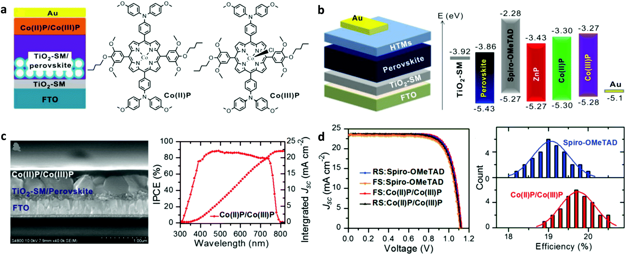 | ||
| Fig. 5 (a) Schematic illustration of the mesoporous PSCs and chemical structures of Co(II)/Co(III) porphyrins used as HTMs. (b) The planar device architecture and the energy level alignment. (c) Cross-sectional SEM image of a planar PSC device and the corresponding internal-photon-to-electron-conversion efficiency (IPCE), and (d) best J–V data and histograms of cell efficiencies among 30 cells with spiro-OMeTAD and Co-porphyrins as HTMs. This figure was adapted from ref. 107 with permission from John Wiley and Sons, Copyright 2018. | ||
Similarly, phthalocyanines have also been successfully applied as the HTL in PSCs, either in the form of single-layers (pristine or doped) or implemented as a multi-junction HTL. They present a large number of advantages including versatility, thermal and chemical robustness and low preparation cost. They can be either solution-processed or vacuum deposited. In this review, we focus on representative examples of solution-processed phthalocyanines only as HTLs in PSCs. For more information regarding the application of both vacuum deposited and solution-processed compounds as hole transport materials in PSCs, the authors refer the reader to a comprehensive recent review by Urbani et al.109
Substituted b-tetrapropyl Cu-phthalocyanine (Cu-3) was the first successful example of the application of a solution-processed dopant-free phthalocyanine HTL in PSCs.110 A maximum PCE of 17.8% and excellent stability were achieved with this HTL, which was found to exhibit a face-on orientation on the perovskite absorber. Later, several papers reported the implementation of solution-processed Pc compounds as HTMs in PSCs.111–115 Seo et al. introduced the application of tert-butyl copper(II) phthalocyanine (CuPc, Fig. 6) as a dopant in a molecularly engineered spiro-OMeTAD (po-spiro-OMeTAD) as the HTL in formamidinium lead iodide based PSCs.111 A device efficiency of up to 19.4% was obtained, due primarily to a significant enhancement in the device FF. Kim et al. focused on the application of CuPc for thermally stable PSCs.112 Their devices recorded a high PCE of ∼18% and maintained nearly 97% of their initial efficiency for more than 1000 h of thermal annealing at 85 °C as a result of the formation of a strong interfacial and conformal coating present on the surface of the perovskite. Furthermore, two novel metallo-phthalocyanines (MPcs) were recently used by Nazeeruddin et al. as alternative HTLs in PSCs.115 These authors designed and tested a series of symmetric MPcs (M = Zn(II) or Cu(II)) bearing eight diarylamino substituents of diverse type that were attached at the ligand peripheral positions through N–C bonds. The nature of the diarylamino substituents was proven to be a key factor in determining the device performance. The highest PCE of 18.10% was obtained using a ZnPc bearing eight bis(p-butoxyphenyl)amino substituents. The chemical structures of porphyrins and phthalocyanines used as HTMs in PSCs are summarized in Fig. 6. These results provide an important future direction for the development of suitable materials for highly efficient and thermally stable PSCs. Porphyrins and phthalocyanines are excellent candidates because, although they have shown inferior performance when used as HTLs in PSCs compared to spiro-OMeTAD, they, however, achieved remarkable stabilities. Furthermore, they present facile, low-cost synthesis and ease of molecular modifications to achieve properties that are beneficial for the device performance.
 | ||
| Fig. 6 Chemical structures of representative examples of porphyrins and phthalocyanines used as HTLs in PSCs. | ||
2.4 Conjugated polymers
Conjugated polymers are different from molecular materials in terms of molecular weight. However, the focus of this review is on the application of smaller weight molecular materials in PSCs. Nevertheless, because conjugated polymers can be viewed as large molecules we include in this review a brief discussion, while also referring the reader to relevant review papers focusing on such materials.43,116Many classes of conjugated polymers were successfully applied to fabricate solution-processed, stable, cost effective and high efficiency PSCs.117–129 Most examples include poly(3-hexylthiophene) (P3HT), poly (3,4-ethylenedioxythiphene):poly(styrenesulfonate) (PEDOT:PSS), (poly-[[9-(1-octylnonyl)-9H-carbazole-2,7 diyl]-2,5-thiophenediyl-2,1,3-benzothiadiazole4,7-diyl-2,5-thiophenediyl]) (PCDTBT), poly[2,1,3-benzothiadiazole-4,7-diyl[4,4-bis(2-ethylhexyl)-4H-cyclopenta[2,1-b:3,4-b′]dithio-phene-2,6-diyl]] (PCPDTBT), and poly-triarylamine (PTAA).
Ulfa et al. applied P3HT as the HTM in PSCs and compared it with spiro-OMeTAD.124 They also used LiTFSI and tBP additives to achieve better device performance. The additives had a profound impact mainly in the case of spiro-OMeTAD. They limited the charge recombination at the interface, reduced the interfacial defects and favored the hole transfer from the perovskite to the HTM layer. Importantly, they found that the P3HT conductivity is not the main limiting parameter of the cell efficiency due to the intrinsic conducting properties of the thiophene chain.
Most inverted devices employ PEDOT:PSS as the bottom HTL.127,128 However, PEDOT:PSS corrodes the ITO bottom electrode, hence causing migration of indium into PEDOT:PSS. Furthermore, the highly hygroscopic nature of PEDOT:PSS makes it prone to degrade the device due to water uptake. To address these drawbacks, Zhao et al. used an alternative p-type polymer, namely poly[N,N′-bis(4-butylphenyl)-N,N′-bis(phenyl)benzidine] (poly-TPD), as the HTL and electron blocking layer for inverted PSCs (Fig. 7).129 They found that the resulting perovskite film deposited through solution-processing on top of poly-TPD consisted of large crystallites with complete coverage on the poly-TPD surface. The average device PCE reached a value of 13.8% and a maximum value as high as 15.3%. It has been thus far shown that polymer semiconductors have great potential for developing low-cost, high-efficiency solar cells using perovskites as light absorbers and these materials as HTLs in either the regular or the inverted architecture.
 | ||
| Fig. 7 (a) The inverted PSC architecture and (b) energy level diagram for PSCs using poly-TPD as the bottom HTL. This figure was adapted from ref. 129 with permission from John Wiley and Sons, Copyright 2015. | ||
2.5 Inorganic molecular hole transport materials
Apart from organic molecular materials, inorganic ones such as molecular polyoxometalates or other novel inorganic semiconducting molecular materials such as copper-based semiconductors, transition metal dichalcogenides and transition metal carbides have been recently employed as HTLs in PSCs. Recent advances concerning the implementation of these materials as interlayers in PSCs are herein discussed with an emphasis on their functionalities and their role in improving the solar cell performance.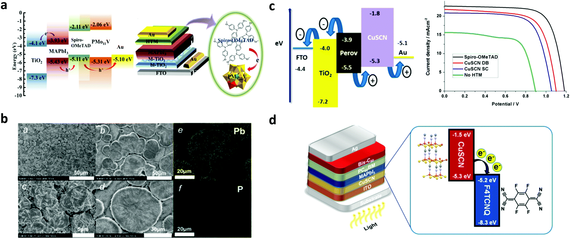 | ||
| Fig. 8 (a) Energy level diagram of the components of PSCs employing a PMo11V POM p-type dopant on a spiro-OMeTAD HTL. Schematic architecture of the fabricated PSCs incorporating the POM doped HTL. This figure was adapted from ref. 130 with permission from American Chemical Society, Copyright 2017. (b) SEM images showing the morphology of the perovskite layer employing a representative PMo11V POM p-type dopant on a spiro-OMeTAD HTL. This figure was adapted from ref. 132 with permission from The Royal Society of Chemistry, Copyright 2017. (c) Energy levels and current density–voltage characteristics for PSCs employing a CuSCN HTL, using either the spin-coating or the doctor-blading technique for preparing different thickness films. This figure was adapted from ref. 137 with permission from American Chemical Society, Copyright 2016. (d) Device structure and energy levels for PSCs using an F4-TCNQ doped CuSCN HTL. This figure was adapted from ref. 138 with permission from The Royal Society of Chemistry, Copyright 2019. | ||
In order to increase its hole conductivity, p-type molecular doping with strong organic electron acceptors such as C60F48 (Fig. 8c),137 and F4-TCNQ (Fig. 8d)138 has been successfully demonstrated. The p-type doped CuSCN layers were employed as HTLs in PSCs. Improved PCEs of 14.40% for p–i–n type/MAPbI3 based PSCs have been reported, accompanied by lower dark current139 and enhanced shunt and lower series resistance compared to the reference device with spiro-OMeTAD. The enhanced solar cell performance was attributed to the enhanced hole mobility and the facile hole transfer as a result of the Fermi level shift towards the valence band of the p-type doped CuSCN, thus reducing the interfacial energetic mismatch.
To exploit synergistically the advantageous effect of another recently emerged molecular inorganic HTL, namely CuI, and CuSCN in enhancing the solar cell performance, solution-processed CuI/CuSCN composite films were proposed as effective HTLs in p–i–n type MAPbI3−xClx based planar PSCs.139 While CuI and CuSCN as HTLs resulted in PCEs of 14.53% and 16.66%, respectively, a significantly enhanced PCE of 18.76% was recorded for the PSCs with the composite HTL. The improved performance of the composite compared to the pristine layers was attributed to the smoother perovskite film quality obtained upon introducing CuSCN as an underlayer for perovskite growth and its higher electrical conductivity. Summarizing the above, inorganic molecular materials applied as HTLs in PSCs are still in their infancy. However, due to their promising characteristics including robustness and resilience to moisture they hold promise for highly stable and efficient devices and are therefore of substantial interest.
3. Molecular materials as additives in perovskite solar cells
An established methodology to simultaneously enhance the performance and stability of PSCs is the inclusion of additives in the perovskite material to alter the resultant film morphology, the density of trap states, the electronic properties etc. These additives usually exhibit large diversity, ranging from molecules to polymers, salts, metals and nanoparticles. The well-established coordination ability of lead cations and iodide anions present in the perovskite matrix represents the stepping stone for building the foundation for this methodology; through the formation of coordination bonds (i.e. hydrogen bond interactions) these additives are incorporated within the perovskite lattice. Among others, molecular additives are advantageous as they are easier to incorporate within the perovskite material and their chemical structure can be widely tuned via facile synthetic procedures. To understand the origin of the coordination bonds between these materials and perovskites it should be taken into account that lead cations are generally considered as a Lewis acid, capable of making coordination bonds with molecular bases, whereas halide anions are treated as Lewis bases, which can coordinate with molecular acids.140 Most molecular additives are introduced into the perovskite precursor solution during its preparation step. However, others are inserted (i.e. spun) into the perovskite surface using their solutions in appropriate solvents through a post-processing step. In most cases, the additives remain in the perovskite material (or its outer surface) after deposition, whilst in a few cases they are removed. In all cases, however, they adopted one or many roles, such as to engineer the perovskite dimensionality, manipulate the film morphology, stabilize some unstable phases, modulate the energy level alignment at the heterointerfaces, and passivate surface and bulk defects, hence suppressing non-radiative recombination losses, eliminating hysteresis and boosting the performance and stability of PSCs. In this review, we summarize recent results and briefly discuss functioning mechanisms and influences of additives on PSCs. A recent review of Liu et al. also summarizes recent developments on the role of additives in FA and Cs containing perovskites.140 Molecular materials used as additives in the perovskite layer are summarized in Table 3.| Additive | Perovskite | PCE (%) | J sc (mA cm−2) | V oc (V) | FF | Ref. |
|---|---|---|---|---|---|---|
| PZPY | Cs0.04MA0.16FA0.8PbI0.85Br0.15 | 18.1 | 21.70 | 1.08 | 0.77 | 143 |
| TAPbI3 | MAFAPbI3 | 19.0 | 22.81 | 1.08 | 0.77 | 144 |
| ITIC-Th | FA0.83Cs0.17Pb(Br0.2I0.8)3 | 19.2 | 22.46 | 1.13 | 0.76 | 155 |
| TBAB | MAPbI3−xClx | 11.7 | 19.20 | 0.90 | 0.68 | 156 |
| Aniline | FAPbI3 | 13.8 | 23.00 | 0.93 | 0.64 | 161 |
| Benzyl amine | FAPbI3 | 17.3 | 23.30 | 1.08 | 0.68 | 161 |
| Phenethylamine | FAPbI3 | 13.3 | 23.60 | 0.95 | 0.59 | 161 |
| IPFB | MAPbX3 | 15.7 | 23.38 | 1.06 | 0.67 | 166 |
| MACl | FAPbI3 | 20.7 | 23.09 | 1.10 | 0.81 | 176 |
| tert-Butylpyridines | MAPbI3 | 17.3 | 22.70 | 1.08 | 0.71 | 187 |
3.1 Perovskite dimensionality engineering
The instability of PSCs remains amongst the most significant reason preventing their mass production. Novel engineering approaches are investigated to address the stability of PSCs, especially against humidity and light soaking. In the relevant literature, there are some reports exploring the concept of inserting hydrophobic species within the bulk or on the surface of the perovskite material to improve the stability of PSCs. Most of the published studies involve the implementation of nitrogen derivatives such as alkylammonium cations,141 phenylalkylamine,142 and pyrazol-yl pyridine compounds.143 These derivatives form coordination bonds with the perovskite material through a rapid exchange of protons, hence stabilizing lower dimension phases of the perovskite. In a relevant example, the authors prepared a 1D–3D hetero-structure in the entire volume of the absorber. Particularly, 2-(1H-pyrazol-1-yl)pyridine (PZPY) was introduced into lead halide 3D perovskites,143 which allows 1D–3D hybrid perovskite materials to be obtained (Fig. 9a and b). The resultant 1D–3D perovskites enabled a remarkably prolonged photoluminescence decay lifetime, hence significantly suppressing carrier recombination compared to the 3D perovskite. The intrinsically stable but able to move 1D material allowed the engineered perovskite system to alleviate the lattice mismatch of the 1D–3D hybrid perovskite (Fig. 9c). It also passivated interfacial traps, thus showing a self-healing ability during the crystal growth process of the 1D–3D perovskite. The PSCs fabricated using these novel 1D–3D perovskites exhibited a higher efficiency and improved long-term stability as compared to the 3D counterpart.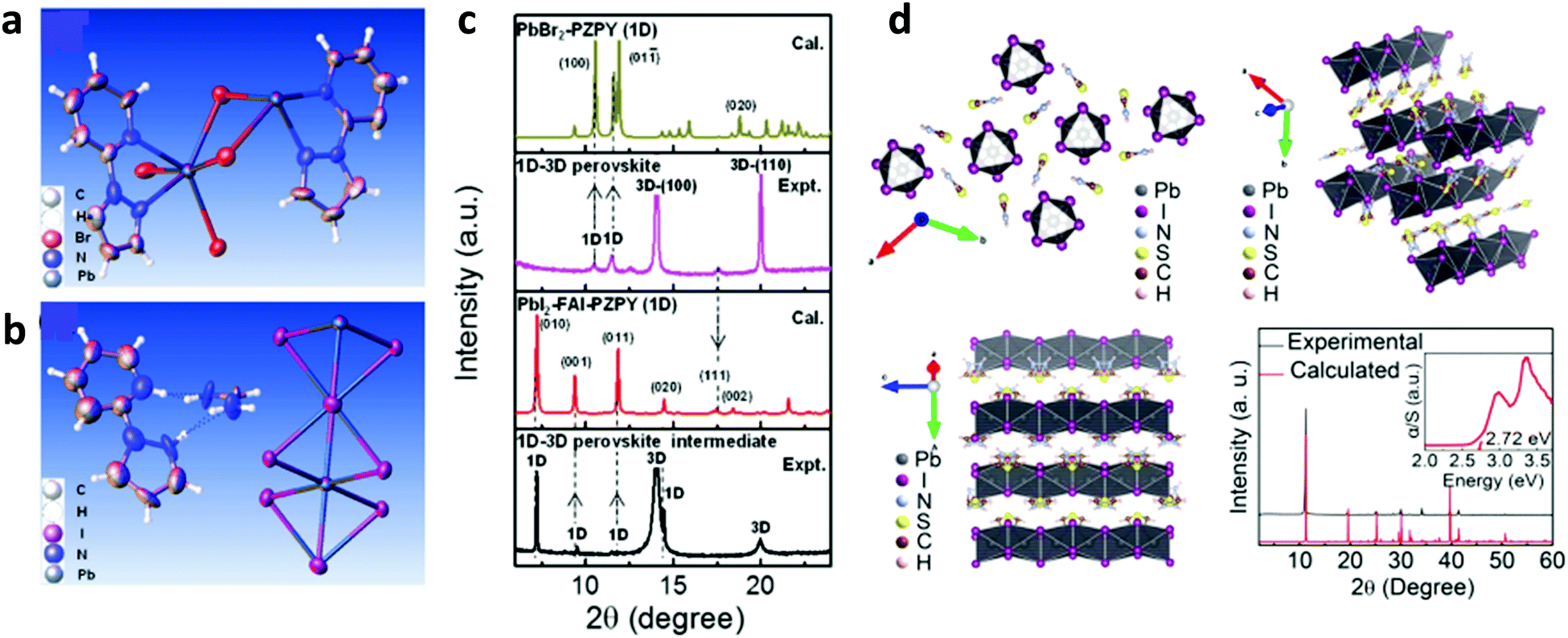 | ||
| Fig. 9 Thermal ellipsoid representation for (a) the lead bromide (PbBr)–PZPY single crystal structure and (b) for the lead iodide (PbI)–formamidinium iodide (FAI)–PZPY crystal structure. (c) X-ray diffraction (XRD) patterns calculated from the structural data of PbBr–PZPY (1D) and PbI–FAI–PZPY (1D) single crystals, and XRD patterns characterizing the 1D–3D perovskite thin film and the corresponding intermediate. This figure was adapted from ref. 143 with permission from John Wiley and Sons, Copyright 2018. (d) Part of the TAI-based 1D perovskitoid structure viewed along different directions (up, left and right, and bottom, left) and comparison of the calculated and as-made PXRD patterns of the TAPbI3 single crystals (bottom, left); inset: optical absorption spectrum showing the absorption edge at 2.72 eV. This figure was adapted from ref. 144 with permission from American Chemical Society, Copyright 2019. | ||
Recently, a 1D perovskite capping layer employing thiazole ammonium iodide having an aromatic character (thiazo ring) and preserving the quaternary ammonium group was proposed for improved stability in PSCs.144 Particularly, the problem of severe instability was solved by using epilayers of a wide-band-gap 1D lead iodide perovskitoid structure, which was based on a short organic cation, namely, thiazole ammonium (TA) in the form of lead iodide (TAPbI3). This 1D capping layer, in addition to passivating the surface of the three dimensional (3D) perovskite film, also promoted charge transport and the charge carrier lifetime. Moreover, it also prevented the migration of iodide anions within the 3D perovskite (Fig. 9d). The corresponding device reached a high maximum PCE of 18.97% while also retaining 92% of this efficiency upon exposure to ambient air for a period of two months. However, it is well known that sulfur based organo-compounds are more hydrophobic than nitrogen ones. In particular, sulfonium-based ionic materials have generated substantial interest in solar cells as potential alternatives to their ammonium counterparts, due to practical benefits including higher chemical and electrochemical stabilities.145–147
In this context, interface optimization was recently proposed148 by adding an air stable wide band-gap 1D perovskite layer based on a tertiary sulfonium compound on top of the main absorber. The additional perovskite (1D) layer creates a favorable environment that improves the performance, reproducibility and stability of the main perovskite absorber (a 3D perovskite). In fact, the devices based on the 3D/1D bilayer show a significant decrease in charge carrier recombination accompanied by improved stability. The surface of the film reacted to form an advantageous 1D perovskite layer which reduced trap states, provided a shield against water molecule ingression and promoted the charge carrier transport in the PV devices. These 3D/1D bilayer PSCs showed higher stability in ambient conditions as well as under continuous light illumination.
3.2 Manipulation of the perovskite layer morphology
The development of materials and methods that improve the quality of the perovskite film remains a hot topic as both the nanomorphology and crystallinity represent key factors influencing the overall device performance. There are several elements affecting the perovskite morphology including the intrinsic properties of the material itself, the choice of deposition method, the existence of impurities, the surface energy of the substrate and the application of post-treatment. Molecular additives are also commonly adopted for achieving beneficial tuning of the perovskite morphology even in large-area perovskite films.Generally, molecular additives influence the perovskite film morphology through altering the colloid distribution in the perovskite precursor.149 The colloidal clusters in the precursor solution act as nucleation centers for growth and crystallization of the perovskite, hence directly modulating the resultant perovskite crystallization and film morphology.150 Both of these have a direct impact on the device performance and stability.151 Molecular additives with acidic nature, such as hydroiodic (HI) and hydrobromic acids (HBr), have been shown to significantly affect the perovskite morphology by causing the dissolution of large perovskite particles to smaller ones but with a more uniform distribution of particles.152 As an example, Heo et al. fabricated dense and uniform perovskite films with higher surface coverage on the substrate by introducing HBr to the precursor solution.153 The introduction of HBr increased the perovskite solubility in DMF, yielding dense films that prolonged the device performance relative to the reference one without the additive (Fig. 10a and b). Apart from acidic additives,154 other types of small molecules were also employed to alter the perovskite morphology. Qin et al. recently used a non-fullerene acceptor, namely (3,9-bis(2-methylene-(3-(1,1-dicyanomethylene)-indanone))-5,5,11,11-tetrakis(5-hexylthienyl)-dithieno[2,3-d:2′,3′-d′]-s-indaceno[1,2-b:5,6-b′] dithiophene) (ITIC-Th), as an additive to the perovskite precursor.155 Characterization suggested that ITIC-Th suppressed the formation of the yellow δ-FAPbI3 phase. Consequently, the devices fabricated from the precursor solution with the ITIC-Th additive serving as a stabilizer (Fig. 10c) exhibited higher performance and overall stability compared with the references without any additive (Fig. 10d).
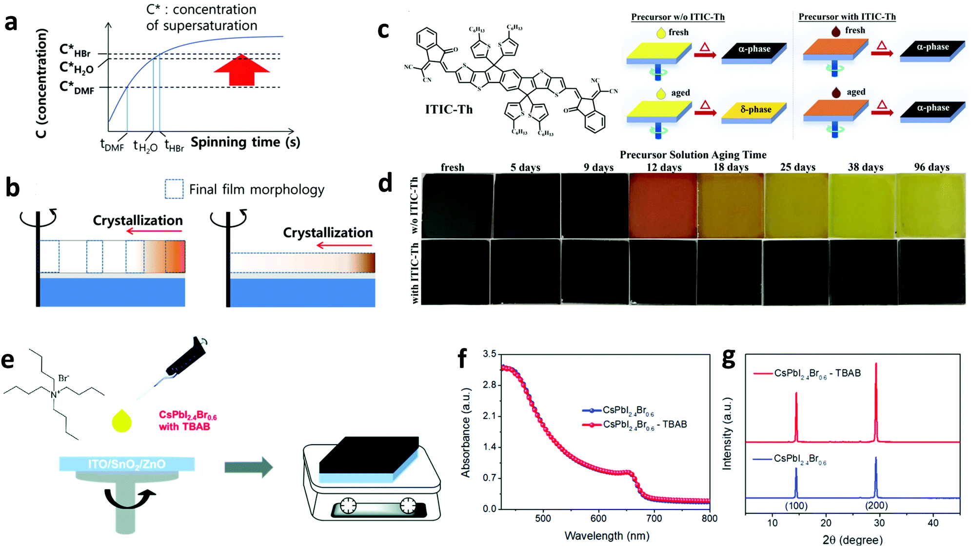 | ||
| Fig. 10 Schematic illustration of the crystallization process during spin-coating. (a) The relation between concentration and spinning time: C* = concentration of supersaturation, t = onset of nucleation time; and (b) the onset of crystallization with MAPbBr3 solution with different solubility by spin-coating (dotted rectangle = the morphology of the fully dried MAPbBr3 film, the total areas of the dotted rectangles in the left and the right figure are similar). This figure was adapted from ref. 153 with permission from John Wiley and Sons, Copyright 2014. (c) The chemical structure of ITIC-Th and schematics of the films fabricated from the fresh and aged precursor solutions without and with ITIC-Th. (d) A series of photographs of films fabricated using perovskite precursor solutions aged for different amounts of time without and with ITIC-Th. This figure was adapted from ref. 155 with permission from John Wiley and Sons, Copyright 2018. (e) Structure of TBAB and preparation of CsPbI2.4Br0.6–TBAB films. (f) Absorption spectra and (g) XRD patterns for CsPbI2.4Br0.6 and CsPbI2.4Br0.6–TBAB films. This figure was adapted from ref. 156 with permission from The Royal Society of Chemistry, Copyright 2019. | ||
Furthermore, Jia et al. introduced a series of organic halide salts having different organic cations and halide anions to control the morphology and crystallinity of the perovskite film.156 When adding tetrabutylammonium bromide (TBAB) into the perovskite (CsPbI2.4Br0.6) precursor solution (Fig. 10e) the UV-vis absorption remained unaffected (Fig. 10f), but they obtained a larger grain size and increased crystallinity compared to the reference sample (Fig. 10g), and excellent charge transport properties. The fabricated PSC exhibited a PCE of 15.21%, while also retaining over 93% of this efficiency upon storage in N2 for 1600 hours.
In a recent paper, Liu et al. were able to highly improve the perovskite film quality through the addition of methylamine (MA) into the precursor perovskite solution.157 Their methodology also enabled the effective passivation of shallow electronic defects present at grain boundaries, hence increasing the carrier lifetime. As a result, the fabricated PSCs reached a high maximum PCE of 20.02% (average 18.44%) and a stabilized one of 19.01% under 1 sun illumination. The molecular cross-linking effect of MA on the perovskite grains through intense hydrogen bond interactions was the initiating event for such remarkable PSC performance.
Fullerene materials, self-assembled monolayers (SAMs) and a combination of both have also been proven to be beneficial additives in terms of improving the perovskite film morphology, among other benefits.158,159 Gu et al. used 3-aminopropanoic acid (APA) to modify the crystallinity and improve the coverage on a PEDOT–PSS substrate of their perovskite.160 As a result, a perovskite layer of superior quality with reduced pinholes and surface roughness was obtained. A decent improvement in the device performance was also achieved. Moreover, aniline, benzylamine and phenethylamine additives, when incorporated into the perovskite solution, were found to offer considerable advantages in perovskite film quality.161 In that case, the degree of hydrophobicity arising from the aromatic group and the packing of the molecular additive (i.e. formation of j-aggregates) was found to be the key for improved PSC performance. Simultaneous enhancement in the efficiency and stability of PSCs was obtained upon the application of small benzylamine.
3.3 Passivation of perovskite defects
Due to their ionic character, perovskites exhibit a vast variety of structural imperfections such as intrinsic point defects, 2D extended defects such as grain boundaries and surface defects and 3D defects such as lead clusters.162Fig. 11 illustrates the most important types of imperfections present on the surface or grain boundaries of the polycrystalline perovskite film. They can be summarized as follows: halide (I− and Br−) or cation (such as MA+ and FA+) vacancies, under-coordinated halide anions and lead cations, lead clusters and lead–halide antisite defects. Fig. 11 also illustrates some intrinsic point defects that form shallow level traps, such as I− or MA+ vacancies, in the bulk of the material. Strong non-radiative recombination losses arise from these defects, which are detrimental to solar cell performance. Therefore, effective defect passivation using molecular additives represents one of the most prominent methods to improve the PSC performance. In the right part of Fig. 11 two commonly applied approaches to passivate such defects, i.e., the introduction of fullerene derivatives that act as Lewis acids and the conversion of the perovskite surface into a wide bandgap material, are also shown.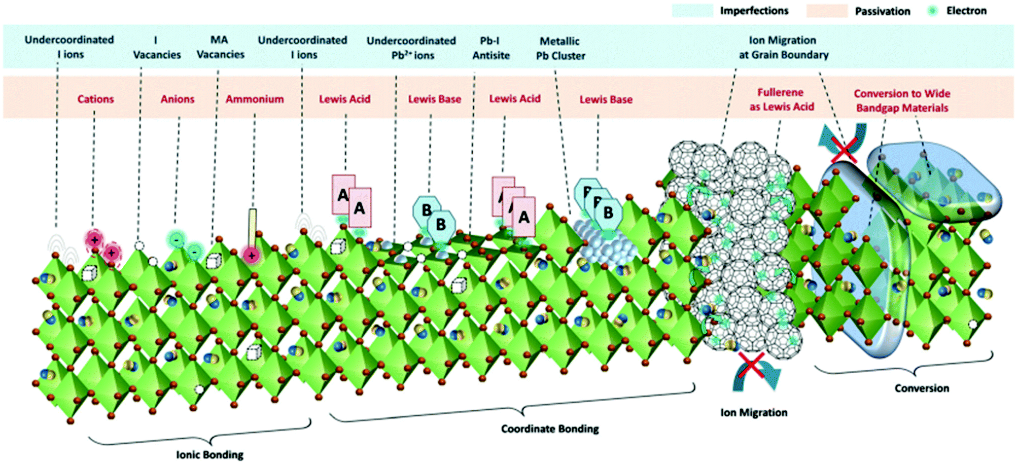 | ||
| Fig. 11 The different defects present at the surface and grain boundaries of the perovskite film. Examples of their passivation by ionic or coordinate bonding and conversion to wide bandgap perovskites are also illustrated. This figure was adapted from ref. 162 with permission from The Royal Society of Chemistry, Copyright 2019. | ||
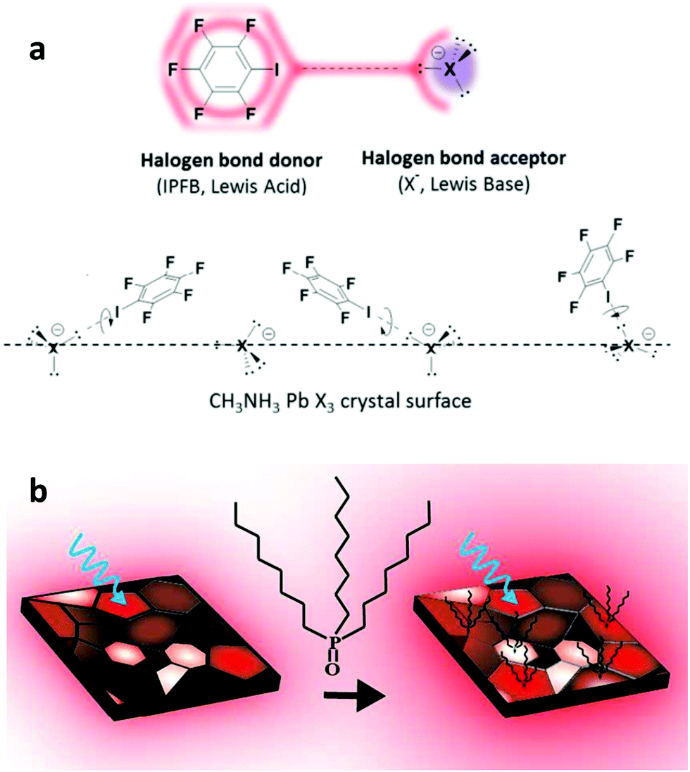
Fullerene derivatives such as PCBM and ICBA have been widely applied as passivation additives in addition to manipulating the morphology of the perovskite absorber.163,164 They represent commonly applied cases of defect passivation additives that act as Lewis acids due to their excellent electron accepting capability. Xu et al. reported the first application of PCBM as a passivation agent added into the perovskite precursor.165 They found that PSCs based on hybrid PCBM–perovskite solids exhibited significantly reduced hysteresis and recombination losses. They explained their results through the assumption that PCBM molecules passivate Pb–I antisite defects during their implementation within the perovskite film. They supported these arguments by theory and experiments. Abate et al. have applied an iodopentafluorobenzene (IPFB) additive to passivate the under-coordinated halide ions.166 They found that the electron deficient nature of this additive makes it behave like an electron acceptor, hence forming strong halogen bonding with the under-coordinated halide or lead–halide antisite defects (Fig. 12a). They showed that trap states at the perovskite were sufficiently passivated through this supramolecular halogen bond complexation between the additive and the perovskite. PSCs with a maximum PCE of 15.7% and a stabilized one of 15% were obtained, demonstrating the effectiveness of their approach.
 | ||
| Fig. 12 (a) Schematic view of the halogen bond interaction between iodopentafluorobenzene, which acts as an electron donor, and a halogen anion in the perovskite, which acts as an electron acceptor. This figure was adapted from ref. 166 with permission from the American Chemical Society, Copyright 2014. (b) Illustration of the perovskite passivation upon the adsorption of a base molecule within the grain boundaries. This figure was adapted from ref. 169 with permission from American Chemical Society, Copyright 2016. | ||
Oxygen-containing alkylphosphine oxides and phosphorus-containing alkylphosphines have been used as effective additives to passivate perovskite defects.167–170 DeQuilettes et al. investigated the effect of Lewis base, namely trioctylphosphine oxide (TOPO), treatment of a polycrystalline perovskite absorber (Fig. 12b).169 They witnessed a huge increase in the photoluminescence quantum yield (PLQY) and carrier lifetime upon base treatment. These results demonstrated the effectiveness of Lewis bases in passivating defect sites, hence prolonging the radiative recombination lifetime.
Alkyl-ammonium additives have also been found to act as passivation agents via the formation of a perovskite material of lower dimensions.171,172 Utilization of phenylethylammonium (PEAI) as a defect modifier was proven to be beneficial for PSCs, which reached a maximum PCE of 23.32%.173 The formation of a layered perovskite on top of the 3D absorber induced favourable electronic coupling at the 3D/2D interface, hence lowering the energetic barrier for charge extraction. The use of cationic atoms and molecules, such as those bearing ammonium groups, has shown great potential for passivation. Moreover, molecules like lead chloride (PbCl2), methyl ammonium chloride (MACl), formamidinium chloride (FACl), and caesium chloride (CsCl) that bear anions (i.e. Cl1−) also enabled effective passivation or doping of the perovskite material.174–176 The chlorine anion has also been shown to alter the thin film morphology and crystallization, hence providing large grains with smooth discontinuities around those grains.
3.4 Modulation of energetics at heterointerfaces
The energetic alignment at the perovskite absorber/charge transport material heterointerfaces influences the charge transport/extraction efficiency and, therefore, the overall device performance.177 Whereas the commonly followed strategy to achieve energy level alignment is the selection of appropriate hole/electron transport materials, adjusting the energy level position of halide perovskites through additives represents an additional, easy to implement methodology. This can be achieved through appropriate p- or n-type doping at the perovskite/HTL or perovskite/ETL heterointerfaces, respectively. The doping mechanism is based on surface/interface charge transfer.In a representative example, Habisreutinger et al. introduced 4-tert-butylpyridine to serve as a p-dopant of the perovskite layer at the heterointerface with the HTL.178 They were able to achieve a significant increase in charge collection efficiency, hence boosting the PSC performance. Wu et al. applied 2,3,5,6-tetrafluoro-7,7,8,8-tetracyanoquinodimethane (F4TCNQ) not only to alter the perovskite energetics but also to induce significant conductivity enhancement through n-type doping and modify the perovskite/ITO energetics via favourable band bending.179 In another study, Noel et al. treated the perovskite film with a strongly oxidizing molybdenum tris(dithiolene) complex (Fig. 13a).180 They achieved a significant WF shift of the perovskite surface indicative of p-doping (Fig. 13b). They also obtained suppression of the carrier lifetime upon Mo-doping, which indicated fast charge transfer at the perovskite/cathode heterointerface (Fig. 13c).
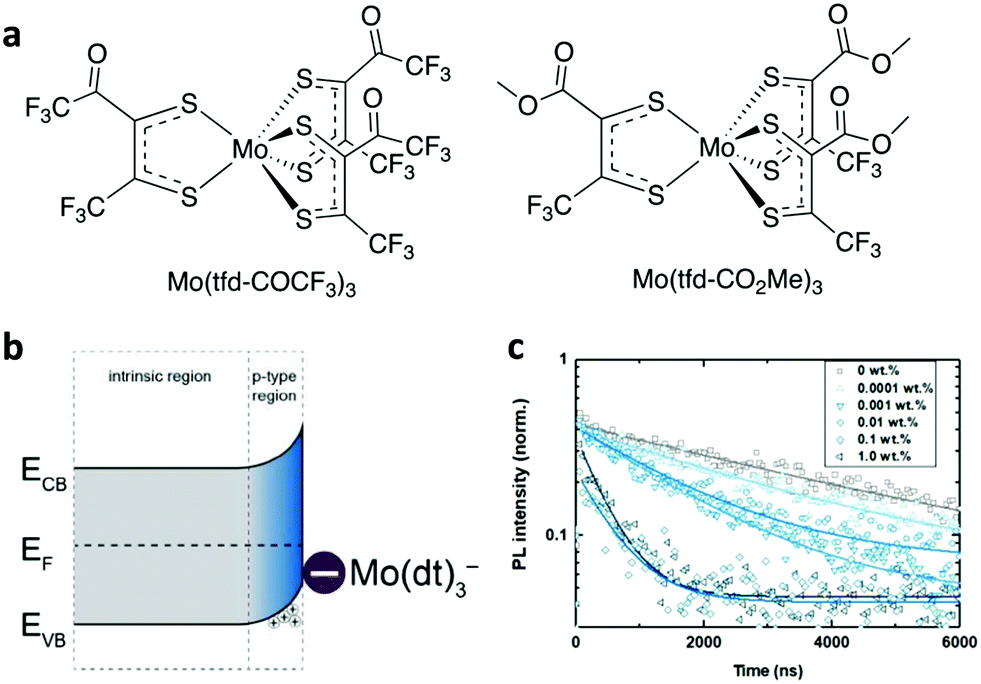 | ||
| Fig. 13 (a) Chemical structures of Mo(tfd-COCF3)3 and Mo(tfd-CO2Me3)3. (b) Illustration of proposed band bending at the surface of the perovskite crystal due to the charge-transfer reaction with Mo(tfd-CO2Me3)3. (c) Time-resolved photoluminescence of neat and Mo(tfd-COCF3)3-treated perovskite films. This figure was adapted from ref. 180 with permission from The Royal Society of Chemistry, Copyright 2019. | ||
The resultant p-doped interface presented improved hole-selectivity, leading to a remarkable PCE of 21%. Wang et al. applied choline iodine (CHI) molecules to simultaneously passivate the trap state density and tune the energetic level alignment at the heterointerfaces.181 CHI was found to improve the perovskite film nanomorphology, enhance the carrier lifetime and tune (decrease) WF, hence improving the contact selectivity. These effects synergistically contributed to highly reproducible and stable PSCs with efficiencies reaching 18.4% under 45 ± 5 °C ambient conditions. Blending F4TCNQ into the perovskite absorber also caused efficient charge transfer, resulting in efficient p-doping at the perovskite and ITO electrode.182 Similar p-doping with F4TCNQ has been employed to electronically couple an inorganic perovskite absorber (CsPbI3) with the anode using either cobaltocenes or zethrenes as dopants.183,184 In these cases, n-type doping was realized by coating this molecule onto the perovskite absorber. WF was properly adjusted at the heterointerface to enable efficient electron transfer.
3.5 Enhancement of the perovskite crystal quality
Enhancing preferential orientation of perovskite nanocrystals represents an effective way to increase thin film crystallization, hence improving the optoelectronic properties. Recently, Zheng et al. reported an increase in grain orientation by using a trace amount of surface-anchoring alkylamine ligands (AALs) having different chain lengths as grain and interface modifiers.185 They demonstrated that the long-chain AALs added to the precursor solution allowed for a prominent (100) orientation and lowered the trap-state density, hence highly suppressing non-radiative recombination and improving the optoelectronic properties of mixed-cation mixed-halide perovskite films. They also showed that whereas the VBM and CBM of the AAL-modified films were nearly identical to those of the pristine one, WF was significantly decreased, indicating effective n-doping upon the addition of AALs into the perovskite. This was attributed to a change of the surface termination of the perovskite absorber upon AAL modification. These n-doped perovskite films enabled more efficient charge transfer to the adjacent ETL (C60). As a result, the fabricated p–i–n planar PSCs exhibited a record PCE of 23%.In a different study, Shao et al. demonstrated improvement in the crystallinity of 3D formamidinium tin iodide (FASnI3) grains, strengthening their orientation in the out-of-plane direction and increasing their size by incorporating ethylammonium iodide (EAI) into a 2D/3D tin perovskite film (where the 2D component is PEA2FASn2I7, PEA = phenylethylammonium) (Fig. 14a and b).186 As a result they were able to decrease charge recombination losses in EAx2D/3D based devices, which exhibited a higher PCE (8.4%) and better reproducibility compared to the reference devices without the additive. Liang et al. reported an effective method to control the rate of perovskite crystallization by incorporating rationally chosen additives into the perovskite precursor solutions.187 The processing additives (i.e., 1,8-diiodooctane, DIO) simultaneously facilitated nucleation (Fig. 14c) and modulated the kinetics of crystal growth during crystallization, leading to a much smoother perovskite morphology with improved coverage area and crystal uniformity. As a result, they enabled high PCE (∼12%) planar-heterojunction solar cells to be fabricated through low-temperature solution processes (under 150 °C).
 | ||
| Fig. 14 Schematic illustration of the (a) EAx3D and (b) EAx2D/3D samples. This figure was adapted from ref. 186 with permission from Elsevier, Copyright 2019. (c) Schematic diagram of the transient chelation of Pb2+ with DIO. This figure was adapted from ref. 187 with permission from John Wiley and Sons, Copyright 2014. | ||
3.6 Multifunctional molecular modulators
In order to obtain enhanced phototovoltaic performance and improved stability of PSCs, it is imperative to simultaneously improve more than one of the detrimental factors such as poor thin film morphology, density of defect states, crystal quality etc.188,189Towards this goal, molecular design of multifunctional molecular materials that modulate the perovskite performance through improvements in several factors has recently been demonstrated.
In a relevant study, Gratzel and co-workers employed a molecular design strategy to improve the electronic properties and photovoltaic performance, as well as strengthen the interaction of FA0.9Cs0.1PbI3 adopted as the perovskite absorber with the electron and hole transport interlayers to ascertain rapid charge carrier extraction.190
To achieve such a goal, they designed a multifunctional molecular modulator (MM) with thiol-based 5-(methylthio)-1H-tetrazole (S), ammonium-based anilinium iodide (N), and bifunctional 3-(5-mercapto-1H-tetrazol-1-yl)benzenaminium iodide (SN) embedded in its structure. This MM featured hydrophobic (hetero)aromatic cores that were further functionalized with ammonium and thiol groups in order to interact with specific components of the perovskite phase and ensure effective defect passivation. They found that the molecular modulator containing only ammonium groups (–NH3+) (termed modulator N) effectively passivated the A cation vacancy defects. The modulators containing thiol-functional groups (–SH) (termed modulator S) could effectively passivate unsaturated Pl2+ ions, while also increasing the grain size of the absorber. The multifunctional molecular modulator termed SN, which combined the advantages of S and N, resulted in significant enhancement in crystallinity and reduced the density of defects that caused non-radiative charge carrier recombination. Furthermore, by using this strategy, these authors were able to remarkably improve the perovskite film morphology through the formation of large grains of superior quality, hence achieving a PCE of over 20% for cells based on the (FAI)0.9Cs0.1(PbI2)1.05 composition. Large active area devices (areas above 1 cm2) also showed excellent operational stability. This excellent PSC performance paved the way for the development of a novel generation of multifunctional molecular modulators (MMs) that enable simultaneous improvements within the photovoltaic device, hence advancing PSC research and practical applications. Therefore, taking into account the recent approaches in molecular additives for perovskite solar cells, additional effort could be spent on the development of multifunctional materials that synergistically contribute to the improvement of two or more perovskite absorber and/or device components in order to simplify the fabrication process and remarkably boost the performance of the fabricated cells. The molecular materials used as additives in PSCs discussed here are summarized in Table 3.
4. Molecular materials as electron transport layers in perovskite solar cells
The ETL serves as an important medium as it transports the photogenerated electrons from the perovskite layer towards the respective contact.191,192 For a molecular material to act as an efficient ETL, a prerequisite is for it to possess a minimized energy difference between its lowest unoccupied molecular orbital (LUMO) and the conduction band minimum (CBM) of the perovskite absorber. Furthermore, the ETL should possess appropriate physical properties and robustness and completely cover the perovskite layer to prevent moisture and air ingress, which degrades the stability of PSCs.193Titanium dioxide (TiO2) has been the most common ETL for the mesoporous and planar n–i–p PSC configurations. But its high thermal post-treatment and intense photocatalytic activity represent severe limitations for the device performance and mass production. Moreover, with the exploration of a variety of novel perovskite semiconductor materials there is an increasing need to design novel, high performing ETLs that will accomplish perfect matching (i.e. energetic) with the novel absorbers, maximizing the device performance. Molecular materials represent a unique platform for designing and developing novel electron transport materials (ETMs) using facile and easy to implement synthetic approaches. In this subsection we highlight the basic design guidelines and synthetic routes as well as strategies and approaches for implementing and modifying the ETL/perovskite interface with a variety of molecular materials. Examples include fullerene derivatives, non-fullerene oligomers, ionic liquids, molecular dyes and inorganic molecular materials.
4.1 Fullerene derivatives
Fullerene derivatives have been for many years the n-type acceptor material of choice for the active layer of organic solar cells. They present attractive optoelectronic properties for use as ETLs such as high electron conductivity and transparency within the visible spectrum. They are now broadly used as ETLs in PSCs, especially in inverted planar structures, where the ETL is deposited on top of the perovskite absorber (Fig. 15a). As an example, Sun et al. demonstrated that a fullerene ETL forms anion–π interactions with the perovskite material (Fig. 15b), enhancing the performance and the stability of PSCs.194 Their experimental findings showed that the fullerene activates relatively inert halide anions such as bromine and chlorine and initiates an n-doping process by forming anion–π interactions, hence facilitating charge transport (Fig. 15c) and suppressing hysteresis. Shao et al. demonstrated PCBM's ability to restrain the severe hysteresis of PSCs via trap state passivation.195 The same authors later showed that solvent annealing makes PCBM more ordered, which increased Voc from 1.04 to 1.13 V without sacrificing Jsc and the FF.196 Consequently, an increase in the PCE from 17.1 to 19.4% was obtained with a simultaneous improvement in the device stability. Similarly, Luo et al. fabricated an inverted PSC structure with PCBM as the ETL and reached an improved PCE of 20.9%.197 Chiang et al. used PCBM to fabricate a PSC consisting of a perovskite–PCBM layer that showed a smooth morphology, increasing Voc and the FF with no hysteresis.198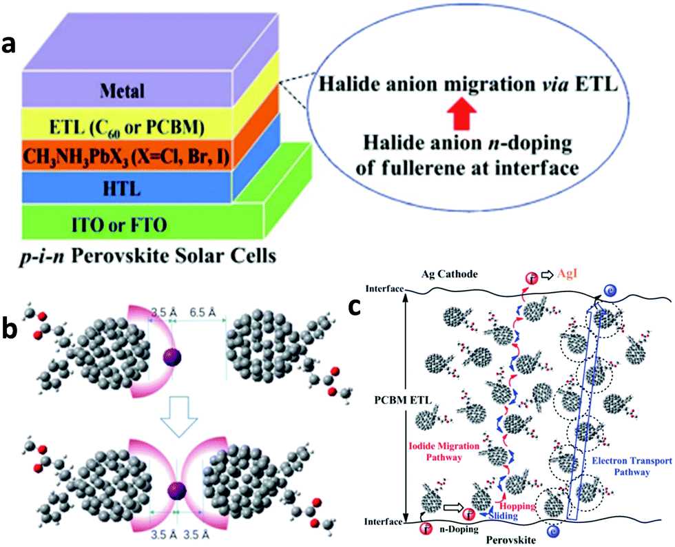 | ||
| Fig. 15 (a) The device structure and the migration of the halide anion through the fullerene layer involving halide anion–π non-covalent interactions. (b) The iodide ion moves from one PCBM molecule to the neighbouring one. (c) Schematic of the migration of iodide within the PCBM layer. This figure was adapted from ref. 194 with permission from The Royal Society of Chemistry, Copyright 2017. | ||
In regular PSCs, one of the most commonly used ETLs is titanium dioxide (TiO2). A viable strategy to overcome the highly defective nature of TiO2 is to insert a thin overlayer of PCBM between the ETL and the perovskite.199 Moreover, hydroxylated fullerene, fullerenol and C60NH2 fullerene derivatives have been successfully employed as interlayers between TiO2 and perovskite layers to reduce the device hysteresis while also improving the performance and stability.200,201 Pyridine-functionalized fullerene derivatives have also been synthesized and used in PSCs as ETLs instead of TiO2.202,203 Liu et al. reported the synthesis of a novel pyridine-functionalized PC60BM (PyCEE) (Fig. 17a) to replace the TiO2 ETL in PSCs (Fig. 16b).202 Due to the suitable energy levels and high electron mobility of PyCEE, the fabricated PSCs achieved a maximum PCE of 18.27% with significantly suppressed hysteresis (Fig. 16c). Moreover, the novel ETL was applied in flexible PSCs, which attained a PCE of 15.25% (Fig. 16d).
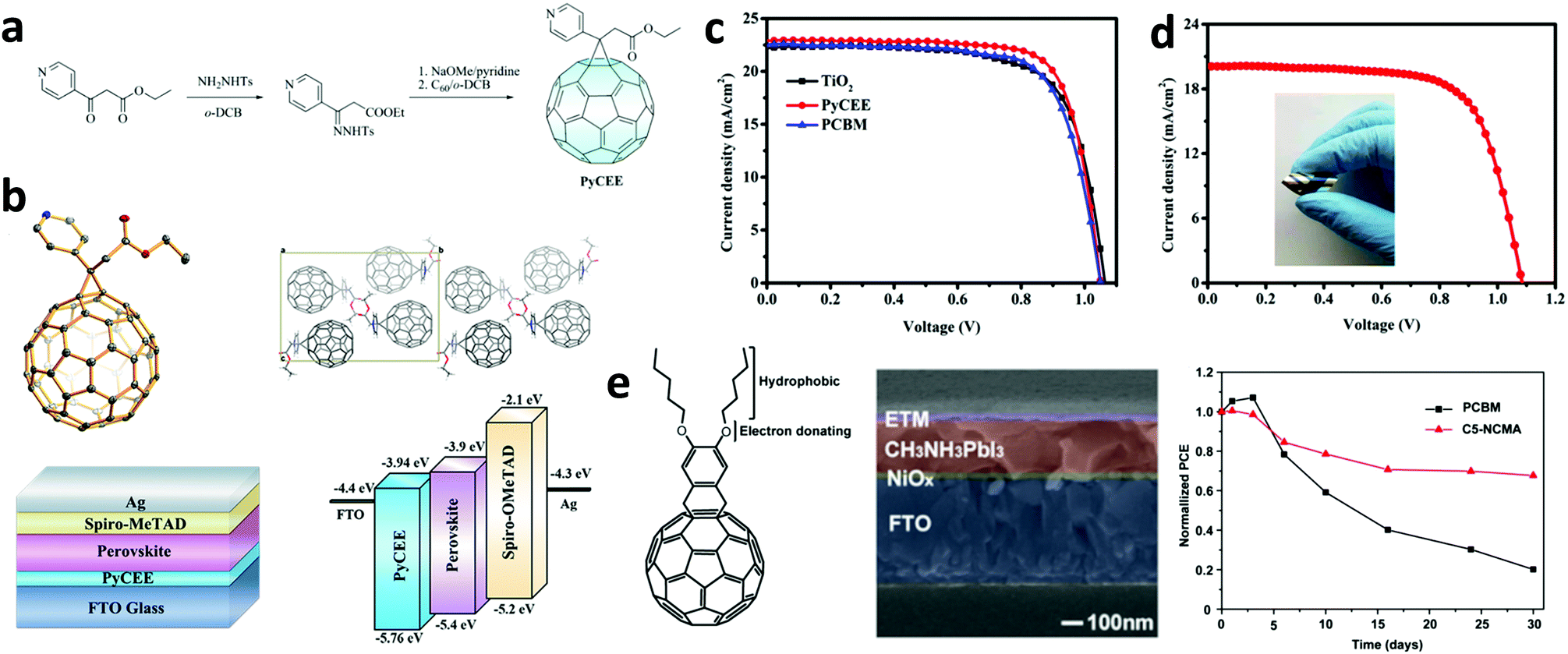 | ||
| Fig. 16 (a) The synthetic procedure of PyCEE. (b) The chemical structure (up, left) and crystal stacking of PyCEE viewed along the a-axis (up, right). The perovskite device architecture (down, left) and the corresponding energy level diagram (bottom, right). (c) J–V characteristic curves of the best-performing PSCs fabricated on glass substrates. (d) J–V characteristic curves of flexible PSCs with PyCEE as the ETL. The image of the flexible device is shown as an inset. This figure was adapted from ref. 202 with permission from American Chemical Society, Copyright 2019. (e) Molecular structure of C5-NCMA (left), cross-section SEM image of the PSC structure with C5-NCMA (middle) and results from the stability test of the PSCs using PCBM (the initial PCE was 15.24%) and C5-NCMA (the initial PCE was 17.04%) (right) as ETLs. This figure was adapted from ref. 209 with permission from Elsevier, Copyright 2016. | ||
Doping of fullerenes to advance their functionality as ETLs in PSCs has also been employed. Yan et al. used conductive fullerene surfactants such as FPPI, Bis-FPPI, Bis-FIMG, and Bis-FITG,204 which highly improved the electron transfer from the perovskite layer towards the electron selective contact. Kakavelakis et al. introduced the doping of PCBM with reduced graphene oxide (rGO).205 With 5% doping, they demonstrated an enhancement in the electron transport capability of PCBM and improved the device efficiency from 12.9% to 14.5%. When cetyl trimethyl ammonium bromide (CTAB) surfactant was applied as a dopant for the PCBM ETL, an enhancement of the electron transport properties of the latter was observed, attributed to a five-fold improvement in electrical conductivity.206 The fabricated PSCs delivered a high PCE in both small and large area devices. Xing et al. combined fullerenes with electron-rich functional groups such as oligoether (OE) side groups,207 and succeeded in simultaneously passivating the interface trap states of the perovskite and reducing WF of the PCBM ETL. Bai et al. attached hydrophobic functional groups to PCBM which was also doped with methylammonium iodide to increase its conductivity by more than 100-fold.208 As a result, the fabricated PSCs showed an improved PCE and were also able to retain nearly 90% of their initial efficiency after 30 days of ambient air exposure. Meng et al. developed a new fullerene derivative named C5-NCMA to replace PCBM in planar p–i–n PSCs (Fig. 17e).209 C5-NCMA featured higher hydrophobicity and a higher LUMO level compared to PCBM. The fabricated devices reached a maximum PCE of 17.6% (which was higher than that of PCBM, i.e., 16.1%) with negligible hysteresis. Generally, fullerene derivatives have been proven to be highly beneficial as ETLs and interlayers in both the regular and the inverted PSC architecture. Their high electron mobilities and appropriate LUMO levels contribute to enhanced device efficiency. However, their prone to oxidation nature raises concerns regarding their compatibility with stable and resilience to oxygen induced degradation solar cells.
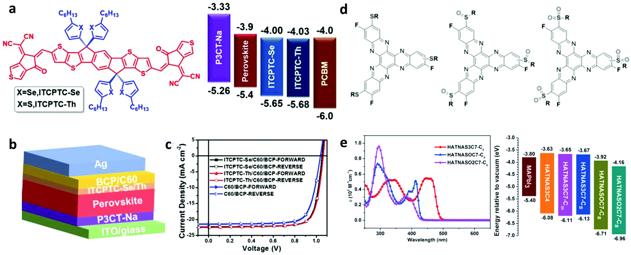 | ||
| Fig. 17 (a) Molecular structures of ITCPTC-Th/Se, and the energy level diagram of each layer in inverted PSCs. (b) PSC architecture and (c) forward and reverse J–V characteristic curves of PSCs with and without the ITCPTC-Se/Th interlayer. This figure was adapted from ref. 213 with permission from The Royal Society of Chemistry, Copyright 2018. (d) The F-substituted HATNA structures and (e) UV/vis absorption spectra of HATNAS3C7-Cs, HATNASOC7-Cs, and HATNASO2C7-Cs in CHCl3 showing molar extinction coefficients (left) and corresponding energy levels of the HATNA derivatives (right). This figure was adapted from ref. 216 with permission from John Wiley and Sons, Copyright 2016. | ||
4.2 Non-fullerene oligomers
Despite the great success of fullerene derivatives as ETLs in PSCs, their further application is limited by poor ambient and thermal stability, cumbersome energy level tunability and high production cost. Therefore, in recent years, much effort has been devoted to the development of alternative materials to be used as ETLs in order to overcome these obstacles. Perylene diimides represent well-established n-type oligomers that possess LUMO levels well-matched with the CBM of most perovskite materials. A series of perylene diimide (PDI) based polymers (Px-PDIs) with different conjugated units, vinylene (V), thiopnene (T), selenophene (Se), dibenzosilole (DBS) and cyclopentadithophene (CPDT), were thus developed for application as alternative ETLs in p–i–n PSCs.210 They exhibited some attractive characteristics such as tunable energy levels, controllable aggregate formation, and smooth film formation. The PSC with PV-PDI achieved a PCE of 10.9%. Im's group used a non-fullerene compound, namely N,N′ bis(phenylmethyl)naphthalene-1,4,5,8-tetracarboxylic diimide (NDI-PM),211 as an alternative ETL in planar PSCs based on various perovskite absorbers. These devices exhibited high thermal stability due to the formation of strong hydrogen bond interactions.In another study, a perylene derivative termed TPE-PDI4 was applied as the ETL in inverted PSCs.212 The modified devices achieved a high PCE of 18.78% when a TPE-PDI4/C60 heterojunction was used as the ETL. Moreover, the high water resistance of the perylene derivative improved the device ambient stability to over 200 h.
Wu et al. applied two π-conjugated molecules, rigid ladder-type derivatives of ITCPTC with two side chains thiophene (ITCPTC-Th) and selenophene (ITCPTC-Se) (Fig. 17a),213 as ETLs in perovskite solar cells (Fig. 17b). Specifically, the ITCPTC-Th device exhibited a PCE of 17.11% (Fig. 17c). The smaller surface roughness and more ordered molecular packing suggest better contact between the ETL and the underlying perovskite layer, facilitating electron transfer. To reduce the hysteresis index (HI), Jian Zhang's group introduced three non-fullerene acceptors, ITIC, ITIC-Th, and IT-M, as ETLs in inverted PSCs.214 The HI of the ITIC, ITIC-Th, and IT-M based devices was 1.78, 1.35, and 1.83, respectively, compared to that of the PCBM based device, which was 3.37. These lower HIs were attributed to the smooth film morphology, the reduction of recombination losses and the passivation of the photoactive layer. Furthermore, Karuppuswamy et al. combined benzo[ghi]perylenetriimide (BPTI) and one more derivative (t-BPTI) as ETLs in inverted PSCs.215 Improved performance, as well as reduced hysteresis, was achieved for the non-fullerene devices. Hexaazatrinaphthylene (HATNA) derivatives have also been successfully shown to function as efficient electron-transporting materials in PSCs, having comparable characteristics with fullerene materials.216 However, issues such as poor solubility are yet to be overcome. The same group replaced three F groups of HATNA-F6 with three alkylsulfanyl chains of different lengths (Fig. 17d and e) and demonstrated a PCE of 17.6% in the PSCs. Summarizing the above, non-fullerene oligomers represent a wide class of highly promising materials with desired optoelectronic properties and adequate resistance to oxidation for application in efficient as well as stable PSCs.
4.3 Ionic liquids
In addition to the molecular materials mentioned above, a few other classes have also been successfully applied as ETLs in PSCs.217 Among them, ionic liquids (ILs) have gained much interest due to their exceptional electrochemical and thermal stability, high electron mobility, large ionic conductivity, intrinsic hydrophilic nature and superior transmittance. Yang et al. employed 1-benzyl-3-methylimidazolium chloride solid-state (ss-IL) ionic liquid [BMIM]Cl via solution processing as an effective ETL in flexible PSCs (Fig. 18a).218 The device with the ss-IL exhibited a high PCE of 16.09%, attributed to the facile electron transfer from the perovskite absorber towards the selective contact, while also showing suppressed hysteresis in the J–V measurements. The authors attributed the improved device performance to the superior characteristics of their ss-IL such as antireflection, high electron mobility, and low WF and a reduced interface trap density of the perovskite material. In addition, ss-IL coated substrates influenced the nanomorphology of the perovskite absorber coated on top of them (Fig. 18b), since the hydrophilicity of the ss-IL was beneficial to the perovskite film formation, resulting in a smoother film surface. Moreover, Yang et al. reported a drastic improvement in PSC performance upon surface optimization of the TiO2 ETL (Fig. 18c and d), using an IL, in particular, 1-butyl-3-methylimidazolium tetrafluoroborate [BMIM]BF4, that showed superior electron mobility and high optical transparency.219 The device PCE was promoted to as high as 19.62% (the certified efficiency was 19.42%), showing also almost no hysteresis (Fig. 18e). This remarkable enhancement of the device performance was mainly attributed to the improved electron mobility and reduced WF of IL-modified TiO2, leading to well-matched energy levels with those of the perovskite absorber. Moreover, the IL modifier suppressed charge accumulation, resulting in increased device stability. Wu et al. studied two ILs with different ions as both independent ETL and TiO2 surface modifiers in planar PSCs.220 It has been demonstrated that the device with the ionic liquid 1-methylimidazolium iodide [EMIM]I used as an independent ETL showed low performance (a PCE value of 9.17%) attributed to the poor film forming properties of [EMIM]I on top of the FTO substrate. One the other hand, the PSC based on the [EMIM]I-modified TiO2 ETL exhibited a high PCE value of 18.08% when compared with the reference device. In the same work, the application of [EMIM]PF6 was also investigated as an independent ETL and TiO2 surface modifier. The PSC with the IL-modified TiO2 exhibited a PCE value of 19.59%, while the device based on the independent [EMIM]PF6 ETL showed a PCE of 14.39%. The introduced IL was beneficial to the crystallinity and film coverage of the perovskite absorber, leading to improved electron transport between the active layer and the selective electrode, as well as reduced recombination losses at the perovskite/ETL interface.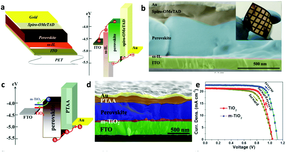 | ||
| Fig. 18 (a) The structure of the flexible PSC with the ss-IL as the ETL (left) and the corresponding energy-level diagram (right). (b) The cross-sectional SEM of a complete device based on the ss-IL ETM. The upper-right inset shows the photograph of the flexible PSCs. This figure was adapted from ref. 218 with permission from John Wiley and Sons, Copyright 2016. (c) Illustration of the energy level diagram of the PSC with [BMIM]BF4 as the TiO2 surface modifier. (d) Representative cross-sectional SEM image of the PSC device. (e) J–V characteristics taken under reverse and forward scan directions. This figure was adapted from ref. 219 with permission from The Royal Society of Chemistry, Copyright 2016. | ||
ILs have also been applied as surface modifiers of zinc oxide (ZnO) ETLs in regular PSCs, leading to effective interface passivation and enhanced long-term device stability. In particular, Zhang et al. employed [EMIM]PF6 between the ZnO ETL and the perovskite absorber,221 achieving a highly efficient and stable device, which was attributed to the effective passivation effect and enhanced electron transport ability of [EMIM]PF6. Chu et al. also investigated the effect of IL modification of the ZnO/perovskite interface in flexible PSCs.222 The employed [BMIM]BF4 improved the crystallinity of the perovskite absorber coated on it, and thus increased the electron extraction efficiency. Consequently, the PCE value of the IL-modified ZnO based device increased by 1.4 times compared to that of the pristine device.
Recently, Huang et al. also studied the effect of IL surface modification of SnO2 used as the ETL in PSCs.223 Upon inserting tetramethylammonium hydroxide (TMAH) into a SnO2 nanoparticle suspension they obtained improved conductivity of the ETL as well as effective passivation at the perovskite surface and grain boundaries. As a result, they promoted the efficiency of their PSCs based on the TMAH-modified SnO2 ETL to over 20%. Furthermore, Xu et al. demonstrated the benefits of ss-ILs as a bilayer ETL (ss-IL/C60) in n–i–p PSCs.224 Upon the application of [EMIM]I on the FTO substrate a significant WF reduction was obtained, leading to a more favorable energy level alignment at the ETL/perovskite interface. In addition, the uniform and smooth perovskite film formation, attributed to the hydrophilicity of the IL, resulted in a reduced defect density and improved device stability. The fabricated PSCs using [EMIM]I as the ETL also exhibited a high PCE value of 15.09%. Furthermore, Li et al. studied the influence of ILs on the performance of inverted PSCs employed at the PCBM/electrode interface.225 They reported that the application of [BMIM]BF4 increased the device efficiency up to 19.3% as a result of facile electron transport/extraction and efficient surface passivation of the PCBM film. As a conclusion from the above results, solution processed ionic liquids may be highly promising as interlayers but mostly as surface modifiers of the ETL in PSCs with the regular architecture. Non-fullerene small molecules and ionic liquids used as ETLs in PSCs are summarized in Table 4.
| ETM | PSC absorber | PCE (%) | J sc (mA cm−2) | V oc (V) | FF | Ref. |
|---|---|---|---|---|---|---|
| PVPDI | MAPbI3 | 10.1 | 16.60 | 0.93 | 0.66 | 200 |
| NDI-PM | MAPbI3 | 18.4 | 21.20 | 1.10 | 0.79 | 201 |
| TPE-PDI4 | MAPbI3 | 16.3 | 21.68 | 1.03 | 0.74 | 202 |
| TPE-PDI4/C60 | MAPbI3 | 18.8 | 21.98 | 1.05 | 0.81 | 203 |
| ITCPTC-Th | MAPbI3 | 17.1 | 21.77 | 1.03 | 0.76 | 203 |
| ITCPTC-Se | MAPbI3 | 16.1 | 21.24 | 1.03 | 0.74 | 203 |
| ITIC | MAPbI3 | 14.0 | 21.25 | 1.08 | 0.61 | 204 |
| ITIC-Th | MAPbI3 | 13.0 | 20.30 | 1.06 | 0.60 | 204 |
| IT-M | MAPbI3 | 11.9 | 20.03 | 1.06 | 0.56 | 204 |
| HATNA-F6 | MAPbI3 | 4.7 | 10.17 | 0.85 | 0.58 | 206 |
| [BMIM]BF4 | MAPbI3 | 19.6 | 22.80 | 1.12 | 0.77 | 210 |
| [EMIM]I | MAPbI3 | 17.2 | 23.70 | 1.10 | 0.66 | 210 |
| [EMIM]PF6 | MAPbI3 | 18.5 | 22.90 | 1.10 | 0.74 | 210 |
| TMAH | MAPbI3 | 20.3 | 22.51 | 1.14 | 0.79 | 213 |
| PCBM/[BMIM]BF4 | MAPbI3 | 19.3 | 23.52 | 1.06 | 0.77 | 215 |
4.4 Molecular dyes
Recently, molecular dyes were also used to modify the quality of the perovskite absorber, mainly through surface energy adjustment of the TiO2 ETL. This is the so-called dye-sensitization approach.226 The introduction of the solution processable triphenylamine-based metal-free organic (E)-3-(5-(4-(bis(2′,4′-dibutoxy-[1,1′-biphenyl]-4yl)amino)phenyl)thiophen-2-yl)-2-cyanoacrylic acid (D35) D–π–A dye modifier sensitizing the titania compact layer (Fig. 19a) led to planar PSCs based on MAPbI3 delivering an enhanced PCE which is accompanied by significantly increased stability. The reported results indicate that the performance enhancement is attributed to improved recombination resistance, increased electron transport, better crystallization of the deposited perovskite (large and homogeneous perovskite crystals) and the humidity sealing character of the hydrophobic dye monolayer, thus demonstrating that dye sensitization can be effectively employed for interface engineering in PSCs.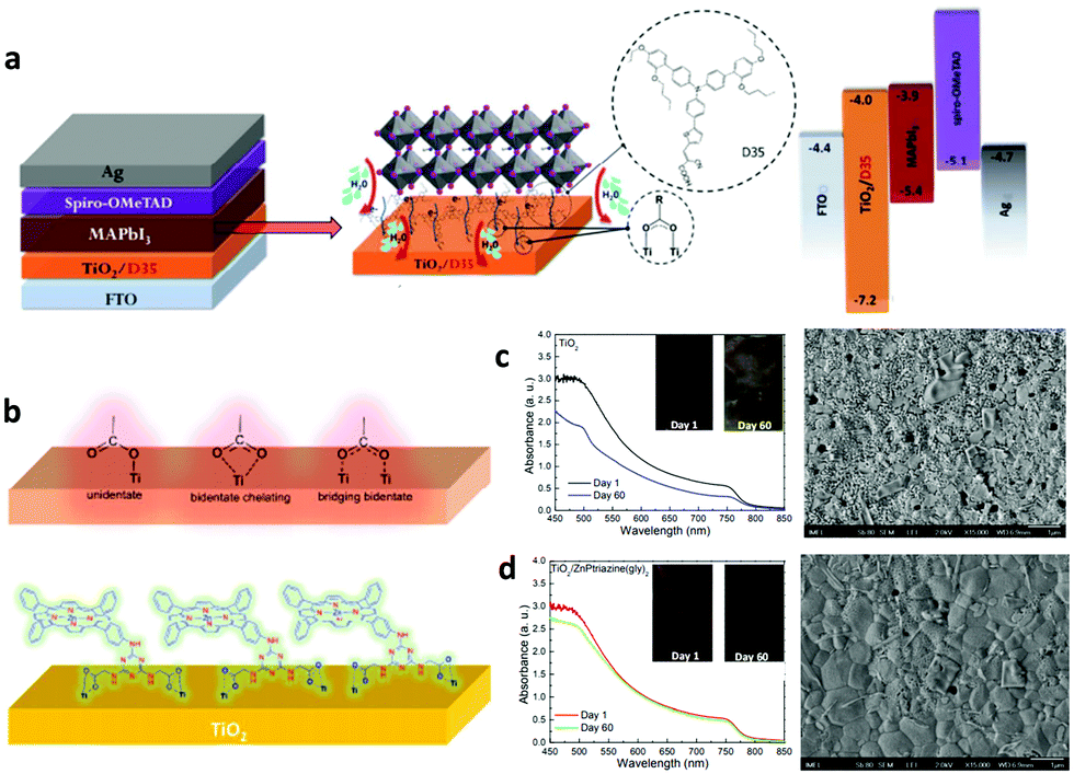 | ||
| Fig. 19 (a) The planar PSC architecture (left) using a D35/TiO2 layer beneath the MAPbI3 absorber (middle) and the corresponding energy band diagram (right). This figure was adapted from ref. 226 with permission from American Chemical Society, Copyright 2018. (b) The anchoring mode of ZnP-BDP on the TiO2 surface. Stability studies of perovskite films on (c) TiO2 and (d) ZnP-BDP modified TiO2 ETLs. This figure was adapted from ref. 229 with permission from the American Chemical Society, Copyright 2018. | ||
The dye-sensitization approach was further justified by effectively simulating the electrical behavior of the PSCs. Three equivalent circuits including single-, double- and triple-diode models were developed for the two types of PSCs (modified by the D35 dye and non-modified) and the electrical parameters were optimally extracted using the elephant herd optimization (EHO) paradigm.227 The simulation results exhibited EHO superiority compared with the competitive algorithms and confirmed a high similarity between the estimated parameters and the experimental ones.
The proposed three diode model was able to better simulate the electrical behavior of PSCs and demonstrated that dye sensitization of the titania compact layer leads to higher performance expressed in terms of low series resistance, high shunt resistance, low diode ideality factor, low diode saturation current, and high open circuit voltage values. Thus, the obtained results further confirmed the advantages of small chromophores (dyes) in shielding charge carrier transport in PSCs due to the interaction between perovskite materials and the dye-coated TiO2 ETL. This work paved the way towards fabricating highly stable PSCs with high PCE as well, through optimizing the titania/perovskite interface and better understanding of its electrical behavior. The EHO formulation offered precious additional information about cell parameters that cannot be estimated using pure experimental electrochemical techniques (e.g., electrochemical impedance spectroscopy – EIS). The performed simulation opens new directions in the field of new efficient mathematical optimization tools that can be used in solving the parameter estimation problem. In addition, a Schiff base cobalt complex derived from ninhydrin and glycine (Co-NG dye) was used as a sensitizer for TiO2 and ZnO in order to improve the electron transfer, and the efficiency and stability of PSCs.228 As a result, the solar cell performances of TiO2/Co-NG and ZnO/Co-NG show a significant efficiency increase compared to the reference solar cells, thus providing significant insights for passivation of the corresponding interfaces of the ETL oxide materials with the perovskite absorber.
Along the same direction, the first application of a porphyrin compound to improve the performance of planar PSCs was also reported.229 In this work, motivated by the excellent electron transfer capability of porphyrin molecules in natural photosynthesis, the insertion of a Zn porphyrin-bodipy (ZnP-BDP) based thin layer between the TiO2 ETL and the perovskite film significantly enhances the efficiency and life time of the corresponding devices (Fig. 19b). The hydrophobic porphyrin was substituted with two glycine moieties bearing carboxylic acid groups for strong anchoring on the metal oxide and one triazine electron withdrawing spacer for accelerating electron transfer. The efficiency enhancement was the result of the large increase in Jsc which originates from the surface passivation of TiO2 and the perovskite film caused by porphyrin molecules and the fast electron extraction, which also reduced recombination losses at the metal oxide/porphyrin/perovskite interface. A decrease in the surface energy of TiO2 also benefitted the nanostructure, improved the crystallinity and slowed the degradation of the perovskite layer (Fig. 19c and d). Conclusively, molecular dyes have been exclusively incorporated in the form of ultra-thin interlayers to act as surface modifiers and/or sensitizers of the commonly used TiO2 ETL in regular PSCs. On the contrary, they have been applied as HTMs in the form of thick and compact films. Their dual functionality derives from the appropriate energetics of both the HOMO and LUMO levels, which generally match the VBM and CBM of the perovskite absorber, respectively, and their ambipolar charge conduction. Taking into account their facile synthesis and ease of modification, such molecules represent a highly promising class of interelectrode materials in PSCs.
4.5 Molecular materials as surface modifiers of ETLs
The aforementioned molecules are also used to modify the properties of ETLs such as the defect density, work function and surface energy besides serving as the ETM themselves. PCBM and fullerene derivatives such as hydroxylated fullerene, fullerenol and C60NH2 fullerene have been applied as surface modifiers of TiO2 in regular architecture PSCs to suppress surface defects and modify WF of the ETL.199–201 Li et al. synthesized a triblock fullerene derivative (termed PCBB-2CN-2C8) via rational molecular design for modifying the TiO2 surface and improving the charge extraction from the perovskite layer.230 Together with its uplifted surface WF, Voc and the FF were dramatically increased from 0.99 to 1.06 V, and from 72.2% to 79.1%, respectively, resulting in a 20.7% improvement in the PCE for the best performing devices. Their findings strongly suggested that PCBB-2CN-2C8 passivated the surface of the TiO2 ETL, hence reducing charge recombination losses. The passivation effect was also supported by stability tests of the PSCs with the shelf lifetime under ambient conditions improved by a factor of more than 4, from ∼40 h to ∼200 h, using PCBB-2CN-2C8 as a surface modifier of TiO2. Ionic liquids have also served as surface modifiers of several types of ETLs such as TiO2, ZnO and SnO2 under the requirement of altering the oxide surface properties (i.e., surface energy) and hence the nanomorphology of the perovskite overlayer.221–223 They also induce a high decrease in the oxide WF through the formation of large negative interfacial dipoles.Liu et al. introduced an organic silane self-assembled monolayer between the TiO2 ETL and the perovskite absorber, resulting in optimized interface band alignments and an enhanced charge lifetime.231 The average PCE was improved from 9.6% to 11.7%, with a highest efficiency of 12.7%, for this low-cost HTL-free PSC.
Furthermore, Jiang et al. successfully applied a novel non-fullerene electron acceptor derivative based on a bulky seven-ring fused core (indacenodithieno[3,2-b]thiophene, IT), end-capped with 2-(3-oxo-2,3-dihydroinden-1-ylidene)malononitrile (INCN) groups, and having four 4-hexylphenyl groups substituted on it.232 Each INCN has one carbonyl and two cyano groups, and these electron-withdrawing groups could downshift the LUMO levels. As a result, this derivative, namely ITIC, possessed low LUMO and HOMO levels and good electron transport ability. Their investigation revealed that ITIC smoothens the TiO2 surface, while also passivating surface defects or dangling bonds and optimizing the device band alignment. In addition, it was demonstrated that the thin ITIC surface modifier promoted the formation of a high quality, uniform perovskite overlayer with better surface coverage and large grain size (Fig. 20). As a result, the device efficiency has been dramatically increased from 17.12% to 20.08%.
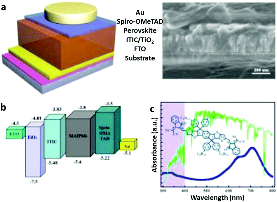 | ||
| Fig. 20 (a) The structure of the perovskite solar cells with ITIC modified TiO2 as the ETL and the cross-sectional SEM of a complete device. (b) Energy level diagram of the perovskite solar cells, exhibiting the collecting process of photogenerated charge carriers. (c) The absorption spectrum and the molecular structure of ITIC. The inset green line is the solar spectrum. This figure was adapted from ref. 232 with permission from The Royal Society of Chemistry, Copyright 2017. | ||
Porphyrin compounds have also been applied as surface modifiers of TiO2 and electron transfer mediators from the perovskite absorber towards the ETL.229 In general, the small size and ease of processing of molecular materials make them ideal for the surface modification of the inorganic ETL commonly used in regular types of PSCs.
4.6 Inorganic molecular materials
Inorganic molecular materials exhibit a significant improvement in chemical and environmental stability and, therefore, they have been extensively investigated in recent years. Transition metal sulfides including cadmium sulfide (CdS), indium sulfide (In2S3), titanium sulfide (TiS2), tin sulfide (SnS) and zinc sulfide (ZnS) have been incorporated as novel ETLs in PSCs. For example, CdS has been employed as an electron extraction/transport layer in both p–i–n MAPbI3 based and n–i–p (CsMAFA)PbI3−xBrx based PSCs with a PCE of 13.36%,233 and 14.28%,234 respectively.In2S3 has also been explored as an ETL to entirely replace TiO2 in n–i–p type MAPbI3 PSCs with PCEs ranging from 15.48%235 to 18.83%.236 More recently, TiS2 replaced TiO2 in n–i–p type PSCs, leading to an enhanced PCE of 17.37% for MAPbI3,237 and 18.79% for (MAFA)PbI3−xClx.238 SnS was also employed as an ETL, replacing TiO2 in n–i–p type MAPbI3 PSCs with a PCE of 13.20%,239 and in p–i–n type (FAPbI3)0.9(MAPbBr3)0.1 based PSCs with a PCE of 18.40%.240 Furthermore, a very high PCE of 20.70% was recently demonstrated in triple cation CsFAMAPbI3−xBrx PSCs with ZnS as an interfacial modifier to facilitate electron transfer at the perovskite/ZnO interface, passivate ZnO defects, reduce undesired interfacial charge recombination and increase UV stability.241Fig. 21a and b illustrate the energy-level diagram and the PCE evolution vs. time (inset: current density vs. voltage) of ITO/ZnO/ZnS/TiO2/CsFAMAPbI3−xBrx/spiro-OMeTAD/Au PSCs with a ZnS ETL.
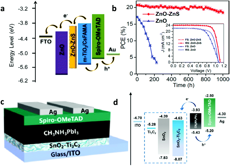 | ||
| Fig. 21 (a) Schematic energy-level diagram and (b) PCE evolution versus time (inset: current density versus voltage characteristics) of ITO/ZnO/ZnS/TiO2/CsFAMAPbI3−xBrx/spiro-OMeTAD/Au perovskite solar cells with ZnS as the ETL. This figure was adapted from ref. 241 with permission from American Chemical Society, Copyright 2019. (c) Architecture and (d) schematic energy-level diagram of ITO/ETL/MAPbI3/spiro-OMeTAD/Ag perovskite solar cells with SnO2–Ti3C2 as the ETL. This figure was adapted from ref. 245 with permission from The Royal Society of Chemistry, Copyright 2019. | ||
2D transition metal carbide nanosheets (MXenes, structure Ti3C2Tx where T is the termination group) with appealing optoelectronic properties such as tunable WF and high charge carrier mobilities have been recently used as effective interfacial modification layers in PSCs. As a result, significantly enhanced device performance was obtained together with improved stability and reduced hysteresis. As an example, Agresti et al. exploited MXenes with different termination groups (F, O and OH) to demonstrate WF tunability and incorporated them as ETLs in n–i–p type (CsFAMA)PbI3−xBrx based PSCs with PCEs reaching 20.14%.242
Interface dipoles induced at the perovskite/Ti3C2Tx interface tuned the energy level alignment and facilitated charge transport, resulting in substantial improvement of the PSC performance. Further improvement has been made by UV-ozone treated metallic Ti3C2Tx as a novel functional ETL and Ti3C2 as an effective SnO2 metal oxide modifier in n–i–p type MAPbI3 PSCs with PCEs of 17.17%,243 and 18.34%,244 respectively. Moreover, Yang et al. demonstrated PSCs of high efficiency and stability using another member of the MXene family, in particular, Ti3C2. In Fig. 21c and d, the architecture and the schematic energy-level diagram of n–i–p type ITO/ETL/MAPbI3/spiro-OMeTAD/Ag perovskite solar cells with SnO2–Ti3C2 as the ETL are depicted.245 These inorganic ETMs are summarized in Table 5. Despite the fact that these materials do not yet allow for the high efficiencies achieved with organic molecular materials, they, however, offer the possibility of high PSC stability and resilience to environmental degradation due to their chemical stability and robustness.
| ETM | PSC absorber | PCE (%) | J sc (mA cm−2) | V oc (V) | FF | Ref. |
|---|---|---|---|---|---|---|
| CdS | MAPbI3 | 13.4 | 19.73 | 1.01 | 0.67 | 233 |
| CdS | CsMAFAPbI3−xBrx | 14.3 | 20.86 | 1.00 | 0.68 | 234 |
| In2S3 | MAPbI3 | 15.5 | 21.00 | 1.06 | 0.69 | 235 |
| In2S3 | MAPbI3 | 18.8 | 22.98 | 1.10 | 0.75 | 236 |
| TiS2 | MAPbI3 | 17.4 | 23.38 | 1.05 | 0.71 | 237 |
| TiS2 | MAFAPbI3−xClx | 18.8 | 24.75 | 1.00 | 0.75 | 238 |
| SnS | MAPbI3 | 13.2 | 21.70 | 1.01 | 0.60 | 239 |
| SnS | (FAPbI3)0.9(MAPbBr3)0.1 | 18.4 | 22.50 | 1.07 | 0.73 | 240 |
| ZnS | CsFAMAPbI3−xBrx | 20.7 | 24.10 | 1.12 | 0.77 | 241 |
| Ti3C2Tx MXenes | CsFAMAPbI3−xBrx | 20.1 | 23.82 | 1.09 | 0.78 | 242 |
| Ti3C2Tx MXenes | MAPbI3 | 17.2 | 22.63 | 1.08 | 0.70 | 244 |
| Ti3C2 MXene | MAPbI3 | 18.3 | 23.14 | 1.04 | 0.75 | 245 |
5. Conclusions and perspectives
The power conversion efficiency of perovskite solar cells has rapidly increased, exceeding 25% in recent years. This can be attributed to a synergistic improvement in the perovskite material processing and judicious selection and engineering of charge transport layers. To advance the functionality of the latter, the interface engineering approach has been explored in less than a decade. This includes molecular materials, which are promising due to their ease of chemical manipulation and facile preparation at low-cost. Furthermore, such extraordinary small compounds, when included as additives in the precursor solution, have been proven to be capable of doing what inorganic chemistry fails to do, that is to manipulate the perovskite absorber itself and further improve its utility in terms of altering the defect chemistry, bandgap values, non-radiative losses, and nanomorphology.In this review, the different kinds of molecular materials used as charge transport layers or additives in PSCs and their impact on the device performance metrics have been thoroughly discussed. Several classes of molecular materials relying on a variety of central scaffolds decorated with appropriate peripheral groups for improving the solution processability were found to exhibit either strong electron-donating properties, hence acting as excellent HTMs, or strong electron-accepting capabilities, thus being efficient ETMs. Many of these materials such as small molecules require suitable doping to increase their poor conductivity, but others like ionic liquids are self-doped, which is an effective method to achieve high efficiencies without the use of dopants. Inorganic compounds, on the other hand, exhibit intrinsic high conductivity and superior robustness, which render them an attractive class of materials with the potential to contribute to future commercialization of PSCs. Organic compounds, however, will definitely continue being highly important for the PSC architecture due to their ease of chemical modification to satisfy device fabrication criteria.
The potential of additives also acting as healing agents, stabilizers and crystal growth modifiers through their simple inclusion in the perovskite precursor solution or upon their insertion within the perovskite surface via post-treatment has been also investigated. Acting as either Lewis acids or bases, they are capable of forming strong coordination bonds with lead, playing multifunctional roles upon their addition within the perovskite material. Additives are highly desirable, but at the same time reveal the overall complexity of the system in question, making it difficult to give a clear explanation for the underlying mechanisms of device performance improvement.
Despite the large progress in both areas under examination, that of interfacial materials and that of additives, further efforts are needed to design and synthesize novel molecular materials with excellent optoelectronic properties and cost-effectiveness for sophisticated perovskite material and device engineering. Based on this review, the guidance for designing and applying new organic and inorganic molecular charge transport materials includes the use of the careful design of novel molecules possessing high charge carrier mobility, suitable energy levels that allow zero loss during charge transfer while also blocking opposite charge leaking through them, hydrophobicity, good solubility, and low cost. The introduction of suitable functional groups onto the surface of organic interfacial materials is beneficial for facilitating charge carrier extraction or injection.
They should be able to strongly coordinate with the perovskite imperfections, decreasing defect states, increasing hydrophobicity, tuning the nanomorphology and beyond. Small size and tunable composition with either strong acidic or basic character are only a few design rules for future development. We anticipate that with interdisciplinary collaboration between chemistry, materials science and device physics, large progress in the development of such molecular materials will be achieved in the near future.
Conflicts of interest
There are no conflicts to declare.Acknowledgements
M. V. and P. A. acknowledge support of this work from the project “Development of Materials and Devices for Industrial, Health, Environmental and Cultural Applications” (MIS 5002567) which is implemented under the “Action for the Strategic Development on the Research and Technological Sector”, funded by the Operational Programme “Competitiveness, Entrepreneurship and Innovation” (NSRF 2014–2020) and co-financed by Greece and the European Union (European Regional Development Fund). P. F. acknowledges financial support from the European Union's Horizon 2020 Marie Curie Innovative Training Network 764787 “MAESTRO” project. MKN thanks CTI 25590.1 PFNM-NM, Solaronix, Aubonne, Switzerland.Notes and references
- S. D. Stranks and H. J. Snaith, Nat. Nanotechnol., 2015, 10, 391–402 CrossRef CAS PubMed.
- G. E. Eperon, T. Leijtens, K. A. Bush, R. Prasanna, T. Green, J. T.-W. Wang, D. P. McMeekin, G. Volonakis, R. L. Milot, R. May, A. Palmstrom, D. J. Slotcavage, R. A. Belisle, J. B. Patel, E. S. Parrott, R. J. Sutton, W. Ma, F. Moghadam, B. Conings, A. Babayigit, H.-G. Boyen, S. Bent, F. Giustino, L. M. Herz, M. B. Johnston, M. D. McGehee and H. J. Snaith, Science, 2016, 354, 861–865 CrossRef CAS PubMed.
- D. P. McMeekin1, G. Sadoughi, W. Rehman, G. E. Eperon, M. Saliba, M. T. Hörantner, A. Haghighirad, N. Sakai, L. Korte, B. Rech, M. B. Johnston, L. M. Herz and H. J. Snaith, Science, 2016, 351, 151–155 CrossRef PubMed.
- K. A. Bush, A. F. Palmstrom, Z. J. Yu, M. Boccard, R. Cheacharoen, J. P. Mailoa, D. P. McMeekin, R. L. Z. Hoye, C. D. Bailie, T. Leijtens, I. M. Peters, M. C. Minichetti, N. Rolston, R. Prasanna, S. Sofia, D. Harwood, W. Ma, F. Moghadam, H. J. Snaith, T. Buonassisi, Z. C. Holman, S. F. Bent and M. D. McGehee, Nat. Energy, 2017, 2, 17009 CrossRef CAS.
- M. Saliba, T. Matsui, K. Domanski, J.-Y. Seo, A. Ummadisingu, S. M. Zakeeruddin, J.-P. Correa-Baena, W. R. Tress, A. Abate, A. Hagfeldt and M. Grätzel, Science, 2016, 354, 206–209 CrossRef CAS PubMed.
- C. Momblona, L. Gil-Escrig, E. Bandiello, E. M. Hutter, M. Sessolo, K. Lederer, J. Blochwitz-Nimoth and H. J. Bolink, Energy Environ. Sci., 2016, 9, 3456–3463 RSC.
- E. T. Hoke, D. J. Slotcavage, E. R. Dohner, A. R. Bowring, H. I. Karunadasa and M. D. McGehee, Chem. Sci., 2015, 6, 613–617 RSC.
- A. J. Barker, A. Sadhanala, F. Deschler, M. Gandini, S. P. Senanayak, P. M. Pearce, E. Mosconi, A. J. Pearson, Y. Wu, A. R. S. Kandada, T. Leijtens, F. De Angelis, S. E. Dutton, A. Petrozza and R. H. Friend, ACS Energy Lett., 2017, 2, 1416–1424 CrossRef CAS.
- R. J. Stoddard, F. T. Eickemeyer, J. K. Katahara and H. W. Hillhouse, J. Phys. Chem. Lett., 2017, 8, 3289–3298 CrossRef CAS.
- M. Saliba, T. Matsui, J.-Y. Seo, K. Domanski, J.-P. Correa-Baena, M. K. Nazeeruddin, S. M. Zakeeruddin, W. Tress, A. Abate, A. Hagfeldtd and M. Grätzel, Energy Environ. Sci., 2016, 9, 1989–1997 RSC.
- O. D. Miller, E. Yablonovitch and S. R. Kurtz, IEEE J. Photovoltaics, 2012, 2, 303–311 Search PubMed.
- J. Kim, S.-H. Lee, J. H. Lee and K.-H. Hong, J. Phys. Chem. Lett., 2014, 5, 1312–1317 CrossRef CAS PubMed.
- M. L. Agiorgousis, Y.-Y. Sun, H. Zeng and S. Zhang, J. Am. Chem. Soc., 2014, 136, 14570–14575 CrossRef CAS PubMed.
- E. Aydin, M. De Bastiani and S. De Wolf, Adv. Mater., 2019, 31, 1900428 CrossRef PubMed.
- Y. Liu, S. Akin, L. Pan, R. Uchida, N. Arora, J. V. Milić, A. Hinderhofer, F. Schreiber, A. R. Uhl, S. M. Zakeeruddin, A. Hagfeldt, M. I. Dar and M. Grätzel, Sci. Adv., 2019, 5, eaaw2543 CrossRef PubMed.
- S. D. Stranks, V. M. Burlakov, T. Leijtens, J. M. Ball, A. Goriely and H. J. Snaith, Phys. Rev. Appl., 2014, 2, 034007 CrossRef.
- J. Zhang, Q. Sun, Q. Chen, Y. Wang, Y. Zhou, B. Song, X. Jia, Y. Zhu, S. Zhang, N. Yuan, J. Ding and Y. Li, Sol. RRL, 2019, 27, 1900421 Search PubMed.
- H. Kim, K. A. Huynh, S. Y. Kim, Q. Van Le and H. W. Jang, Phys. Status Solidi RRL, 2019, 7, 1900435 Search PubMed.
- C.-I. Chen, S. Wu, Y.-A. Lu, C.-C. Lee, K.-C. Ho, Z. Zhu, W.-C. Chen and C.-C. Chueh, Adv. Sci., 2019, 6, 1901714 CrossRef CAS PubMed.
- K. Morita and T. Michinobu, Synth. Met., 2019, 257, 116179 CrossRef CAS.
- A. Kojima, K. Teshima, Y. Shirai and T. Miyasaka, J. Am. Chem. Soc., 2009, 131, 6050–6051 CrossRef CAS PubMed.
- C. Wehrenfennig, G. E. Eperon, M. B. Johnston, H. J. Snaith and L. M. Herz, Adv. Mater., 2014, 26, 1584–1589 CrossRef CAS PubMed.
- Q. Dong, Y. Fang, Y. Shao, P. Mulligan, J. Qiu, L. Cao and J. Huang, Science, 2015, 347, 967–969 CrossRef CAS PubMed.
- D. Luo, R. Su, W. Zhang, Q. Gong and R. Zhu, Nat. Rev. Mater., 2020, 5, 44–60 CrossRef CAS.
- A. K. Jena, A. Kulkarni and T. Miyasaka, Chem. Rev., 2019, 119, 3036–3103 CrossRef CAS PubMed.
- A. E. Fedorovskiy, N. A. Drigo and M. K. Nazeeruddin, Small Methods, 2020, 4(5), 1900426 CrossRef.
- J. L. Miller, Phys. Today, 2014, 67, 13–15 CrossRef CAS.
- M. A. Green, Y. Hishikawa, E. D. Dunlop, D. H. Levi, J. Hohl-Ebinger and A. W. Y. Ho-Baillie, Prog. Photovoltaics, 2018, 26, 427–436 Search PubMed.
- H. Jin, E. Debroye, M. Keshavarz, I. G. Scheblykin, M. B. J. Roeffaers, J. Hofkens and J. A. Steele, Mater. Horiz., 2020, 7, 397–410 RSC.
- X. Zheng, B. Chen, J. Dai, Y. Fang, Y. Bai, Y. Lin, H. Wei, X. C. Zeng and J. Huang, Nat. Energy, 2017, 2, 17102 CrossRef CAS.
- D. Luo, W. Yang, Z. Wang, A. Sadhanala, Q. Hu, R. Su, R. Shivanna, G. F. Trindade, J. F. Watts, Z. Xu, T. Liu, K. Chen, F. Ye, P. Wu, L. Zhao, J. Wu, Y. Tu, Y. Zhang, X. Yang, W. Zhang, R. H. Friend, Q. Gong, H. J. Snaith and R. Zhu, Science, 2018, 360, 1442–1446 CrossRef CAS PubMed.
- P. Liu, X. Liu, L. Lyu, H. Xie, H. Zhang, D. Niu, H. Huang, C. Bi, Z. Xiao, J. Huang and Y. Gao, Appl. Phys. Lett., 2015, 106, 193903 CrossRef.
- A. Miyata, A. Mitioglu, P. Plochocka, O. Portugall, J. T.-W. Wang, S. D. Stranks, H. J. Snaith and R. J. Nicholas, Nat. Phys., 2015, 11, 582–587 Search PubMed.
- W. H. Nguyen, C. D. Bailie, E. L. Unger and M. D. McGehee, J. Am. Chem. Soc., 2014, 136, 10996–11001 CrossRef CAS PubMed.
- G. Niu, X. Guo and L. Wang, J. Mater. Chem. A, 2015, 3, 8970–8980 RSC.
- P.-L. Qin, H.-W. Lei, X.-L. Zheng, Q. Liu, H. Tao, G. Yang, W.-J. Ke, L.-B. Xiong, M.-C. Qin, X.-Z. Zhao and G.-J. Fang, Adv. Mater. Interfaces, 2016, 3, 1500799 CrossRef.
- J. A. Raiford, R. A. Belisle, K. A. Bush, R. Prasanna, A. F. Palmstrom, M. D. McGehee and S. F. Bent, Sustainable Energy Fuels, 2019, 3, 1517–1525 RSC.
- E. L. Ratcliff, B. Zacher and N. R. Armstrong, J. Phys. Chem. Lett., 2011, 2, 1337–1350 CrossRef CAS PubMed.
- B. Roose, K. C. Gödel, S. Pathak, A. Sadhanala, J. P. Correa-Baena, B. D. Wilts, H. J. Snaith, U. Wiesner, M. Grätzel, U. Steiner and A. Abate, Adv. Energy Mater., 2015, 6, 1501868 CrossRef.
- P. Schulz, J. O. Tiepelt, J. A. Christians, I. Levine, E. Edri, E. M. Sanehira, G. Hodes, D. Cahen and A. Kahn, ACS Appl. Mater. Interfaces, 2016, 8, 31491–31499 CrossRef CAS PubMed.
- S. S. Shin, S. J. Lee and S. I. Seok, Adv. Funct. Mater., 2019, 29, 1900455 CrossRef CAS.
- Md A. Haque, A. D. Sheikh, X. Guan and T. Wu, Adv. Energy Mater., 2017, 7, 1602803 CrossRef.
- Z. H. Bakra, Q. Walia, A. Fakharuddinc, L. Schmidt-Mendec, T. M. Browne and R. Jose, Nano Energy, 2017, 34, 271–305 CrossRef.
- S. Shao and M. A. Loi, Adv. Mater. Interfaces, 2020, 7, 1901469 CrossRef CAS.
- P. Schulz, L. L. Whittaker-Brooks, B. A. MacLeod, D. C. Olson, Y.-L. Loo and A. Kahn, Adv. Mater. Interfaces, 2015, 2, 1400532 CrossRef.
- E. M. Sanehira, B. J. Tremolet de Villers, P. Schulz, M. O. Reese, S. Ferrere, K. Zhu, L. Y. Lin, J. J. Berry and J. M. Luther, ACS Energy Lett., 2016, 1, 38–45 CrossRef CAS.
- D. O. Scanlon, G. W. Watson, D. J. Payne, G. R. Atkinson, R. G. Egdell and D. S. L. Law, J. Phys. Chem. C, 2010, 114, 4636–4645 CrossRef CAS.
- U. Bach, D. Lupo, P. Comte, J. E. Moser, F. Weissörtel, J. Salbeck, H. Spreitzer and M. Grätzel, Nature, 1998, 395, 583–585 CrossRef CAS.
- J. Burschka, A. Dualeh, F. Kessler, E. Baranoff, N.-L. Cevey-Ha, C. Yi, M. K. Nazeeruddin and M. Grätzel, J. Am. Chem. Soc., 2011, 133, 18042–18045 CrossRef CAS PubMed.
- D. Bi, W. Tress, M. I. Dar, P. Gao, J. Luo, C. Renevier, K. Schenk, A. Abate, F. Giordano, J.-P. Correa Baena, J.-D. Decoppet, S. M. Zakeeruddin, M. K. Nazeeruddin, M. Grätzel and A. Hagfeldt, Emerging Photovoltaic Mater., 2016, 2, 1–7 Search PubMed (Article ID: e1501170).
- J. Zhang, B. Xu, L. Yang, A. Mingorance, C. Ruan, Y. Hua, L. Wang, N. Vlachopoulos, M. Lira-Cantú, G. Boschloo, A. Hagfeldt, L. Sun and E. M. J. Johansson, Adv. Energy Mater., 2017, 7, 1602736 CrossRef.
- J. Xu, O. Voznyy, R. Comin, X. Gong, G. Walters, M. Liu, P. Kanjanaboos, X. Lan and E. H. Sargent, Adv. Mater., 2016, 28, 2807–2815 CrossRef CAS PubMed.
- Z. Li, J. Tinkham, P. Schulz, M. Yang, D. H. Kim, J. Berry, A. Sellinger and K. Zhu, Adv. Energy Mater., 2017, 7, 161451 Search PubMed.
- J. Luo, C. Jia, Z. Wan, F. Han, B. Zhao and R. Wang, J. Power Sources, 2017, 342, 886–895 CrossRef CAS.
- T. H. Schloemer, J. A. Christians, J. M. Luther and A. Sellinger, Chem. Sci., 2019, 10, 1904–1935 RSC.
- N. J. Jeon, H. G. Lee, Y. C. Kim, J. Seo, J. H. Noh, J. Lee and S. I. Seok, J. Am. Chem. Soc., 2014, 136, 7837–7840 CrossRef CAS PubMed.
- P. Dhingra, P. Singh, P. J. S. Rana, A. Garg and P. Kar, Energy Technol., 2016, 4, 891–938 CrossRef CAS.
- Z. Hu, W. Fu, L. Yan, J. Miao, H. Yu, Y. He, O. Goto, H. Meng, H. Chen and W. Huang, Chem. Sci., 2016, 7, 5007–5012 RSC.
- M. Franckevičius, A. Mishra, F. Kreuzer, J. Luo, S. M. Zakeeruddin and M. Grätzel, Mater. Horiz., 2015, 2, 613–618 RSC.
- D. Bi, B. Xu, P. Gao, L. Sun, M. Grätzel and A. Hagfeldt, Nano Energy, 2016, 23, 138–144 CrossRef CAS.
- B. Xu, D. Bi, Y. Hua, P. Liu, M. Cheng, M. Grätzel, L. Kloo, A. Hagfeldt and L. Sun, Energy Environ. Sci., 2016, 9, 873–877 RSC.
- Y. Hua, J. Zhang, B. Xu, P. Liu, M. Cheng, L. Kloo, E. M. J. Johansson, K. Sveinbjörnsson, K. Aitola, G. Boschloo and L. Sun, Nano Energy, 2016, 26, 108–113 CrossRef CAS.
- M. Saliba, S. Orlandi, T. Matsui, S. Aghazada, M. Cavazzini, J.-P. Correa-Baena, P. Gao, R. Scopelliti, E. Mosconi, K.-H. Dahmen, F. De Angelis, A. Abate, A. Hagfeldt, G. Pozzi, M. Graetzel and M. K. Nazeeruddin, Nat. Energy, 2016, 1, 15017 CrossRef CAS.
- K. Rakstys, S. Paek, M. Sohail, P. Gao, K. T. Cho, P. Gratia, Y. Lee, K. H. Dahmen and M. K. Nazeeruddin, J. Mater. Chem. A, 2016, 4, 18259–18264 RSC.
- Y.-C. Chen, S.-K. Huang, S.-S. Li, Y.-Y. Tsai, C.-P. Chen, C.-W. Chen and Y. J. Chang, ChemSusChem, 2018, 11, 3225–3233 CrossRef CAS PubMed.
- N. J. Jeon, H. Na, E. H. Jung, T. Y. Yang, Y. G. Lee, G. Kim, H. W. Shin, S. I. Seok, J. Lee and J. Seo, Nat. Energy, 2018, 3, 682–689 CrossRef CAS.
- Y. Sun, C. Wang, D. Zhao, J. Yu, X. Yin, C. R. Grice, R. A. Awni, N. Shrestha, Y. Yu, L. Guan, R. J. Ellingson, W. Tang and Y. Yan, Sol. RRL, 2018, 2, 1700175 CrossRef.
- H. Li, K. Fu, P. P. Boix, L. H. Wong, A. Hagfeldt, M. Grätzel, S. G. Mhaisalkar and A. C. Grimsdale, ChemSusChem, 2014, 7, 3420–3425 CrossRef CAS PubMed.
- I. Zimmermann, J. Urieta-Mora, P. Gratia, J. Aragó, G. Grancini, A. Molina-Ontoria, E. Ortí, N. Martín and M. K. Nazeeruddin, Adv. Energy Mater., 2017, 7, 1601674 CrossRef.
- F. Zhang, Z. Wang, H. Zhu, N. Pellet, J. Luo, C. Yi, X. Liu, H. Liu, S. Wang, X. Li, Y. Xiao, S. M. Zakeeruddin, D. Bi and M. Grätzel, Nano Energy, 2017, 41, 469–475 CrossRef CAS.
- I. García-Benito, I. Zimmermann, J. Urieta-Mora, J. Aragó, A. Molina-Ontoria, E. Ortí, N. Martín and M. K. Nazeeruddin, J. Mater. Chem. A, 2017, 5, 8317–8324 RSC.
- X. Zhao, F. Zhang, C. Yi, D. Bi, X. Bi, P. Wei, J. Luo, X. Liu, S. Wang, X. Li, S. M. Zakeeruddin and M. Grätzel, J. Mater. Chem. A, 2016, 4, 16330–16334 RSC.
- F. Zhang, X. Liu, C. Yi, D. Bi, J. Luo, S. Wang, X. Li, Y. Xiao, S. M. Zakeeruddin and M. Grätzel, ChemSusChem, 2016, 9, 2578–2585 CrossRef CAS PubMed.
- F. Zhang, C. Yi, P. Wei, X. Bi, J. Luo, G. Jacopin, S. Wang, X. Li, Y. Xiao, S. M. Zakeeruddin and M. Grätzel, Adv. Energy Mater., 2016, 6, 1600401 CrossRef.
- S. Park, J. H. Heo, J. H. Yun, T. S. Jung, K. Kwak, M. J. Ko, C. H. Cheon, J. Y. Kim, S. H. Im and H. J. Son, Chem. Sci., 2016, 7, 5517–5522 RSC.
- H. Nishimura, N. Ishida, A. Shimazaki, A. Wakamiya, A. Saeki, L. T. Scott and Y. Murata, J. Am. Chem. Soc., 2015, 137, 15656–15659 CrossRef CAS PubMed.
- S. Park, J. H. Heo, C. H. Cheon, H. Kim, S. H. Im and H. J. Son, J. Mater. Chem. A, 2015, 3, 24215–24220 RSC.
- P. Xu, P. Liu, Y. Li, B. Xu, L. Kloo, L. Sun and Y. Hua, ACS Appl. Mater. Interfaces, 2018, 10, 19697–19703 CrossRef CAS PubMed.
- R. Xue, M. Zhang, G. Xu, J. Zhang, W. Chen, H. Chen, M. Yang, C. Cui, Y. Li and Y. Li, J. Mater. Chem. A, 2018, 6, 404–413 RSC.
- S. J. Park, S. Jeon, I. K. Lee, J. Zhang, H. Jeong, J. Y. Park, J. Bang, T. K. Ahn, H. W. Shin, B. G. Kim and H. J. Park, J. Mater. Chem. A, 2017, 5, 13220–13227 RSC.
- K. Rakstys, A. Abate, M. I. Dar, P. Gao, V. Jankauskas, G. Jacopin, E. Kamarauskas, S. Kazim, S. Ahmad, M. Grätzel and M. K. Nazeeruddin, J. Am. Chem. Soc., 2015, 137, 16172–16178 CrossRef CAS PubMed.
- S. D. Sung, M. S. Kang, I. T. Choi, H. M. Kim, H. Kim, M. Hong, H. K. Kim and W. I. Lee, Chem. Commun., 2014, 50, 14161–14163 RSC.
- M. S. Kang, S. D. Sung, I. T. Choi, H. Kim, M. Hong, J. Kim, W. I. Lee and H. K. Kim, ACS Appl. Mater. Interfaces, 2015, 7, 22213–22217 CrossRef CAS PubMed.
- P. Gratia, A. Magomedov, T. Malinauskas, M. Daskeviciene, A. Abate, S. Ahmad, M. Grätzel, V. Getautis and M. K. Nazeeruddin, Angew. Chem., Int. Ed., 2015, 54, 11409–11413 CrossRef CAS PubMed.
- A. Magomedov, S. Paek, P. Gratia, E. Kasparavicius, M. Daskeviciene, E. Kamarauskas, A. Gruodis, V. Jankauskas, K. Kantminiene, K. T. Cho, K. Rakstys, T. Malinauskas, V. Getautis and M. K. Nazeeruddin, Adv. Funct. Mater., 2018, 28, 1704351 CrossRef.
- C. Yin, J. Lu, Y. Xu, Y. Yun, K. Wang, J. Li, L. Jiang, J. Sun, A. D. Scully, F. Huang, J. Zhong, J. Wang, Y.-B. Cheng, T. Qin and W. Huang, Adv. Energy Mater., 2018, 8, 1800538 CrossRef.
- S. S. Reddy, K. Gunasekar, J. H. Heo, S. H. Im, C. S. Kim, D.-H. Kim, J. H. Moon, J. Y. Lee, M. Song and S.-H. Jin, Adv. Mater., 2016, 28, 686–693 CrossRef CAS PubMed.
- M. Daskeviciene, S. Paek, Z. Wang, T. Malinauskas, G. Jokubauskaite, K. Rakstys, K. T. Cho, A. Magomedov, V. Jankauskas, S. Ahmad, H. J. Snaith, V. Getautis and M. K. Nazeeruddin, Nano Energy, 2017, 32, 551–557 CrossRef CAS.
- A. R. b M. Yusoff, J. Kim, J. Jang and M. K. Nazeeruddin, ChemSusChem, 2016, 9, 1736–1742 CrossRef PubMed.
- S. Gangala and R. Misra, J. Mater. Chem. A, 2018, 6, 18750–18765 RSC.
- C. H. Teh, R. Daik, E. L. Lim, C. C. Yap, M. A. Ibrahim, N. A. Ludin, K. Sopian and M. A. M. Teridi, J. Mater. Chem. A, 2016, 4, 15788–15822 RSC.
- J. Urieta-Mora, I. Garcıa-Benito, A. Molina-Ontoria and N. Martın, Chem. Soc. Rev., 2018, 47, 8541–8571 RSC.
- B. Xu, J. Zhang, Y. Hua, P. Liu, L. Wang, C. Ruan, Y. Li, G. Boschloo, E. M. J. Johansson, L. Kloo, A. Hagfeldt, A. K. Y. Jen and L. Sun, Chem, 2017, 2, 676–687 CAS.
- M. Cheng, B. Xu, C. Chen, X. Yang, F. Zhang, Q. Tan, Y. Hua, L. Kloo and L. Sun, Adv. Energy Mater., 2015, 5, 1401720 CrossRef.
- P. Qin, H. Kast, M. K. Nazeeruddin, S. M. Zakeeruddin, A. Mishra, P. Bauerle and M. Gratzel, Energy Environ. Sci., 2014, 7, 2981–2985 RSC.
- C. Steck, M. Franckevicius, S. M. Zakeeruddin, A. Mishra, P. Bauerle and M. Gratzel, J. Mater. Chem. A, 2015, 3, 17738–17746 RSC.
- C. Chen, M. Cheng, P. Liu, J. Gao, L. Kloo and L. Sun, Nano Energy, 2016, 23, 40–49 CrossRef CAS.
- M. Cheng, K. Aitola, C. Chen, F. Zhang, P. Liu, K. Sveinbjornsson, Y. Hua, L. Kloo, G. Boschloo and L. Sun, Nano Energy, 2016, 30, 387–397 CrossRef CAS.
- Y. Liu, Z. Hong, Q. Chen, H. Chen, W.-H. Chang, Y. Yang, T.-B. Song and Y. Yang, Adv. Mater., 2016, 28, 440–446 CrossRef CAS PubMed.
- D. Bi, A. Mishra, P. Gao, M. Franckevicius, C. Steck, S. M. Zakeeruddin, M. K. Nazeeruddin, P. Bauerle, M. Gratzel and A. Hagfeldt, ChemSusChem, 2016, 9, 433–438 CrossRef CAS PubMed.
- N. Arora, C. Wetzel, M. I. Dar, A. Mishra, P. Yadav, C. Steck, S. M. Zakeeruddin, P. Bäuerle and M. Gratzel, ACS Appl. Mater. Interfaces, 2017, 9, 44423–44428 CrossRef CAS PubMed.
- H.-H. Chou, Y.-H. Chiang, M.-H. Li, P.-S. Shen, H.-J. Wei, C.-L. Mai, P. Chen and C. Y. Yeh, ACS Energy Lett., 2016, 1, 956–962 CrossRef CAS.
- Y.-H. Chiang, H.-H. Chou, W.-T. Cheng, Y.-R. Li, C.-Y. Yeh and P. Chen, ACS Energy Lett., 2018, 3, 1620–1626 CrossRef CAS.
- S. Chen, P. Liu, Y. Hua, Y. Li, L. Kloo, X. Wang, B. Ong, W.-K. Wong and X. Zhu, ACS Appl. Mater. Interfaces, 2017, 9, 13231–13239 CrossRef CAS PubMed.
- U. H. Lee, R. Azmi, S. Sinaga, S. Hwang, S. H. Eom, T. W. Kim, S. C. Yoon, S.-Y. Jang and I. H. Jung, ChemSusChem, 2017, 10, 3780–3787 CrossRef CAS.
- R. Azmi, U.-H. Lee, F. T. A. Wibowo, S. H. Eom, S. C. Yoon, S.-Y. Jang and I. H. Jung, ACS Appl. Mater. Interfaces, 2018, 10, 35404–35410 CrossRef CAS.
- J. Cao, X. Lv, P. Zhang, T. T. Chuong, B. Wu, X. Feng, C. Shan, J. Liu and Y. Tang, Adv. Mater., 2018, 30, 1800568 CrossRef PubMed.
- D. Sygkridou, A. Apostolopoulou, A. Charisiadis, V. Nikolaou, G. Charalambidis, A. G. Coutsolelos and E. Stathatos, ChemistrySelect, 2018, 3, 2536–2541 CrossRef CAS.
- M. Urbani, G. de la Torre, M. K. Nazeeruddin and T. Torres, Chem. Soc. Rev., 2019, 48, 2738–2766 RSC.
- E. Nouri, Y.-L. Wang, Q. Chen, J.-J. Xu, G. Paterakis, V. Dracopoulos, Z.-X. Xu, D. Tasis, M. R. Mohammadi and P. Lianos, Electrochim. Acta, 2017, 233, 36–43 CrossRef CAS.
- J. Seo, N. J. Jeon, W. S. Yang, H.-W. Shin, T. K. Ahn, J. Lee, J. H. Noh and S. I. Seok, Adv. Energy Mater., 2015, 5, 1501320 CrossRef.
- Y. C. Kim, T.-Y. Yang, N. J. Jeon, J. Im, S. Jang, T. J. Shin, H.-W. Shin, S. Kim, E. Lee, J. H. Noh, S. I. Seok and J. Seo, Energy Environ. Sci., 2017, 10, 2109–2116 RSC.
- T. Duong, J. Peng, D. Walter, J. Xiang, H. Shen, D. Chugh, M. Lockrey, D. Zhong, J. Li, K. Weber, T. P. White and K. R. Catchpole, ACS Energy Lett., 2018, 3, 2441–2448 CrossRef CAS.
- S. Wu, C. Chen, Q. Liu, T. Peng, R. Li and J. Zhang, ACS Appl. Energy Mater., 2018, 1, 5539–5547 CAS.
- K. T. Cho, M. Cavazzini, K. Rakstys, S. Orlandi, S. Paek, M. Franckevičius, H. Kanda, R. Gegevičius, Q. V. Emmanuel, G. Pozzi and M. K. Nazeeruddin, ACS Appl. Energy Mater., 2019, 2, 6195–6199 CrossRef CAS.
- L. Calió, S. Kazim, M. Grätzel and S. Ahmad, Angew. Chem., 2016, 55, 14522–14545 CrossRef PubMed.
- J. H. Heo, S. H. Im, J. H. Noh, T. N. Mandal, C.-S. Lim, J. A. Chang, Y. H. Lee, H.-J. Kim, A. Sarkar, M. K. Nazeeruddin, M. Grätzel and S. I. Seok, Nat. Photonics, 2013, 7, 486–491 CrossRef CAS.
- J. H. Noh, S. H. Im, J. H. Heo, T. N. Mandal and S. I. Seok, Nano Lett., 2013, 13, 1764–1769 CrossRef CAS PubMed.
- B. Cai, Y. Xing, Z. Yang, W.-H. Zhang and J. Qiu, Energy Environ. Sci., 2013, 6, 1480–1485 RSC.
- Y. S. Kwon, J. Lim, H.-J. Yun, Y.-H. Kim and T. Park, Energy Environ. Sci., 2014, 7, 1454–1460 RSC.
- N. J. Jeon, J. Lee, J. H. Noh, M. K. Nazeeruddin, M. Grätzel and S. I. Seok, J. Am. Chem. Soc., 2013, 135, 19087–19090 CrossRef CAS PubMed.
- J. A. Christians, R. C. M. Fung and P. V. Kamat, J. Am. Chem. Soc., 2014, 136, 758–764 CrossRef CAS PubMed.
- P. Qin, S. Tanaka, S. Ito, N. Tetreault, K. Manabe, H. Nishino, M. K. Nazeeruddin and M. Grätzel, Nat. Commun., 2014, 5, 3834 CrossRef CAS PubMed.
- M. Ulfa, T. Zhu, F. Goubard and T. Pauporté, J. Mater. Chem. A, 2018, 6, 13350–13358 RSC.
- C. Bi, Q. Wang, Y. Shao, Y. Yuan, Z. Xiao and J. Huang, Nat. Commun., 2015, 6, 7747 CrossRef CAS PubMed.
- M. Ahmadi, Y.-C. Hsiao, T. Wu, Q. Liu, W. Qin and B. Hu, Adv. Energy Mater., 2017, 7, 1601575 CrossRef.
- L. Hu, M. Li, K. Yang, Z. Xiong, B. Yang, M. Wang, X. Tang, Z. Zang, X. Liu, B. Li, Z. Xiao, S. Lu, H. Gong, J. Ouyang and K. Sun, J. Mater. Chem. A, 2018, 6, 16583–16589 RSC.
- C.-G. Wu, C.-H. Chiang, Z.-L. Tseng, M. K. Nazeeruddin, A. Hagfeldt and M. Grätzel, Energy Environ. Sci., 2015, 8, 2725–2733 RSC.
- D. Zhao, M. Sexton, H.-Y. Park, G. Baure, J. C. Nino and F. So, Adv. Energy Mater., 2015, 5, 1401855 CrossRef.
- G. Dong, D. Xia, Y. Yang, L. Shenga, T. Ye and R. Fan, ACS Appl. Mater. Interfaces, 2017, 9, 2378–2386 CrossRef CAS PubMed.
- Y. Dong, J. Zhang, Y. Yang, L. Qiu, D. Xia, L. Lin, J. Wang, X. Fan and R. Fan, Angew. Chem., Int. Ed., 2019, 58, 17610–17615 CrossRef CAS PubMed.
- Y. Zhang, Y. Wang, Z. Sun, F. Li, R. Tao, Z. Jin and L. Xu, Chem. Commun., 2017, 53, 2290–2293 RSC.
- N. Wijeyasinghe, A. Regoutz, F. Eisner, T. Du, L. Tsetseris, Y.-H. Lin, H. Faber, P. Pattanasattayavong, J. Li, F. Yan, M. A. McLachlan, D. J. Payne, M. Heeney and T. D. Anthopoulos, Adv. Funct. Mater., 2017, 27, 1701818 CrossRef.
- N. Arora, M. I. Dar, A. Hinderhofer, N. Pellet, F. Schreiber, S. M. Zakeeruddin and M. Grätzel, Science, 2017, 358, 768–771 CrossRef CAS PubMed.
- A. Wijesekara, S. Varagnolo, G. Dinesha, M. R. Dabera, K. P. Marshall, H. J. Pereira and R. A. Hatton, Sci. Rep., 2018, 8, 15722 CrossRef PubMed.
- X. Wu, L. Xie, K. Lin, J. Lu, K. Wang, W. Feng, B. Fan, P. Yin and Z. Wei, J. Mater. Chem. A, 2019, 7, 12236–12243 RSC.
- V. E. Madhavan, I. Zimmermann, C. Roldán-Carmona, G. Grancini, M. Buffiere, A. Belaidi and M. K. Nazeeruddin, ACS Energy Lett., 2016, 161, 112–1117 Search PubMed.
- I. S. Jin, J. H. Lee, Y. W. Noh, S. H. Park and J. W. Jung, Inorg. Chem. Front., 2019, 6, 2158–2166 RSC.
- H. Wang, Z. Yu, J. Lai, X. Song, X. Yang, A. Hagfeldt and L. Sun, J. Mater. Chem. A, 2018, 6, 21435–21444 RSC.
- S. Liu, Y. Guan, Y. Sheng, Y. Hu, Y. Rong, A. Mei and H. Han, Adv. Energy Mater., 2019, 1902492 Search PubMed.
- S. Yang, Y. Wang, P. Liu, Y. B. Cheng, H. J. Zhao and H. G. Yang, Nat. Energy, 2016, 1, 15016 CrossRef CAS.
- F. Wang, W. Geng, Y. Zhou, H. H. Fang, C. J. Tong, M. A. Loi, L. M. Liu and N. Zhao, Adv. Mater., 2016, 28, 9986–9992 CrossRef CAS PubMed.
- J. Fan, Y. Ma, C. Zhang, C. Liu, W. Li, R. E. I. Schropp and Y. Mai, Adv. Energy Mater., 2018, 8, 1703421 CrossRef.
- L. Gao, I. Spanopoulos, W. Ke, S. Huang, I. Hadar, L. Chen, X. Li, G. Yang and M. G. Kanatzidis, ACS Energy Lett., 2019, 4, 1763–1769 CrossRef CAS.
- H. Paulsson, M. Berggrund, E. Svantesson, A. Hagfeldt and L. Kloo, Sol. Energy Mater. Sol. Cells, 2004, 82, 345–360 CrossRef CAS.
- P. Wang, B. Wenger, R. Humphry-Baker, J. E. Moser, J. Teuscher, W. Kantlehner, J. Mezger, E. V. Stoyanov, S. M. Zakeeruddin and M. Grätzel, J. Am. Chem. Soc., 2005, 127, 6850–6856 CrossRef CAS PubMed.
- B. Kim, M. Kim, J. H. Lee and S. I. Seok, Adv. Sci., 2019, 1901840 Search PubMed.
- M. Elsenety, M. Antoniadou, N. Balis, A. Kaltzoglou, L. Sygellou, A. Stergiou, N. Tagmatarchis and P. Falaras, ACS Appl. Energy Mater., 2020, 3(3), 2465–2477 CrossRef CAS.
- K. Yan, M. Long, T. Zhang, Z. Wei, H. Chen, S. Yang and J. Xu, J. Am. Chem. Soc., 2015, 137, 4460–4468 CrossRef CAS PubMed.
- D. P. McMeekin, Z. Wang, W. Rehman, F. Pulvirenti, J. B. Patel, N. K. Noel, M. B. Johnston, S. R. Marder, L. M. Herz and H. J. Snaith, Adv. Mater., 2017, 29, 1607039 CrossRef PubMed.
- H. Tsai, W. Nie, Y. H. Lin, J. C. Blancon, S. Tretiak, J. Even, G. Gupta, P. M. Ajayan and A. D. Mohite, Adv. Energy Mater., 2017, 7, 1602159 CrossRef.
- N. K. Noel, M. Congiu, A. J. Ramadan, S. Fearn, D. P. McMeekin, J. B. Patel, M. B. Johnston, B. Wenger and H. J. Snaith, Joule, 2017, 1, 328–343 CrossRef CAS.
- J. H. Heo, D. H. Song and S. H. Im, Adv. Mater., 2014, 26, 8179–8183 CrossRef CAS PubMed.
- P. K. Nayak, D. T. Moore, B. Wenger, S. Nayak, A. A. Haghighirad, A. Fineberg, N. K. Noel, O. G. Reid, G. Rumbles, P. Kukura, K. A. Vincent and H. J. Snaith, Nat. Commun., 2016, 7, 13303 CrossRef CAS PubMed.
- M. C. Qin, J. Cao, T. K. Zhang, J. Mai, T.-K. Lau, S. Zhou, Y. Zhou, J. Y. Wang, Y.-J. Hsu, N. Zhao, J. B. Xu, X. W. Zhan and X. H. Lu, Adv. Energy Mater., 2018, 8, 1703399 CrossRef.
- X. Jia, L. Liu and Z. Fang, J. Mater. Chem. C, 2019, 7, 7207–7211 RSC.
- Z. Liu, J. Hu, H. Jiao, L. Li, G. Zheng, Y. Chen, Y. Huang, Q. Zhang, C. Shen, Q. Chen and H. Zhou, Adv. Mater., 2017, 29, 1606774 CrossRef PubMed.
- Y. Li, L. Ji, R. Liu, C. Zhang, C. H. Mak, X. Zou, H.-H. Shen, S.-Y. Leuf and H.-Y. Hsu, J. Mater. Chem. A, 2018, 6, 12842–12875 RSC.
- A. Abrusci, S. D. Stranks, P. Docampo, H. L. Yip, A. K.-Y. Jen and H. J. Snaith, Nano Lett., 2013, 13, 3124–3128 CrossRef CAS PubMed.
- Z. Gu, L. Zuo, T. T. Larsen-Olsen, T. Ye, G. Wu, F. C. Krebs and H. Chen, J. Mater. Chem. A, 2015, 3, 24254–24260 RSC.
- F. Wang, W. Geng, Y. Zhou, H.-H. Fang, C.-J. Tong, M. A. Loi, L.-M. Liu and N. Zhao, Adv. Mater., 2016, 28, 9986–9992 CrossRef CAS PubMed.
- B. Chen, P. N. Rudd, S. Yang, Y. Yuanc and J. Huang, Chem. Soc. Rev., 2019, 48, 3842–3867 RSC.
- Y. Shao, Z. Xiao, C. Bi, Y. Yuan and J. Huang, Nat. Commun., 2014, 5, 5784 CrossRef CAS PubMed.
- Y. Lin, B. Chen, F. Zhao, X. Zheng, Y. Deng, Y. Shao, Y. Fang, Y. Bai, C. Wang and J. Huang, Adv. Mater., 2017, 29, 1700607 CrossRef PubMed.
- J. Xu, A. Buin, A. H. Ip, W. Li, O. Voznyy, R. Comin, M. Yuan, S. Jeon, Z. Ning, J. J. McDowell, P. Kanjanaboos, J.-P. Sun, X. Lan, L. N. Quan, D. H. Kim, I. G. Hill, P. Maksymovych and E. H. Sargent, Nat. Commun., 2015, 6, 7081 CrossRef CAS PubMed.
- A. Abate, M. Saliba, D. J. Hollman, S. D. Stranks, K. Wojciechowski, R. Avolio, G. Grancini, A. Petrozza and H. J. Snaith, Nano Lett., 2014, 14, 3247–3254 CrossRef CAS PubMed.
- J. Cao, J. Yin, S. Yuan, Y. Zhao, J. Li and N. Zheng, Nanoscale, 2015, 7, 9443–9447 RSC.
- F. Palazon, D. Pérez-del-Rey, S. Marras, M. Prato, M. Sessolo, H. J. Bolink and L. Manna, ACS Energy Lett., 2018, 3, 835–839 CrossRef CAS.
- D. W. deQuilettes, S. Koch, S. Burke, R. K. Paranji, A. J. Shropshire, M. E. Ziffer and D. S. Ginger, ACS Energy Lett., 2016, 1, 438–444 CrossRef CAS.
- I. L. Braly, D. W. deQilettes, L. M. Pazos-Outon, S. Burke, M. E. Ziffer, D. S. Ginger and H. W. Hillhouse, Nat. Photonics, 2018, 12, 355–361 CrossRef CAS.
- Z. Y. Cheng and J. Lin, CrystEngComm, 2010, 12, 2646–2662 RSC.
- I. C. Smith, E. T. Hoke, D. Solis-Ibarra, M. D. McGehee and H. I. Karunadasa, Angew. Chem., 2014, 126, 11414–11417 CrossRef.
- Q. Jiang, Y. Zhao, X. Zhang, X. Yang, Y. Chen, Z. Chu, Q. Ye, X. Li, Z. Yin and J. You, Nat. Photonics, 2019, 13, 460–466 CrossRef CAS.
- B. Chen, Z. Yu, K. Liu, X. Zheng, Y. Liu, J. Shi, D. Spronk, P. N. Rudd, Z. Holman and J. Huang, Joule, 2019, 3, 177–190 CrossRef CAS.
- J. I. Uribe, J. Ciro, J. F. Montoya, J. Osorio and F. Jaramillo, ACS Appl. Energy Mater., 2018, 1, 1047–1052 CrossRef CAS.
- F. Xie, C.-C. Chen, Y. Wu, X. Li, M. Cai, X. Liu, X. Yang and L. Han, Energy Environ. Sci., 2017, 10, 1942–1949 RSC.
- M. M. Lee, J. Teuscher, T. Miyasaka, T. N. Murakami and H. J. Snaith, Science, 2012, 338, 643–647 CrossRef CAS PubMed.
- S. N. Habisreutinger, N. K. Noel, H. J. Snaith and R. J. Nicholas, Adv. Energy Mater., 2017, 7, 1601079 CrossRef.
- W. Q. Wu, Q. Wang, Y. Fang, Y. Shao, S. Tang, Y. Deng, H. Lu, Y. Liu, T. Li, Z. Yang, A. Gruverman and J. Huang, Nat. Commun., 2018, 9, 1625 CrossRef PubMed.
- N. K. Noel, S. N. Habisreutinger, A. Pellaroque, F. Pulvirenti, B. Wenger, F. Zhang, Y.-H. Lin, O. G. Reid, J. Leisen, Y. Zhang, S. Barlow, S. R. Marder, A. Kahn, H. J. Snaith, C. B. Arnold and B. P. Rand, Energy Environ. Sci., 2019, 12, 3063–3073 RSC.
- Y. Wang, M. I. Dar, L. K. Ono, T. Zhang, M. Kan, Y. Li, L. Zhang, X. Wang, Y. Yang, X. Gao, Y. Qi, M. Grätzel and Y. Zhao, Science, 2019, 365, 591–595 CrossRef CAS PubMed.
- L. Zhao, Y. L. Lin, H. Kim, N. C. Giebink and B. P. Rand, Energy Lett., 2018, 3, 2708–2712 CrossRef CAS.
- E. E. Perry, J. G. Labram, N. R. Venkatesan, H. Nakayama and M. L. Chabinyc, Adv. Electron. Mater., 2018, 4, 1800087 CrossRef.
- H. Pan Arramel, A. Xie, S. Hou, X. Yin, C. S. Tang, N. T. Hoa, M. D. Birowosuto, H. Wang, C. Dang, A. Rusydi, A. T. S. Wee and J. Wu, Nano Res., 2018, 12, 77–84 CrossRef.
- X. Zheng, Y. Hou, C. Bao, J. Yin, F. Yuan, Z. Huang, K. Song, J. Liu, J. Troughton, N. Gasparini, C. Zhou, Y. Lin, D.-J. Xue, B. Chen, A. K. Johnston, N. Wei, M. N. Hedhili, M. Wei, A. Y. Alsalloum, P. Maity, B. Turedi, C. Yang, D. Baran, T. D. Anthopoulos, Y. Han, Z.-H. Lu, O. F. Mohammed, F. Gao, E. H. Sargent and O. M. Bakr, Nat. Energy, 2020, 5, 131–140 CrossRef CAS.
- S. Shao, J. Dong, H. Duim, G. H. ten Brink, G. R. Blake, G. Portale and M. A. Loi, Nano Energy, 2019, 60, 810–816 CrossRef CAS.
- P.-W. Liang, C.-C. Chueh, F. Zuo, S. T. Williams, X.-K. Xin, J. Lin and A. K.-Y. Jen, Adv. Mater., 2014, 26, 3748–3754 CrossRef CAS PubMed.
- C. Ran, J. Xu, W. Gao, C. Huang and S. Dou, Chem. Soc. Rev., 2018, 47, 4581–4610 RSC.
- M. Ball and A. Petrozza, Nat. Energy, 2016, 1, 16149 CrossRef.
- D. Bi, X. Li, J. V. Milić, D. J. Kubicki, N. Pellet, J. Luo, T. LaGrange, P. Mettraux, L. Emsley, S. M. Zakeeruddin and M. Grätzel, Nat. Commun., 2018, 9(1), 4482 CrossRef PubMed.
- A. Fakharuddin., L. Schmidt-Mende, G. Garcia-Belmonte, R. Jose and I. Mora-Sero, Adv. Energy Mater., 2017, 7, 1700623 CrossRef.
- P. Schulz, D. Cahen and A. Kahn, Chem. Rev., 2019, 119(5), 3349–3417 CrossRef CAS PubMed.
- A. Agresti, A. Pazniak, S. Pescetelli, A. Di Vito, D. Rossi, A. Pecchia, M. Auf der Maur, A. Liedl, R. Larciprete, D. V. Kuznetsov, D. Saranin and A. Di Carlo, Nat. Mater., 2019, 18, 1228–1234, DOI:10.1038/s41563-019-0478-1.
- X. Sun, L. Y. Ji, W. W. Chen, X. Guo, H. H. Wang, M. Lei, Q. Wang and Y. F. Li, J. Mater. Chem. A, 2017, 5, 20720–20728 RSC.
- Y. Shao, Z. Xiao, C. Bi, Y. Yuan and J. Huang, Nat. Commun., 2014, 5, 5784 CrossRef CAS PubMed.
- Y. Shao, Y. Yuan and J. Huang, Nat. Energy, 2016, 1, 15001 CrossRef CAS.
- D. Luo, W. Yang, Z. Wang, A. Sadhanala, Q. Hu, R. Su, R. Shivanna, G. F. Trindade, J. F. Watts, Z. Xu, T. Liu, K. Chen, F. Ye, P. Wu, L. Zhao, J. Wu, Y. Tu, Y. Zhang, X. Yang, W. Zhang, R. H. Friend, Q. Gong, H. J. Snaith and R. Zhu, Science, 2018, 360, 1442–1446 CrossRef CAS PubMed.
- C.-H. Chiang and C.-G. Wu, Nat. Photonics, 2016, 10, 196–200 CrossRef CAS.
- C. Liu, K. Wang, P. Du, T. Meng, X. Yu, S. Z. D. Cheng and X. Gong, ACS Appl. Mater. Interfaces, 2015, 7, 1153–1159 CrossRef CAS PubMed.
- T. Cao, Z. Wang, Y. Xia, B. Song, Y. Zhou, N. Chen and Y. Li, ACS Appl. Mater. Interfaces, 2016, 8, 18284–18291 CrossRef CAS PubMed.
- Q. Chen, W. Wang, S. Xiao, Y. Cheng, F. Huang and W. Xiang, ACS Appl. Mater. Interfaces, 2019, 11, 27145–27152 CrossRef CAS PubMed.
- H.-R. Liu, S.-H. Li, L.-L. Deng, Z.-Y. Wang, Z. Xing, X. Rong, H.-R. Tian, X. Li, S.-Y. Xie, R.-B. Huang and L.-S. Zheng, ACS Appl. Mater. Interfaces, 2019, 11, 23982–23989 CrossRef CAS PubMed.
- B. Li, J. Zhen, Y. Wan, X. Lei, Q. Liu, Y. Liu, L. Jia, X. Wu, H. Zeng, W. Zhang, G.-W. Wang, M. Chen and S. Yang, ACS Appl. Mater. Interfaces, 2018, 10, 32471–32482 CrossRef CAS PubMed.
- K. Yan, Z.-X. Liu, X. Li, J. Chen, H. Chen and C.-Z. Li, Org. Chem. Front., 2018, 5, 2845–2851 RSC.
- G. Kakavelakis, T. Maksudov, D. Konios, I. Paradisanos, G. Kioseoglou, E. Stratakis and E. Kymakis, Adv. Energy Mater., 2017, 7, 1602120 CrossRef.
- C.-Y. Chang, W.-K. Huang, Y.-C. Chang, K.-T. Lee and C.-T. Chen, J. Mater. Chem. A, 2016, 4, 640–648 RSC.
- Y. Xing, C. Sun, H.-L. Yip, G. C. Bazan, F. Huang and Y. Cao, Nano Energy, 2016, 26, 7–15 CrossRef CAS.
- Y. Bai, Q. Dong, Y. Shao, Y. Deng, Q. Wang, L. Shen, D. Wang, W. Wei and J. Huang, Nat. Commun., 2016, 7, 12806 CrossRef CAS PubMed.
- X. Meng, Y. Bai, S. Xiao, T. Zhang, C. Hu, Y. Yang, X. Zheng and S. Yang, Nano Energy, 2016, 30, 341–346 CrossRef CAS.
- Q. Guo, Y. Xu, B. Xiao, B. Zhang, E. Zhou, F. Wang, Y. Bai, T. Hayat, A. Alsaedi and Z. Tan, ACS Appl. Mater. Interfaces, 2017, 9, 10983–10991 CrossRef CAS PubMed.
- J. H. Heo, S.-C. Lee, S.-K. Jung, O.-P. Kwon and S. H. Im, J. Mater. Chem. A, 2017, 5, 20615–20622 RSC.
- K. Jiang, F. Wu, H. Yu, Y. Yao, G. Zhang, L. Zhu and H. Yan, J. Mater. Chem. A, 2018, 6, 16868–16873 RSC.
- F. Wu, W. Gao, H. Yu, L. Zhu, L. Li and C. Yang, J. Mater. Chem. A, 2018, 6, 4443–4448 RSC.
- B. Fan, Z. He, J. Xiong, Q. Zhao, Z. Dai, B. Yang, X. Xue, P. Cai, S. Zhan, S. Tong, J. Yang and J. Zhang, Sol. Energy, 2019, 189, 307–313 CrossRef CAS.
- P. Karuppuswamy, H.-C. Chen, P.-C. Wang, C.-P. Hsu, K.-T. Wong and C.-W. Chu, ChemSusChem, 2018, 11, 415–423 CrossRef CAS PubMed.
- D. Zhao, Z. Zhu, M.-Y. Kuo, C.-C. Chueh and A. K.-Y. Jen, Angew. Chem., Int. Ed., 2016, 55, 8999–9003 CrossRef CAS PubMed.
- M. F. M. Noh, C. H. Teh, R. Daik, E. L. Lim, C. C. Yap, M. A. Ibrahim, N. A. Ludin, A. R. B. M. Yusoff, J. Jang and M. A. M. Teridi, J. Mater. Chem. C, 2018, 6, 682–712 RSC.
- D. Yang, R. Yang, X. Ren, X. Zhu, Z. Yang, C. Li and S. Liu, Adv. Mater., 2016, 28, 5206–5213 CrossRef CAS PubMed.
- D. Yang, X. Zhou, R. Yang, Z. Yang, W. Yu, X. Wang, C. Li, S. Liu and R. P. H. Chang, Energy Environ. Sci., 2016, 9, 3071–3078 RSC.
- Q. Wu, W. Zhou, Q. Liu, P. Zhou, T. Chen, Y. Lu, Q. Qiao and S. Yang, ACS Appl. Mater. Interfaces, 2016, 8, 34464–34473 CrossRef CAS PubMed.
- W. Zhang, Z. Ren, Y. Guo, X. He and X. Li, Electrochim. Acta, 2018, 268, 539–545 CrossRef CAS.
- W. Chu, J. Yang, Q. Jiang, X. Li and J. Xin, Appl. Surf. Sci., 2018, 440, 1116–1122 CrossRef CAS.
- C. Huang, P. Lin, N. Fu, K. Sun, M. Ye, C. Liu, X. Zhou, L. Shu, X. Hao, B. Xu, X. Zeng, Y. Wang and S. Ke, J. Mater. Chem. A, 2018, 6, 22086–22095 RSC.
- J. Xu, X. Shi, J. Chen, J. Luan and J. Yao, J. Solid State Chem., 2019, 276, 302–308 CrossRef CAS.
- M. Li, C. Zhao, Z.-K. Wang, C.-C. Zhang, H. K. H. Lee, A. Pockett, J. Barbé, W. C. Tsoi, Y.-G. Yang, M. J. Carnie, X.-Y. Gao, W.-X. Yang, J. R. Durrant, L.-S. Liao and S. M. Jain, Adv. Energy Mater., 2018, 8, 1801509 CrossRef.
- N. Balis, A. H. Zaky, D. Perganti, A. Kaltzoglou, L. Sygellou, F. Katsaros, T. Stergiopoulos, A. G. Kontos and P. Falaras, ACS Appl. Energy Mater., 2018, 1, 6161–6171 CrossRef.
- A. A. Zaky, R. A. El Sehiemy, Y. I. Rashwan, M. A. El Hossieni, K. Gkini, A. Kladas and P. Falaras, ECS J. Solid State Sci. Technol., 2019, 8, Q249–Q255 CrossRef CAS.
- R. Chouk, D. Haouanoh, C. Aguir, M. Bergaoui, M. Toubane, F. Bensouici, R. Tala-Ighil, A. Erto and M. Khalfaoui, J. Electron. Mater., 2019, 49, 1396–1403 CrossRef.
- N. Balis, A. Verykios, A. Soultati, V. Constantoudis, M. Papadakis, F. Kournoutas, C. Drivas, M.-C. Skoulikidou, S. Gardelis, M. Fakis, S. Kennou, A. G. Kontos, A. G. Coutsolelos, P. Falaras and M. Vasilopoulou, ACS Appl. Energy Mater., 2018, 1, 3216–3229 CrossRef CAS.
- Y. Li, Y. Zhao, Q. Chen, Y. Yang, Y. Liu, Z. Hong, Z. Liu, Y.-T. Hsieh, L. Meng, Y. Li and Y. Yang, J. Am. Chem. Soc., 2015, 137, 15540–15547 CrossRef CAS PubMed.
- L. Liu, A. Mei, T. Liu, P. Jiang, Y. Sheng, L. Zhang and H. Han, J. Am. Chem. Soc., 2015, 137, 1790–1793 CrossRef CAS PubMed.
- J. Jiang, Z. Jin, J. Lei, Q. Wang, X. Zhang, J. Zhang, F. Gao and S. Liu, J. Mater. Chem. A, 2017, 5, 9514–9522 RSC.
- J. Jia, J. Wu, J. Dong, L. Fan, M. Huang, J. Lina and Z. Lan, Chem. Commun., 2018, 54, 3170–3173 RSC.
- Z. Liua, X. Liua, B. Suna, X. Tana, H. Yea, Y. Tua, T. Shia, Z. Tanga and G. Liao, Org. Electron., 2019, 74, 152–160 CrossRef.
- F. Yu, W. Zhao and S. Liu, RSC Adv., 2019, 9, 884–890 RSC.
- Z. Xu, J. Wu, Y. Yang, Z. Lan and J. Lin, ACS Appl. Energy Mater., 2018, 1, 4050–4056 CrossRef CAS.
- G. Yin, H. Zhao, J. Feng, J. Sun, J. Yan, Z. Liu, S. Lin and S. Liu, J. Mater. Chem. A, 2018, 6, 9132–9138 RSC.
- P. Huang, Q. Chen, K. Zhang, L. Yuan, Y. Zhou, B. Song and Y. Li, ACS Appl. Mater. Interfaces, 2018, 101, 14796–14802 CrossRef PubMed.
- W. Chu, X. Li, S. Li, J. Hou, Q. Jiang and J. Yang, ACS Appl. Energy Mater., 2019, 2, 382–388 CrossRef CAS.
- H. Coskun, F. H. Isikgor, Z. Chen, M. Imran, B. Li, Q. Xu and J. Ouyang, J. Mater. Chem. A, 2019, 7, 4759–4765 RSC.
- R. Chen, J. Cao, Y. Duan, Y. Hui, T. T. Chuong, D. Ou, F. Han, F. Cheng, X. Huang, B. Wu and N. Zheng, J. Am. Chem. Soc., 2019, 141, 541–547 CrossRef CAS PubMed.
- A. Agresti, A. Pazniak, S. Pescetelli, A. Di Vito, D. Rossi, A. Pecchia, M. Auf der Maur, A. Liedl, R. Larciprete, D. V. Kuznetsov, D. Saranin and A. Di Carlo, Nat. Mater., 2019, 18, 1228–1234 CrossRef CAS PubMed.
- Z. Yu, W. Feng, W. Lu, B. Li, H. Yao, K. Zeng and J. Ouyang, J. Mater. Chem. A, 2019, 7, 11160–11169 RSC.
- L. Yang, C. Dall’Agnese, Y. Dall’Agnese, G. Chen, Y. Gao, Y. Sanehira, A. K. Jena, X.-F. Wang, Y. Gogotsi and T. Miyasaka, Adv. Funct. Mater., 2019, 29, 1905694 CrossRef CAS.
- L. Yang, Y. Dall’Agnese, K. Hantanasirisakul, C. E. Shuck, K. Maleski, M. Alhabeb, G. Chen, Y. Gao, Y. Sanehira, A. K. Jena, L. Shen, C. Dall’Agnese, X.-F. Wang, Y. Gogotsi and T. Miyasaka, J. Mater. Chem. A, 2019, 7, 5635–5642 RSC.
| This journal is © The Royal Society of Chemistry 2020 |