
 Open Access Article
 This Open Access Article is licensed under a Creative Commons Attribution-Non Commercial 3.0 Unported Licence
Charge transport and energy storage at the molecular scale: from nanoelectronics to electrochemical sensing
Paulo R.
Bueno†
 *a and
Jason J.
Davis†
*b
*a and
Jason J.
Davis†
*b
aInstitute of Chemistry, Univ. Estadual Paulista (São Paulo State University), UNESP, CP 355, 14800-900, Araraquara, São Paulo, Brazil. E-mail: paulo-roberto.bueno@unesp.br
bDepartment of Chemistry, University of Oxford, South Parks Road, Oxford OX1 3QZ, UK. E-mail: jason.davis@chem.ox.ac.uk
First published on 7th October 2020
Abstract
This tutorial review considers how the fundamental quantized properties associated with charge transport and storage, particularly in molecular films, are linked in a manner that spans nanoscale electronics, electrochemistry, redox switching, and derived nanoscale sensing. Through this analysis, and by considering the basic principles of chemical reactivity, we show that ‘dry’ electronic and ‘wet’ electrochemical characteristics align within a generalized theoretical capacitative framework that connects charge conductance and electron transfer rate. Finally, we discuss the application of these joint theoretical concepts to key developments in nanosensors.
 Paulo R. Bueno | Professor Paulo R. Bueno is a theoretical Physical Chemistry with academic interest focussed on gaining an in-depth understanding of physical and chemical fundamentals of electron transfer and energy storage at the nanoscale. He has authored more than 190 papers (∼8400 citations). He was endorsed as an exceptional talent in Physical Chemistry by the Royal Society and U.K. government and was a Research Fellow Director of the Royal Society. He is a Fellow member of Royal Society of Chemistry among other scientific societies. |
 Jason J. Davis | Jason J. Davis is a Professor of Chemistry at the University of Oxford and a Tutorial at Christ Church, Oxford. He studied Chemistry at Kings College London (First Class Degree 1993) then a DPhil in Chemistry at Oxford (1998). He was elected to an Extraordinary Junior Research Fellowship at The Queens College Oxford in 1998, a Royal Society University Research Fellowship in 1999 and a University Lectureship in 2003, becoming a Full Professor in 2014. His research interests are primarily focussed on the design and utilisation of advanced functional interfaces, particularly those underpinning diagnostics, sensing, molecular switches and responsive imaging. |
Key learning pointsThe capacitance analysis of a molecular film resolves a fingerprint that reports ionic ingress, dielectric and any redox activity.The imposition of a voltage gradient across a molecular film induces an electronic redistribution with an associated capacitive element that is quantum mechanical in nature and directly reflective of what we call chemical hardness. This conveniently resolved quantum mechanical capacitance defines the rate of electron transfer (electrochemistry) and relates directly to electron transmission (molecular conductance). Impedance resolve capacitance (and thus conductance) trends correlate well with those resolved by more traditional DC molecular electronic assessments; this unification of ‘wet’/electrochemical and ‘dry’/molecular electronics through electrochemical capacitance is powerful and new. The charging of accessible mesoscopic components can be utilised in the generation of sensitive “reagent less” sensors that report on local binding events. |
Introduction
The electronic detection of molecules on miniature devices has applications that span health, the environment, and security. Considerations of nanoscale (<5 nm) electronic phenomena sit squarely within this activity and, through a controlled integration of nanoscale sensing elements into macroscopic configurations, can potentially underpin massively parallel and/or extraordinarily sensitive detection. In this tutorial review we demonstrate that, by understanding the basis of electron movement and associated energy storage at these scales, the often-disparate fields of nanoelectronics and electrochemistry can be pleasingly reconciled in a manner that also supports the further development of applications based on charge confinement.Charge confinement effects
The physical and chemical characteristics of electronic components have been of central importance to much of the technology developed during the first few decades of the 20th century. Pivotal to much of this, of course, has been the development of increasingly densely-packed semiconducting transistor-based integrated circuits. The progressive (and cost effective) scaling of gate widths down to the low nanometre range has been key to improving computing power. At these dimensions, two things become significant. The first is that we are natively at the ‘molecular’ scale with all the tuneability that is potentially available if a scaleable level of control is viable. The second is that electronic effects, particularly those associated with charge confinement, start to become significant (more detail below). Charge confinement imparts spatial restrictions on charge transport and storage, an understanding of which encompasses a need to know the density-of-states (DOS) responsible for conductance and capacitance phenomena and the inherent electrodynamics at this size scale. We will demonstrate here that a knowledge of this DOS fundamentally facilitates a connection of associated energy and rate (see eqn (3) below). This characteristic rate is associated with the electrodynamics that arise from the wave-like and quantised characteristics of electron confinement. We show that conductance and charge storage are fundamentally correlated through chemical potential, and that the capacitive features of electrode-coupled nanoscale elements (including those presented by molecular films), often overlooked, are key to this. An understanding of these concepts can have profound implications and applications in sensing and can, additionally, be rationalized through fundamental chemical concepts. We start here by reviewing the methods by which molecules may be interfaced with electronics, then discuss the traditional analysis of their charge transport characteristics prior to moving to a detailed description of capacitance analysis.Molecular films
In electrochemistry (Fig. 1a) a molecular junction constitutes a chemically modified, electrolyte-exposed electrode1 at which the electric current is resonant with molecular states at specific surface potentials. In ‘dry’ electronics the analogous configuration consists of a single or group of molecules spanning the space between two solid electrodes where the current is controlled by the DC potential difference applied (Fig. 1b). | ||
| Fig. 1 A schematic illustration of two common formats by which assembled molecules may be electrically interrogated; under electrochemical conditions (a) or through dry, two contact, direct current (DC) methods (b). The two-electrode contact analysis in (b) can be applied to molecular films, discrete molecules or nanowires. The latter are most typically integrated with nanoscale contacts generated lithographically (c) or in scanning probe configurations. | ||
Although fascinating scientific insights2 have come through truly single molecule electronics (Fig. 1b and 2b), the (often atomic) levels of control required to attain reproducible signatures limits any realistic scaling. In addition to the demands of fabricating contacts, a synthetic engineering of derived electronic features is challenging (even if the measured properties are indeed dominated by the molecule(s) being considered). Some of the traditional rules that govern logic circuits also do not apply at these scales.3,4 A common practical means of accessing the chemical diversity and electric properties of molecules is through the use of molecular films. Sub 10 nm films span the mesoscopic regime5 where charge transport and storage features are governed by both classical and quantum mechanical contributions. There exist a very broad range of methods for generating and characterising such films.
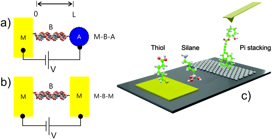 | ||
| Fig. 2 An illustration of potential molecular junction configurations. (a) M–B–A and (b) M–B–M structures, where A is an acceptor, M a metal and B a molecular bridge. In both (a) and (b) there exists a field induced potential gradient and a derived chemical potential gradient. The related capacitance is given by dV = −dμ/e and dV = e/C. A density-of-states (DOS) can be ascribed to B or to A in determining both the nature of the charge transport (conductance) and the energy storage (capacitance) of these mesoscopic elements. (c) Illustrates an AFM break junction contact as potentially applied to molecules assembled through thiol(ate), silane or pi stacking means on electronically addressable surfaces. | ||
In establishing an electronic coupling between an electrode and molecules, gold has been, by virtue of its (relative) noble character (compared, for example, to silver, which has a much lower oxidation potential) ubiquitous in the semiconductor industry, electronics and electrochemistry. It also has provided the electronic contact for much of the developments ascribed to ‘molecular electronics’. Sulfur-headgroup (primarily thiol, dithiol and disulfide motif) based organics self-assemble on gold surfaces (as well as on oxide-free Ag, Cu, Pd, Pt, Ni, Fe and also on GaAs and InP semiconductor surfaces) and represent a highly convenient mean of either passivating or actively introducing chemical functionality, such as the introduction of receptive elements for sensing, the integration of molecular motors/molecular switches, etc, or tuning distance decay parameters in tunnelling junctions. The assembly of molecules over such surfaces occurs through very accessible gas phase or (primarily) liquid environments from 10–1000 mM solutions. Adsorption times vary according to adsorbate and degree of film crystallinity sought or possible. For greater levels of alkylation, well-ordered self-assembled monolayers (SAMs) can be obtained in 2–12 hours. Derived films have been extensively analysed in the near field by atomic force (AFM) and scanning tunnelling (STM) microscopies and by bulk spectroscopic methods, including those of electrochemistry.
In coupling to oxidised or hydroxylated electrode interfaces (SiO2/Si, Al2O3/Al, TiO2/Ti, mica, glass, etc), silanes (chloro, amino or alkoxy) are commonly applied. These are attached through the formation of Si–O–Si bonds in a condensation with surface hydroxyls, generating, in an idealized way, a monolayer of siloxane. In reality this surface tethering competes with lateral cross linking, the latter being increasingly dominant if the number of surface hydroxyls is low. The lateral interactions within such films are a mix, then, of covalent and hydrogen bonding in nature (in contrast to the more compact thiolate films where dispersion forces are more typically dominant). Since the initial step in adlayer formation is silane hydrolysis, the presence of some water at the surface is, therefore, necessary to catalyse the reaction. The so generated films are, thus, sensitive to preparation method (water content of the solution, temperature or chemical vapour composition), the initial degree of surface oxidation and any post film annealing. Such films are rarely crystalline or of homogeneous monolayer in nature. Because of the relative challenge of preparing reproducible and homogeneous films by silanisation, long chain organic acid derived alternatives such as carboxylates and phosphonic acid/phosphoester tethering have been explored and shown to be promising in tethering to oxidized electronically addressable interfaces. Silicon interfaces, most specifically, those pre-treated so as to be H terminated, are readily functionalised with organic and redox-active molecular constructs using the ‘hydrosilylation route’ which exploits the reaction of Si−H surfaces with 1-alkenes or 1-alkynes by thermal induction, photochemical activation (UV light), or catalysis.6
In seeking to interface molecular adducts with carbon electrodes, especially, those derived from graphene or similar (such as carbon nanotubes), pi–pi stacking methods are useful in not only preserving the natively high levels of electron mobility, but may also be utilised in chemical doping, bandgap engineering or the introduction of chemical/biochemical functionality for downstream applications in sensing.7 In many cases the (designed or otherwise) electronic characteristics of the modified carbon adduct are analysable by STM and Raman means.8 In an alternative approach, McCreery and co-workers, have pioneered the analysis of electrodeposited diazonium salts on pyrolyzed carbon films and integrated such into junctions that facilitate many millions of current–voltage cycles without breakdown. Such work has lead, pleasingly, to tunneling distance decay parameters in line with those reported by others in different experimental configurations.9
Charge transport in molecular electronics
If one ignores issues of scale and number of contacts, molecular electronic analyses differ principally from electrochemical analyses because of the absence of an electrolyte or counterion influence. This field has blossomed during the past two decades where aromatic (pi delocalisation) versus aliphatic dithiol break junction, negative differential resistance, rectification and field-effect transistor effects at the molecular scale have all been detailed. In analysing single molecules or their two-dimensional (‘film’) assemblies, the electrical junction so created may be symmetrical (the two metal contacts being of the same material and dimension – see Fig. 1b) or not, most notably when one contact is a scanning probe junction or different material (Fig. 2c). In the case of scanning probe junctions, both force10 and electric field-effects (which can be of the order of giga volts per meter) on subsequently observed ‘molecular characteristics’ should, ideally, be considered (but are very often not). The fundamental and resolved picture of ‘electron transfer’ or ‘charge injection’ at these scales, (with single molecules or films) is largely based on quantum mechanical tunneling, with associated current densities fitted to ‘direct’, Fowler Nordheim11 or Simmons12 models across some defined barrier height and width. In specific cases (in which the length regime may also be higher >5 nm) electron flow may be ballistic (mobile electrons being effectively isolated from excitons or phonons) or hopping (phase incoherent) in nature. Conducting probe AFM and/or STM spectroscopies have further supported a generalised picture where the current flow is primarily ‘through bond’ (and thus synthetically tuneable) although direct through-space tunneling (typical of configurations shown in Fig. 1a–c and 2a, b) can contribute strongly to a degree that depends sensitively on scale and experimental configuration. Tunneling efficiencies have been mapped across a broad range of molecules, as has the importance of the thiol- or dithiol-gold contact in the electronic coupling of the organic molecules to the electrode(s), with this compared to analogues Se, CN and amine links.13 In many cases, although ultraviolet photoelectric spectroscopy analyses have indicated an absence of saturated organic molecular orbital levels within several electron-volts of the Au Fermi level, there are suggestions that HOMO (Highest Occupied Molecular Orbital) or LUMO (lowest Unoccupied Molecular Orbital) mediated tunneling is important in transport across many organic components.14Charge transport across larger one-dimensional structures (the bridge mesoscopic elements of Fig. 2) such as those presented by carbon nanotubes or semiconducting nanowires (NWs) has been of considerable interest from the perspective of potentially moving beyond traditional complementary metal-oxide-semiconductor (CMOS) platforms. Semiconducting NWs can be synthesised in high yield with uniform electronic characteristics by, for example, catalysed vapour–liquid–solid means, in either chemically homogeneous or controllably heterogeneous form. These can subsequently be (albeit often crudely) integrated in FET configurations, laid down by electron beam lithography, and measured transconductance thereafter capacitively gated. More interesting still, have been developments in the rational NW assembly (rather than drop casting or spin coating) using electric fields, microfluidic flow or Langmuir Blodgett methods. In recent years crossbar circuits have been assembled where the crossed p–n type of junction represents a prototype logic component. Because of their high carrier mobility and large surface area, semiconducting NWs have also been studied in a variety of applications besides high-performance electronics, including solar cells, biochemical or chemical sensors and on chip photonic devices.
There is, then, an extensive background (highlighting challenges but also providing a generalized picture) of molecular scale charge transport across a broad range of molecules, derived films and one-dimensional structures. Rarely, however, have capacitive analyses been integrated with charge transport or concomitantly modelled. We show below that such analyses not only report on molecular state energies but also on the rate at which charge is injected or exchanged with the electrode. Let us start by recalling the fundamentals governing electronic transport at the mesoscopic scale.
The quantum of conductance
At the mesoscopic scale,4,15 the fundamental concepts of charge transfer introduced above are not only common to both ‘dry’ (solid-state molecular electronics) and ‘wet’ (electrochemistry) environments,4,15 but are also related to the capacitance4,15,16 (in either environment). In this review, the terms ‘dry’ and ‘wet’ refer specifically to analyses made in the absence (‘dry’) or presence (‘wet’) of an electrolytic solvent. We will demonstrate that both situations are described by eqn (3) below. The field induced perturbation of electrons (whether this is formally a redox process at or a ‘conductance’ established across contacts) on a mesoscale element (a nanometre scale metal, a discrete molecule, or a molecular film) coupled to electrodes is intrinsically associated with a capacitance and an associated energy storage. To examine this further we must first theoretically link the electronic transport (conductance) through an electron channel to the chemical potential and the density-of-states. The electron channel is either a molecule spanning two electrodes (‘dry’ configuration) or a molecular element bridging between a solid electrode and a redox moiety (‘wet’ configuration).We can start by considering an appropriate length scale, L, across which a field perturbation, V, occurs; this is the spatial separation between the redox site and a metal electrode continuum (Fig. 1a and 2a, wet electrochemistry) or two continuums spanned by a molecule/1D conductor (see Fig. 1b and 2b, dry molecular electronics). The induced chemical potential difference dμ, correlates with V through dV = −dμ/e. From quantum mechanics,5 the electric current that results from this imposed dμ can be calculated as di = −dμ(eν/L)(δN/δμ), where N is the number of electron particles and ν is the velocity component (in metres per second) along length L. The bridge properties are determined by the density-of-states (δN/δμ) = 2L/hν where h is the Planck constant. For a ‘perfect’ bridge, where electron transmittance is unity, we can note that di = (2e2/h)dV, where the quantum of conductance (∼12.9 kΩ)−1 is thus obtained as17G0 = di/dV = 2e2/h.
It is important to mention here that the DOS, in the analyses above, concerns that of the bridge; the chemical potential gradient across this describes the charge transport in ‘dry’, molecular electronic configurations (Fig. 2b) through a predictable associated resistance laying in parallel (see Fig. 3(a)) to the capacitance where the rate of charge transport is described by eqn (3). In the ‘wet’ electrochemical configuration (Fig. 2(a)), we are concerned with the redox site DOS (not a bridge DOS); this lies in series with the charge transport (conductance) through a resonant transport mechanism (Fig. 3(b)) that spectroscopically reports on the heterogeneous charge transfer rate (also described by eqn (3)).
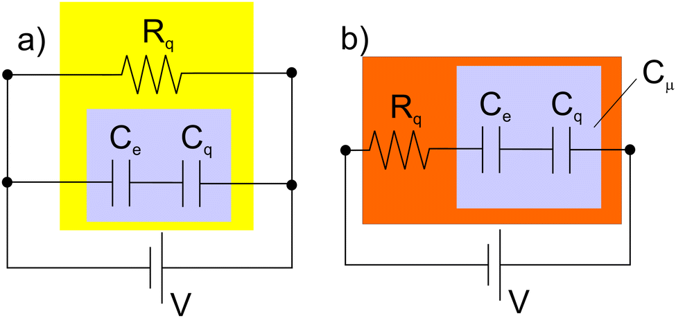 | ||
| Fig. 3 There is an intrinsic rate at which mesoscopic entities are charged under a difference of potential V as given by the relationship k = G/Cμ, a simplified form of eqn (3) where G and Cμ are combined in series or parallel. (a) Describes the equivalent circuit that applies for experimental configurations as described in Fig. 2(c) – typical of molecular electronics – and (b) for situations as described in Fig. 2(b) – typical of electrochemistry. In an ideal charge transfer situation G = 1/Rq and is associated with the quantum of resistance Rq = h/2e2. Note also that the charging current can be defined as e/τ, where the transmission time/rate are τ = RqCμ, and k = τ−1. In the case of molecular electronics e/τ corresponds to the electron transport (the electric current produced by a single electron) across the junction, whereas in electrochemistry this single electron transport is the electron transfer rate. Note that ions, solvent, and screening are modifications applicable primarily to the ‘wet’ (discussed further in Fig. 8) – electrochemical configurations.27,28 | ||
If one considers a bridge transmittance to be that produced across several channels then the conductance, G, is given by5
 | (1) |
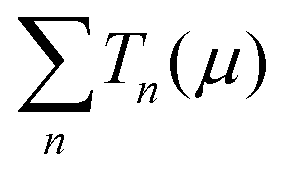 is the sum of the transmission probabilities across the molecular bridge and n is the sub-band of the transmission Tn(μ) at a given chemical potential, μ. Of course, G(μ) equates to G0 = 2e2/h when the transmission probability
  is unity for a single ideal quantum channel. Eqn (1) is general and has been applied to the conductance analysis of a broad range of molecular structures. It encompasses transport that may be tunneling, resonant or hopping in nature. For instance, in tunneling T(μ,L) is a function of μ and L such that18T(μ,L) ∝ e−βL, where β is a factor dependent on the height of the energy barrier and the nature of the medium between the states. It is useful, at this point, to note that quantised conductance,5 extensively utilised in molecular electronics, has an increasing presence in electrochemistry4,10,15,19 where it can be directly related to resolved charge transfer rates. We show below that this can also be directly related to both capacitance and specific molecular features (where the mesoscopic element is a molecule), namely the HOMO–LUMO energetics.
The mesoscopic storage of charge
In the last section we noted that dμ = −edV as the energy driving the transport of charge through a bridge connecting two states (i.e., two electrode contacts or an electrode and a mesoscopic redox-active entity). The associated field (dV) induced electronic redistribution of charge (dq) and capacitance, C, are related through 1/C = dV/dq with a stored energy E = q2/2C. In other words, this field induced energy perturbation is quantifiable as (dμ/dN) = −edV, which can be rewritten in terms of the density-of-states as (dN/dμ) = (−edV)−1. If we consider the exchange of only a single electron (dN = 1) this simplifies to dμ = −edV. This analysis demonstrates that an imposed field can induce changes in the chemical potential and thus the electronic structure (DOS) of a spanned or coupled mesoscopic entity. This is an often-ignored fact in the traditional analysis of electron transport and storage of charge at these scales.The above generated capacitance, C, is chemical or quantum in nature20 and distinct from Maxwell's electromagnetic geometric or classic/dielectric capacitance. The latter depends solely on the geometry such as C = εδ, where δ (in meters) is a geometrical parameter and ε the dielectric constant of the environment; ε = εrε0, where ε0 is the vacuum permittivity constant and εr the relative static dielectric permittivity. For instance, in a typical electronic plate capacitor model, δ is solely dependent on the length L of separation and of the area A of the plates. In electrolytic electrochemistry, this classical treatment is associated with the Debye ‘double layer’ as rationalised from statistical mechanical considerations where the geometric factor (the inverse Debye length) is quantified as δ = (e2Ni/εkBT)−1, when the capacitance is normalized per unit of area of the electrode. Here Ni is the concentration of the ions in solution, kB is the Boltzmann constant and T the absolute temperature.21 For situations where there is a potential field drop across a mesoscopic element there is, as we have noted, an additional effect [see eqn (2) below] and we must consider, then, both the geometric (coulombic forces) and chemical contributions (changes in the electronic structure) within an improved general picture of the capacitance.
Since we have established that the dμ contribution to capacitance is associated to changes in the electronic structure22 (DOS), through Density Functional Theory (DFT)22 we can correlate the field induced charge change, dq, with an index of chemical reactivity. For instance, μ for atoms and molecules, is defined exactly as the negative of Milliken's electronegativity22χ, which, in turn, correlates with ionization and affinity energies as χ = (I + A)/2. The sensitivity of dμ to the number of electronic particles (the ‘charging sensitivity’) dN, (dμ/dN) = −edV, corresponds to chemical hardness22 and its inverse, (δN/δμ) the chemical softness.22 Furthermore, it can also be noted that, any induced electron redistribution, dμ = e2/C, is proportional to the differences in the energies of the HOMO and the LUMO (Lowest Unoccupied Molecular Orbital) states.15,20,23
In summary, then, the above argues for a consideration of the field induced charge redistribution at mesoscopic scales in the generation of an associated capacitance, C, where 1/C = dV/dq and (dμ/dN) = −edV. This chemical/quantum contribution operates concomitantly with classic electrostatic capacitance during the charging of mesoscopic films (dry or wet) and we can differentiate between them using ‘e’ and ‘q’ indexes such that as Ce = εδ and Cq = e2(dN/dμ). In the next section we demonstrate that these contributions operate in series to generate a resulting electrochemical capacitance Cμ.
Unifying total capacitive contributions
This series combination of Ce and Cq (see Fig. 3) can be written as4,15 | (2) |
Eqn (2), then, represents a powerful generalised means of not only predicting both the classical and quantum mechanical limits of charge storage, but also, importantly, unifies transport in both ‘dry’ and ‘wet’ configurations (Fig. 1). In the next section we define the relationships between the quantum of conductance (and thus electron transfer rate) and this generalised electrochemical capacitance.
The rate of charge transport/transfer, quantum conductance and the electrochemical capacitance
We have above separately introduced definitions of the quantum of conductance G(μ) and electrochemical capacitance Cμ(μ). Here we show that the rate of charge transfer, injection or transport at the mesoscopic scale can be directly expressed as a ratio of these functions, G(μ)/Cμ(μ),4,15 such that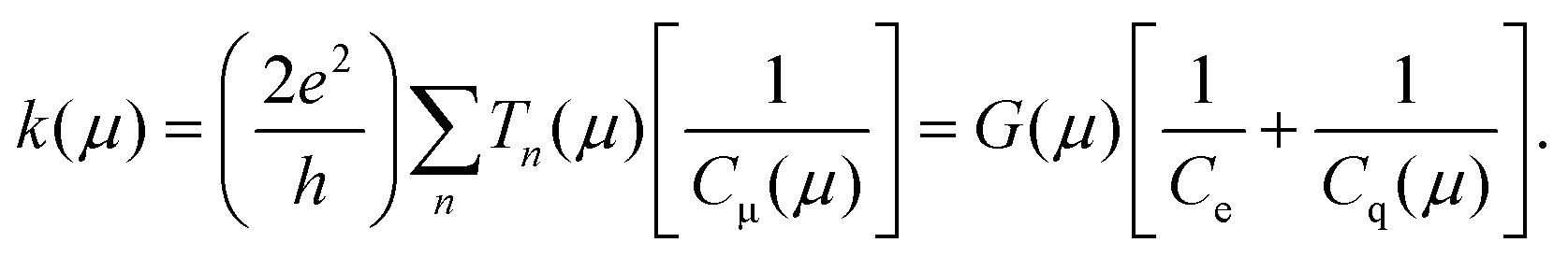 | (3) |
Eqn (3) specifically defines the time scale for electron transport/transfer processes occurring in both ‘wet’ electrochemistry and in solid-state ‘dry’16 molecular junctions. This expression is written in its zero-temperature approximation format (the temperature dependence of eqn (3) is beyond the scope of this review) and represents a unified picture consistent with Marcus's theory24 (see below). A similar association between k(μ) and the molecular conductance G(μ) has been proposed by Abrahan Nitzan25 but does not consider any capacitive contribution, field induced electronic structure perturbations, nor any aspect of the electron path chemical reactivity.4,21 Nitzan's approach25 and others10,19 have related the transmission associated with G across a molecular wire spanning two metallic electrodes proportionally with the charge-transfer rate k as measured in an analogous electrochemical configuration (where the wire spans a metallic electrode and an electrolyte exposed redox site). This has been verified for both saturated organic and nucleic acid junctions where a power-law relationship has been resolved.26 The term of proportionality between G and k has not, however, been ascribed to Cμ or anything that resembles a capacitance.
Eqn (3) confirms that the proportionality term between G(μ) and k(μ) is conveniently considered as Cμ(μ). Powerfully, both G(μ) and Cμ(μ) can be obtained experimentally from a single impedance spectroscopy measurement (see Fig. 4–13 below).
 | ||
| Fig. 4 (a) Logarithm of the modulus of current versus bias voltage for different thicknesses of azobenzene molecular films assembled between electrodes (lines denote DC and symbols AC measurements with both recorded ‘dry’ (b) corresponds to G and (c) to k (both as obtained from AC data) as functions of bias.18 | ||
 | ||
| Fig. 5 Electrochemical IS analysis of a 1.6 nm thickness redox-tagged peptide molecular film40 in ‘wet’ measurement conditions. (a) Values of Cμ measured at two different potential conditions: (red) inside and (white) outside of the faradaic window. The potential dependent contribution of Cq increases Cμ by more than two orders of magnitude within the faradaic window. In (b) the peak of the imaginary part of the capacitance as a function of frequency enables a calculation of k = G/Cμ as ∼32 Hz. The process at ∼270 Hz corresponds to the response outside the faradaic window and corresponds to k = Gs/Ct as discussed in the text. | ||
 | ||
| Fig. 6 (a) Cμ measured in a 11-ferrocenyl-undecanethiol molecular film as a function of the potential of the electrode in three different solvent environments (dielectric constants εs). Note that Cμ is related to k through eqn (3) and is solvent dependent in a Marcus’ theory manner.41 (b) Indication of the resolution of k from impedance-derived capacitive methods.42 Reprinted (adapted) from ref. 42 with permission from the American Chemical Society, Copyright (2014). | ||
 | ||
| Fig. 7 (a) Cμ, (b) G and (c) k of a 11-ferrocenyl-undecanethiol molecular film as a function of the potential of the electrode. Note that G/Cμ is in agreement with Marcus’ theory for electrode-confined41 redox species.24 Reprinted (adapted) from ref. 24, with permission from Nature, Copyright (2016). | ||
 | ||
| Fig. 8 (a) Schematic representation of quantum capacitance measurements obtained in single-layer of graphene in an electrochemical ‘wet’ configuration.43 (b) The quantum capacitance of a single graphene sheet as a function of gate potential in the configuration of (a) but measured by IS. Note that the V-shape of the capacitance as a function of gate potential is ‘equivalent’ to that obtained by Tao et al.,43 using a different methodology. | ||
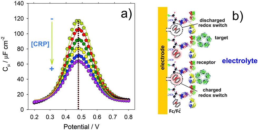 | ||
| Fig. 9 (a) The responsiveness of a redox DOS associated Cμ [∝ (dN/dμ)] to the recognition of C-reactive protein (CRP) within a mixed redox switchable and antibody constrained film. (b) Schematic representation of faradaic charging of a molecular receptive sensor. | ||
 | ||
Fig. 10 (a) Nyquist capacitive diagrams demonstrating the differences between the faradaic (dominated by Cq) and non-faradaic (dominated by Ce, in its Ct form) capacitive response of a redox active and antibody constraining molecular film to C-reactive protein (CRP). Note that (b) and (c) exhibit the real and imaginary components of the capacitance [Cμ(ω)] shown in (a). (d) Linear percentage  relative response to CRP comparing the faradaic (pseudo-capacitive) and non faradaic elements (as shown in the inset of (a) and in (d)). Reprinted (adapted) from ref. 21, with permission from Elsevier, Copyright (2016). relative response to CRP comparing the faradaic (pseudo-capacitive) and non faradaic elements (as shown in the inset of (a) and in (d)). Reprinted (adapted) from ref. 21, with permission from Elsevier, Copyright (2016). | ||
 | ||
| Fig. 11 Analytical curves indicating an assay sensitivity that is at least partially dependent on target size (a) and additionally reflective of specific receptors for a given target, here CRP, (b).46 Reprinted (adapted) from ref. 46, with permission from Elsevier, Copyright (2016). | ||
 | ||
| Fig. 12 (a) Depiction of an occupied (the minus sign denoting an anion) mesoscopic receptor-electrode interfacial (MREI) halogen bonding receptor site. (b) MREI sites coupled to the electrode. (c) These occupied sites are electronically represented by resistive-capacitive (RtCμ) serial terms15 and have an associated potential decay V = e/Cμi. (d) The responsive potential decay is from the electrode Ve to the electrolyte-exposed receptor Vi. The individual V = e/Cμi of MREI sites is modulated by an incoming (negatively) charged target which is compensated by a “mirror” (positive sign) charge in the electrode.47 Reproduced from ref. 47 with permission from the PCCP Owner Societies. | ||
 | ||
| Fig. 13 (a) Plots demonstrating the normalized variations of Cμi as a function of different ion concentrations for three different ions recruited by a halogen-bonding foldamer molecular film. Macroscopically these variations follow a Langmuir-type. (b) Corresponding plots of 1/Cμi ∝ −Δμ ∝ −eV. The blue line corresponds to a region of low ionic concentration. (c) The Hanes–Woolf linearized version of (a) plot.47 Reproduced from ref. 47 with permission from the PCCP Owner Societies. | ||
We have analysed electrochemical data sets (Fig. 1a) using eqn (3)24 and confirmed an alignment with Marcus's theory (see Fig. 6). It is instructive to note again here that the relationship between k(μ) and G(μ), is through 1/Cμ(μ) (absent from but aligned with Nitzan's insights25 as noted above). The unifying capacitive element as we have seen, contains the influence of both the dielectric of the environment through eqn (2) and of the changes in electronic structure of the electron path under field perturbation.
For those researchers with an interest in Green's function theory and methods used therein,29Cμ(μ) can be expressed as Cμ(μ) = e2(dN/dμ) = e2(1/2π)Tr[GrΓGa], where Tr is the tracer operator, Gr the retarded Green's function, Ga the self-energy of the lead connecting to the molecular system and, finally, Γ the line width describing the coupling of the lead to the electrode or another molecule. The description of (dN/dμ) here can be convenient because it allows us to model the transport properties using dynamic quantum mechanical tools in simulating explicitly how Cμ(μ) influences charge transport.
In summary, molecules coupled to electrodes under an imposed dV feel two distinct charging influences, one electrostatic and another quantized in nature, the latter directly relating to reactivity indexes through (dN/dμ). These mesoscopic charging features can be experimentally resolvable through the measurements of Cμ(μ) (see below) and additionally correlate with G(μ) and k(μ) across either the mesoscopic element (molecular electronics) or the linker between it and the electrode (electrochemistry). In next sections we focus on the applicability of G(μ), Cμ(μ), k(μ), (from now on denoted as G, Cμ, k) to a range of electronic and electrochemical configurations, together with derived applications in sensing.
The relevance of capacitance and mesoscopic concepts to conductance in solid-state molecular junctions
The above identified correlations between G, Cμ and k are, as noted, applicable in both ‘dry’ (electronic) and ‘wet’ (electrochemical) configurations as will be reinforced in this section (see also Fig. 3).By way of example, a traditional DC current–voltage analysis of ‘dry’ azobenzene films sandwiched between gold electrodes16 is compared to an IS analysis performed in the same configuration (Fig. 4); since G = i/V is resolvable by Impedance Spectroscopy (IS), we can directly resolve i as a function of applied V and then conductance and the logarithm of resolved k (the charge transport rate). These analyses demonstrate not only the ability of AC analyses to resolve the G and k elements, as defined by eqn (3) (and separately G and Cμ in a manner that is not possible by DC methods) but also an alignment of observations with those made by traditional DC analyses. It should be emphasized that this alignment requires, as is the case for ‘dry’ configurations (Fig. 1b and 2b), a consideration of a parallel relationship between G and Cμ within the scheme of eqn (3) and the equivalent circuit described in Fig. 3a.
In considering transport across molecular junctions such as these (with L up to 5 nm) the dominant transport mechanism is tunneling18,30 with an observed linear dependence of the logarithmic of k on −βL (see ref. 18) for both AC and DC measurements. We can also note a similarly resolved exponential dependence of k with applied voltage for both ‘dry’ molecular and ‘wet’ configurations,4,15,18 an indication that the kinetics of transport are aligned18,31–33 with those of charge storage, differing only in the specific relationship (series or parallel) between G and Cμ. Although IS methods have been used previously to characterize molecular junctions in ‘dry’ configurations,18 the addition of mesoscopic principles (through eqn (3)) to this analysis significantly expands our physical understanding; most notably both classical and quantum mechanical contributions to eqn (2) and (3) are considered from a chemical reactivity standpoint (see further analysis below).
We can, of course, note that charge transfer (in the electrochemical configuration) involves mobile ions, solvent, and ionic double layer responses. These are, however, additional (and separately resolvable) elements not present in ‘dry’ molecular electronics and not precluding the application of a unifying picture. Charge transport in molecular junctions may also involve thermionic emission34 and/or field ionization,35 absent in electron transfer conventional electrochemistry. These also do not interfere with the basic fundamental proposals of eqn (3) which considers universal G and Cμ components. Furthermore, the above resolved relationship between the bias dependence of k in molecular electronics (Fig. 4) is similar to that ascribed to Butler–Volmer phenomenology in electrochemistry (see Fig. 7c and sections below), reinforcing the broad applicability of the unified charge transport and storage concepts. In both situations there is an above noted exponential dependence of k on the bias voltage (or electric potential). Importantly, IS analyses (‘wet’ or ‘dry’) resolve the series or parallel relationship between G and Cμ in a manner that is interpretable (eqn (3)). In the case of the ‘dry’ (molecular electronic) configuration inter-electrode transport is through a molecular bridge such that G and Cμ are in series. For ‘wet’ electrochemical analyses, transport is resonant between the accessible redox energy states and the electrode through the molecular bridge and, although strongly influenced by the environment (solvent, ions, etc.) is still described by eqn (3) where G (through Rq) and Cμ are in series.
The electrochemistry of non-faradaic molecular films
If one presents an electrode-surface-confined and electrolyte-exposed molecule with an applied potential, V, and there exists no redox activity at V, then one would expect (only) a field driven ionic ingress.36 This can be monitored through both the resistance and capacitance of the film37,38 (which in this case is primarily ionic in nature) as measured by IS. To understand how the above discussed concepts of charge conductance G and Cμ apply here, we need to consider eqn (2) under such (ionic charging) conditions.In the absence of a molecular film, a metal/electrolyte interface can be represented by the equivalent circuit of Fig. 3(b). In this case eqn (3) applies by considering a series combination of a solution resistance Rs = 1/Gs (where Gs is the associated conductance) and double layer capacitance, Cdl. We can recall that Cdl is a particular case of Ce = εδ, and consequently, of Cμ. Considering a capacitance per unit of area of the electrode, a simple analysis gives Cdl = εδ, being δ = (e2Ni/εkBT)−1, and we can ignore Cq here because there are no accessible orbital states. If this interface is now modified with a molecular film, the response of the film to V will depend on the equilibrium concentration of the ions within the solution and their ingress into the film. This in turn is dependent on chemical potential gradients between solution and film phase ions. Under such circumstances we have a series combination of a resistance Rt = 1/Gt and a film capacitance Ct36,39 both representing the film ionic (non-faradaic) charging. Although Cdl remains resolvable it is heavily damped. The ionic Ct is separately resolved even if the film has additional faradaic activity, see Fig. 5.36,39 These (non-faradaic) resistive and capacitive terms represent, then, a fingerprint of film structure after equilibration with the electrolyte and follow the principles of eqn (3) – but in a non-faradaic fashion – where, now k = Gt/Ct, and Gt = 1/Rt and Ct (these being classical terms). Physically, this k rate reports on the dynamical dipolar relaxation response of the ions within the molecular layer to the field perturbation (and not to any electronic mobility). The nature of Ct does align with eqn (2) and the rate, Gt and Ct phenomena align with eqn (3).36,39
Electrochemical capacitance, conductance and charge transfer rate in redox molecules
In interfacing molecules with an energetically accessible redox density-of-states, dN/dμ with an electrode, a faradaic charging capacitance is resolved4,15 as Cμ in addition to the non-faradaic fingerprints referred to above (see Fig. 5). This redox contribution to (Cμ = e2(dN/dμ)) conveniently reports on k and G (Fig. 7a and b) and we can further resolve the influence of the solvent by mapping Cμ as a function of potential (Fig. 6a). We specifically see that the energetic span of accessible redox DOS is solvent dependent in accordance with the predictions of Marcus's theory of k through the associated reorganisation energy and is accordingly, dependent on the dielectric constant as shown in the inset of Fig. 6a (note that the resolved total integrated redox DOS is constant).As introduced above, we can evaluate k = G/Cμ, as a function of potential (Fig. 7) and note both that this Butler–Volmer variance (Fig. 7c) is similar to that previously presented (Fig. 4) for ‘dry’ electronic junctions, and that the peaks of G and Cμ (at the minimum value of k as shown in Fig. 7a and b) sit at the reversible redox potential.
A number of studies have applied the Nitzan approach25 (referred to above) in resolving a relationship between electrochemical k and two electrode ‘dry’ conductance G using redox tagged nucleic acids in the former case. We have ourselves4 applied capacitance spectroscopy in spectrally resolving k and Cμ and, through eqn (3), G to give values consistent with those defined by STM and single molecular conductance measurements.
The quantum capacitance of graphene
Graphene comprises a single layer of atoms with a sheet thickness of ∼0.33 nm and is, then, natively mesoscopic. Its quantum capacitance Cq has been resolved43 in wet/electrolytic configurations (see Fig. 8a). Under these circumstances, Cq has been theoretically presented as e2(m*/πħ)v(μ), where m* is the effective mass of the electron and ħ Dirac's constant.43 This interpretation is equivalent to (δN/δμ) as used here such that (δN/δμ) = (m*/πħ)v(μ), again aligning capacitance and conductance through eqn (2) and (3). This 2D-DOS,(δN/δμ) = (m*/πħ)v(μ), can be developed further44 as a function of dμ = edVG, where VG is the gate potential to provide Cq(μ) = 2e2dμ/π(ħv)2, a relationship that can be confirmed experimentally by IS. Specifically, and as shown in Fig. 8b, the bias potential dependent Cq has a minimum at the Fermi level (coinciding with the Dirac point of graphene), and increases linearly either side of this. This minimum can be understood through G = kCμ, where both G and Cμ are experimentally observed as being minimum, with Cq approaching Cμ for few graphene layers, contradicting the classical viewpoint of an antagonistic relationship between conductance and capacitance but aligning with the analysis made above for redox films (see Fig. 5 and 7 where we also note the proportionality between G and Cμ) and eqn (3).Sensors based on molecular capacitance
We have shown above that electrode confined molecules exhibit a resolvable capacitive fingerprint that tells us much about their electronic structure and, where appropriate, both the film structure (degree of ionic penetration, surface density) and the environment (dielectric). In recent work, we have shown that the local integration of receptors to the interface can lead to these capacitive signatures being utilized in derived reagentless sensors.45 The receptors may be biological or supramolecular in nature and sensing occurs through detectable localized changes in (a) faradaic activity or (b) ionic content (both changing the chemical potential of the interface). The latter is discussed below in the section “Ionic capacitive sensors”. Here we discuss (a) and start by looking at examples of biorecognition at faradaically active interfaces where (Fig. 9b), Cμ is monitored as a function of the target binding.We first note again that Cμ is dominated by the charging of accessible redox states and that Cμ = e2(δN/δμ), where (δN/δμ) represents the ‘chemical softness’ of the interface’ – the response of this DOS to an incident electric field.45 We have shown (Fig. 6a) that the distribution of this DOS is reversibly responsive to solvent dielectric. A molecular binding event, such as that occurring at a neighbouring receptive site, triggers a resolved change in occupation of this DOS (Fig. 9a). These two effects, the dispersive dielectric influence of solvent influence and DOS occupancy modulated by a local recognition event, are distinguishable.45
One can construct an analytical curve by tracking 1/Cμ as a function of target presence, where variations are linear functions of the logarithm of concentration45 (see Fig. 10d and 11), and we note that Cμ responds21 more sensitively to Cq than the much smaller, non-faradaic, Debye component, Ce, (here in its Ct non faradaic form Ct (see Fig. 5 and 10)).
Interestingly, there are some indications that the recognition induced modulation of Cμ is target dependent in a manner consistent with some contribution from Thomas Fermi screening (Fig. 11)46 such that these capacitative changes not only report on receptor governed specific targets but also contain electrostatic/electronic signatures that are specific to particular combinations of receptor and target.46 These target specific local perturbations are even more clearly resolved in the ionic binding at receptive supramolecular films (below and Fig. 11).
Ionic capacitive sensors
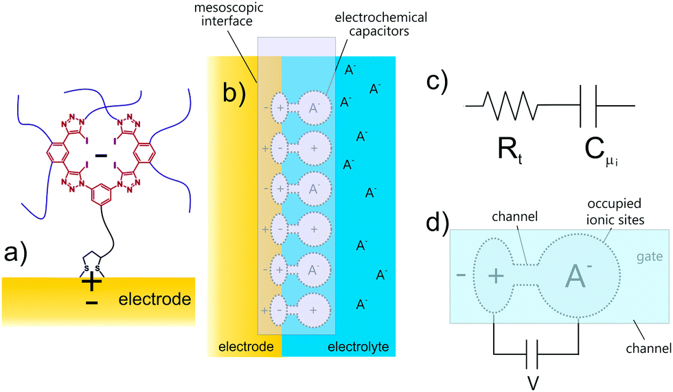
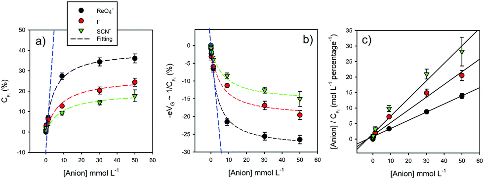
Since a detailed capacitive analysis of a molecular film can resolve a multitude of contributions, one can apply these methods to actively detecting the selective capture of ions at a designed receptive interface, that is to develop ion sensors.47,48 Traditionally, non-faradaic capacitive ion sensing has been interpreted by solely considering perturbations of a conventional double layer.49 This is a rather simplistic and incomplete picture and, furthermore, in the presence of moderately dense molecular films (see above), double layer effects are much reduced36,39 and the measured capacitance Ct, though still dominated by the Debye ‘electrostatics’, as discussed in the preceding sections, includes film characteristics itself, such as those related to non-specific ionic ingress.36,39 In an analysis of designed ion sensors we have shown that a modulation of Cμi, an ion binding specific form of Ct, (Fig. 12) follows a classic ionic Debye-type screening, where the structure of the incoming ions is unimportant and Boltzmann statistics apply (this is the linear region at low target ion concentrations <≈2 mmol L−1; blue dashed line in Fig. 12), only at low levels of ion site occupancy. In other words, Debye ‘electrostatics’ represent an approximation4,15,21 of the more general situation of eqn (2) where localized changes in electronic structure may present additional contributions to dielectric polarization, the magnitude of which will be dependent on the local chemical softness (δN/δμ) or hardness (δμ/δN). In the limit of this Thomas Fermi screening the inverse of wave vector κ−1 = (εrε0/Cμ)1/2 defines the length scale of the screening induced by the binding event46 where εrε0 is constant. Experimentally, and at higher levels of site occupancy, the capacitive response of the film to incoming ions can only be fitted by considering an appropriate electric field screening15,21 that involves exactly this. Significantly, different ions generate a different influence such that the response becomes chemical species specific.Here ion occupation follows Θ = [1 + e−βΔμi]−1 (instead of its Debye approximation, that is Θ = eβΔμi), where Δμi is the variation of the chemical potential owing to ion binding at specific recognition centres (see Fig. 12). Different ions create different electronic perturbations of the “mesoscopic element” and different associated chemical potential variations. This localized electronic structure perturbation is dependent on both specific ion charge density and the levels of site occupancy (Fig. 13) and allows for a differentiation between specific bound species; in this case the electronic structure of the halogen-bonding foldamer site responds most to the [ReO4−] ion.47
In summary, at one limit of target presence (and site occupancy) the capacitance of the interface is perturbed by induced changes in the electronic structure of the coupled film and an associated change in the V = e/Cμi dropped across it. This is a quantum mechanical effect not prior reported.
Final remarks
The integration of molecules or mesoscopic entities with electrodes lies central to a very diverse range of studies and potential applications, from analyses underpinning developments in molecular electronics, to the development of electrochemical, ionic, and biological sensors. The imposition of a V across mesoscopic structures generates a chemical potential gradient from which a derived capacitance is measurable. This capacitance, spectrally resolved through impedimetric analyses, is multi-component in nature, where signatures related to film dielectric and ionic ingress are resolvable. For interfaces that are additionally redox active, a detailed capacitive analysis enables a direct resolution of not just redox characteristics but also the associated quantum mechanical features that map directly onto the (conductance) observations of molecular electronics. This unification of ‘wet’/electrochemical and ‘dry’/molecular electronics through conductance G and electrochemical capacitance Cμ is powerful and new. A division of electron transport (electronics) and electron transfer (electrochemistry),4,15,18,50 is, to some extent, a false dichotomy reinforced by practice and nomenclature. If one ignores contact and environmental differences, a simple comparative application of the mesoscopic principles summarised here demonstrates a fundamental alignment of these areas. An underpinning principle here is the importance of the molecular hardness/softness characteristics as presented at an interface and the responsivity this gives measurable capacitance to localized electrostatic/electronic perturbations as induced by an applied field or local recognition event. An understanding of these molecular contributions should allow us to synthetically engineer better interfacial and nanoscopic sensors and to more conveniently map the charge transfer characteristics that will underpin further developments in nanoscale electronics.The concepts enshrined within eqn (3) are general and, although exemplified here with molecular films, apply equally well to single molecule or molecular wire analyses in either ‘dry’ and ‘wet’ environments.
Conflicts of interest
There are no conflicts to declare.Acknowledgements
Professor Bueno acknowledges the support of FAPESP for financial support to his research. Professor Bueno also acknowledges the individual support by CNPq provided to his head of research activities at Sao Paulo State University. The authors both acknowledge much appreciated support from The Royal Society.Notes and references
- A. L. Eckermann, D. J. Feld, J. A. Shaw and T. J. Meade, Coord. Chem. Rev., 2010, 254, 1769–1802 CrossRef CAS.
- L. A. Bumm, J. J. Arnold, M. T. Cygan, T. D. Dunbar, T. P. Burgin, L. Jones, D. L. Allara, J. M. Tour and P. S. Weiss, Science, 1996, 271, 1705–1707 CrossRef CAS.
- R. L. McCreery, Chem. Rev., 2008, 108, 2646–2687 CrossRef CAS.
- P. R. Bueno, Anal. Chem., 2018, 90, 7095–7106 CrossRef CAS.
- S. Datta, Electronic Transport in Mesoscopic Systems, Cambridge University Press, 1997 Search PubMed.
- M. R. Linford and C. E. D. Chidsey, J. Am. Chem. Soc., 1993, 115, 12631–12632 CrossRef CAS.
- V. Georgakilas, J. N. Tiwari, K. C. Kemp, J. A. Perman, A. B. Bourlinos, K. S. Kim and R. Zboril, Chem. Rev., 2016, 116, 5464–5519 CrossRef CAS.
- Z. Zhang, H. Huang, X. Yang and L. Zang, J. Phys. Chem. Lett., 2011, 2, 2897–2905 CrossRef CAS.
- A. J. Bergren, R. L. McCreery, S. R. Stoyanov, S. Gusarov and A. Kovalenko, J. Phys. Chem. C, 2010, 114, 15806–15815 CrossRef CAS.
- J. Zhao, J. J. Davis, M. S. P. Sansom and A. Hung, J. Am. Chem. Soc., 2004, 126, 5601–5609 CrossRef CAS.
- R. H. Fowler and L. Nordheim, Proc. R. Soc. London, Ser. A, 1928, 119, 173–181 CAS.
- J. G. Simmons, J. Appl. Phys., 1963, 34, 2581–2590 CrossRef.
- F. Chen, X. Li, J. Hihath, Z. Huang and N. Tao, J. Am. Chem. Soc., 2006, 128, 15874–15881 CrossRef CAS.
- Y. Q. Xue, S. Datta and M. A. Ratner, J. Chem. Phys., 2001, 115, 4292–4299 CrossRef CAS.
- P. R. Bueno, The Nanoscale Electrochemistry of Molecular Contacts, Springer, 2018 Search PubMed.
- A. Santos, U. M. Tefashe, R. L. McCreery and P. R. Bueno, Phys. Chem. Chem. Phys., 2020, 22(19), 10828–10832 RSC.
- B. J. Vanwees, H. Vanhouten, C. W. J. Beenakker, J. G. Williamson, L. P. Kouwenhoven, D. Vandermarel and C. T. Foxon, Phys. Rev. Lett., 1988, 60, 848–850 CrossRef CAS.
- A. Santos, U. M. Tefashe, R. L. McCreery and P. R. Bueno, Phys. Chem. Chem. Phys., 2020, 22, 10828–10832 RSC.
- K. H. Bevan, M. S. Hossain, A. Iqbal and Z. Wang, J. Phys. Chem. C, 2016, 120, 179–187 CrossRef CAS.
- G. J. Iafrate, K. Hess, J. B. Krieger and M. Macucci, Phys. Rev. B: Condens. Matter Mater. Phys., 1995, 52, 10737–10739 CrossRef CAS.
- P. R. Bueno, J. Power Sources, 2019, 414, 420–434 CrossRef CAS.
- R. G. Pearson, J. Chem. Sci., 2015, 117, 369–377 CrossRef.
- P. R. Bueno, G. T. Feliciano and J. J. Davis, Phys. Chem. Chem. Phys., 2015, 17, 9375–9382 RSC.
- P. R. Bueno, T. A. Benites and J. J. Davis, Sci. Rep., 2016, 6 Search PubMed.
- A. Nitzan, J. Phys. Chem. A, 2002, 105 Search PubMed.
- E. Wierzbinski, R. Venkatramani, K. L. Davis, S. Bezer, J. Kong, Y. J. Xing, E. Borguet, C. Achim, D. N. Beratan and D. H. Waldeck, ACS Nano, 2013, 7, 5391–5401 CrossRef CAS.
- D. A. Miranda and P. R. Bueno, Phys. Chem. Chem. Phys., 2016, 18, 25984–25992 RSC.
- D. A. Miranda and P. R. Bueno, J. Phys. Chem. C, 2019, 123, 21213–21223 CrossRef CAS.
- L. Berstis and K. K. Baldridge, Phys. Chem. Chem. Phys., 2015, 17, 30842–30853 RSC.
- A. J. Bergren, R. L. McCreery, S. R. Stoyanov, S. Gusarov and A. Kovalenko, J. Phys. Chem. C, 2010, 114, 15806 CrossRef CAS.
- K. J. Vetter, Electrochemical Kinetics: Theoretical and Experimental Aspects, Academic Press, 1967 Search PubMed.
- A. J. Bard and L. R. Faulkner, Electrochemical Methods: Fundamentals and Applications, John Wiley & Sons, New York, 2nd edn, 2001 Search PubMed.
- L. Yuan, L. Wang, A. R. Garrigues, L. Jiang, H. V. Annadata, M. Anguera Antonana, E. Barco and C. A. Nijhuis, Nat. Nanotechnol., 2018, 13, 322 CrossRef CAS.
- Z. Karipidou, B. Branchi, M. Sarpasan, N. Knorr, V. Rodin, P. Friederich, T. Neumann, V. Meded, S. Rosselli, G. Nelles, W. Wenzel, M. A. Rampi and F. von Wrochem, Adv. Mater., 2016, 18, 3473–3480 CrossRef.
- H. Yan, A. J. Bergren, R. McCreery, M. L. Della Rocca, P. Martin, P. Lafarge and J. C. Lacroix, Proc. Natl. Acad. Sci. U. S. A., 2013, 14, 5326–5330 CrossRef.
- J. Lehr, J. R. Weeks, A. Santos, G. T. Feliciano, M. I. G. Nicholson, J. J. Davis and P. R. Bueno, Phys. Chem. Chem. Phys., 2017, 19, 15098–15109 RSC.
- E. Boubour and R. B. Lennox, Langmuir, 2000, 16, 7464–7470 CrossRef CAS.
- E. Boubour and R. B. Lennox, Langmuir, 2000, 16, 4222–4228 CrossRef CAS.
- M. S. Goes, H. Rahman, J. Ryall, J. J. Davis and P. R. Bueno, Langmuir, 2012, 28, 9689–9699 CrossRef CAS.
- J. P. Piccoli, A. Santos, N. A. Santos, E. N. Lorenzon, E. M. Cilli and P. R. Bueno, Biopolymers, 2016, 106, 357–367 CrossRef CAS.
- C. E. D. Chidsey, Science, 1991, 251, 919–922 CrossRef CAS.
- P. R. Bueno and J. J. Davis, Anal. Chem., 2014, 86, 1337–1341 CrossRef CAS.
- J. L. Xia, F. Chen, J. H. Li and N. J. Tao, Nat. Nanotechnol., 2009, 4, 505–509 CrossRef CAS.
- T. Fang, A. Konar, H. L. Xing and D. Jena, Appl. Phys. Lett., 2007, 91 Search PubMed.
- P. R. Bueno, F. C. B. Fernandes and J. J. Davis, Nanoscale, 2017, 9, 15362–15370 RSC.
- B. L. Garrote, F. C. B. Fernandes, E. M. Cilli and P. R. Bueno, Biosens. Bioelectron., 2019, 127, 215–220 CrossRef CAS.
- P. R. Bueno, R. Hein, A. Santos and J. J. Davis, Phys. Chem. Chem. Phys., 2020, 22, 3770–3774 RSC.
- R. Hein, A. Borissov, M. D. Smith, P. D. Beer and J. J. Davis, Chem. Commun., 2019, 55, 4849–4852 RSC.
- P. R. Bueno and J. J. Davis, Anal. Chem., 2014, 86, 1337–1341 CrossRef CAS.
- R. L. McCreery, Chem. Rec., 2012, 12, 149–163 CrossRef CAS.
Footnote |
| † Professors Davis and Bueno are Founders of Osler Diagnostics, a spin-off company from the University of Oxford. |
| This journal is © The Royal Society of Chemistry 2020 |