
 Open Access Article
 This Open Access Article is licensed under a Creative Commons Attribution-Non Commercial 3.0 Unported Licence
Surface chemistry effects on work function, ionization potential and electronic affinity of Si(100), Ge(100) surfaces and SiGe heterostructures†
Ivan
Marri
 *ab,
Michele
Amato
c,
Matteo
Bertocchi‡
a,
Andrea
Ferretti
b,
Daniele
Varsano
b and
Stefano
Ossicini
abd
*ab,
Michele
Amato
c,
Matteo
Bertocchi‡
a,
Andrea
Ferretti
b,
Daniele
Varsano
b and
Stefano
Ossicini
abd
aDepartment of Sciences and Methods for Engineering, University of Modena e Reggio Emilia, 42122 Reggio Emilia, Italy. E-mail: marri@unimore.it
bCentro S3, Institute of Nanoscience—Italian National Research Council (CNR-NANO), via Campi 213/A, 41125 Modena, Italy
cUniversité Paris-Saclay, CNRS, Laboratoire de Physique des Solides, 91405, Orsay, France
dCentro Interdipartimentale En&Tech, 42122 Reggio Emilia, Italy
First published on 30th October 2020
Abstract
We combine density functional theory and many body perturbation theory to investigate the electronic properties of Si(100) and Ge(100) surfaces terminated with halogen atoms (–I, –Br, –Cl, –F) and other chemical functionalizations (–H, –OH, –CH3) addressing the absolute values of their work function, electronic affinity and ionization potential. Our results point out that electronic properties of functionalized surfaces strongly depend on the chemisorbed species and much less on the surface crystal orientation. The presence of halogens at the surface always leads to an increment of the work function, ionization potential and electronic affinity with respect to fully hydrogenated surfaces. On the contrary, the presence of polar –OH and –CH3 groups at the surface leads to a reduction of the aforementioned quantities with respect to the H-terminated system. Starting from the work functions calculated for the Si and Ge passivated surfaces, we apply a simple model to estimate the properties of functionalized SiGe surfaces. The possibility of modulating the work function by changing the chemisorbed species and composition is predicted. The effects induced by different terminations on the band energy line-up profile of SiGe surfaces are then analyzed. Interestingly, our calculations predict a type-II band offset for the H-terminated systems and a type-I band offset for the other cases.
1 Introduction
The design of novel semiconductor electronic devices often goes through the engineering of new electronic and optical properties obtained across materials manipulation at the atomic scale. In this context, functionalization by adsorption/chemisorption of atoms and molecules on semiconductor surfaces allows for tailoring new properties through charge reorganization and dipole moments modification at the surface. Indeed, an adequate choice of both substrate and covering layers, accompanied by an insightful understanding of the intrinsic factors that control orientation and magnitude of dipoles at the surface, can facilitate the realization of hybrid electronic devices for different technological fields such as optoelectronic, energy conversion, charge storage, sensing and electrochemical catalysis. Until today, the impact of the functionalization of semiconductor surfaces and the role played by coverage in both k-dispersive and low dimensional systems have been mainly studied for silicon.1–12 Nevertheless, germanium is also becoming a promising material to replace Si because of its small energy gap and its high intrinsic carrier mobility.13–18 To date, its poor oxidation properties have hindered a real practical use. Nevertheless, alternative means of surface passivation (in particular organic functionalization) specifically aimed at tuning the interface properties are now employed.19–26 In this context, particular attention has been given to the study of the work function (WF), the ionization potential (IP), and the electron affinity (EA) of functionalized surfaces. These macroscopic quantities depend on the chemistry and morphology of the surface and are sensitive to the charge reorganization that occurs after surface functionalization. These surface-related parameters are fundamental to control both charge transfer and charge transport across the interface of electronic devices and can be intentionally modified by engineering specific surface dipoles, that is by passivating semiconductor surfaces with selected atoms and molecules. WF, IP and EA are currently studied to interpret electron and hole transport in heterostructures, to investigate energy barrier at heterojunction interfaces,27–29 and to understand photoemission, thermoionic emission, absorption, photoluminescence, catalytic and carrier injection properties of electronic devices.8,30–33 In this context, the passivant surface coverage represents a further degree of freedom that can be exploited to modify and control these parameters.In the last decades WF, IP, and EA have been experimentally measured in different Si34–59 and Ge surfaces,56,59–63 by photoelectron spectroscopy, low energy electron diffraction, Kelvin probe techniques, and electrical device measurements. From a theoretical point of view, WF, IP, and EA have been often studied using ab initio schemes based on the density functional theory (DFT),59,63–74 rarely in combination with methodologies based on the Many Body Perturbation Theory (MBPT).75,76 Theoretical investigations have mainly addressed the analysis of both clean and functionalized Si surfaces, while there is a lack of studies dedicated to Ge surfaces. Among the others, Li et al.75 made a first tentative to combine LDA-DFT and GW methods to estimate the IP of thin Si(111) slabs functionalized with different groups, X = –H, –CH3, –C2H5, –Cl and –Br. Recently, Arefi et al.72 have adopted GGA-DFT to predict chemical trends in the WF of Si(111) slabs terminated with X = –I, –Br, –Cl, –I, –TeH, –SH and –OH.
In this work we combine DFT and MBPT in the GW approximation to accurately calculate WF, IP and EA of defect-free Si(100) and Ge(100) surfaces terminated with different halogens (X = –F, –Cl, –Br, or –I) and polar radicals (X = –OH or –CH3). As for functionalized Si surfaces, our work extends the analysis already performed on these materials by increasing the accuracy of the calculations. Instead, the use of the ab initio methods (and in particular of the MBPT) to calculate these quantities is a novelty for what concerns functionalized Ge surfaces. The obtained results are finally used to predict electronic properties of SiGe heterostructures and, in particular, the role played by coverage on both WF and band-edge offset. An analysis of this type, performed using ab initio state-of-the-art methods, is fundamental to design new Si, Ge and SiGe based electronic devices. Moreover, it can support experimental activities in the interpretation of experimental data, for instance concerning the study of surface chemistry (often the determination of the absorbed species and of their composition is performed using surface-sensitive techniques that lead to a direct determination of the WF, IP, and EA) and in the engineering of new devices.
The (100) surfaces of Ge and Si exhibit a variety of reconstructions mainly related to the different ordering of surface dimers. Though the most common reconstruction is the (2 × 1), here we analyze the (1 × 1) unreconstructed surfaces because, as observed in experiments, upon adsorption of atoms and molecules often the (2 × 1) reconstruction undergoes a deconstruction to the (1 × 1) configuration for both Si(100)77–79 and Ge(100)80–82 surfaces. For all the considered systems, we analyze the mechanisms that are responsible for the modulation of WF, IP, and EA. The results are compared with the ones obtained for the hydrogenated surfaces, that typically represent the starting point for the preparation of samples with different passivations.
The manuscript is organized as follows: in Section 2 we describe the theoretical approach adopted to calculate the electronic properties of X = –H, –I, –Br, –Cl, –F, –CH3 and –OH passivated Si and Ge surfaces, with special focus on WF, IP and EA. In Section 3 we report the results of the present computational investigation. In particular, in Section 3.1 we discuss the study of functionalized Si(100) surfaces while in Section 3.2 we summarize the outcomes for the X-terminated Ge(100) surfaces. In Section 3.3, starting from the WFs calculated for the single X:Si(100) and X:Ge(100) systems, we apply a simple model to estimate the WF of functionalized SiGe surfaces. We show, for the first time, the possibility of modulating this quantity on a large range of values by modifying both the Si and Ge concentration and the surface functionalization. In Section 4 we summarize the results and draw the conclusions.
2 Method
In this work we consider functionalized Si(100) and Ge(100) surfaces. Surfaces are initially modeled through the supercell method using slabs formed by 36 and 52 layers (corresponding to 36 and 52 atoms per unit cell), with a thickness of nearly 5 and 7 nm, respectively. For all the systems, a vacuum region of about 9 nm is considered.As a first step, hydrogenated systems obtained by saturating with H atoms the two dangling bonds at both the top and bottom layers of the cleaned unreconstructed slab are considered. Then, functionalized structures are obtained by replacing one of the capping H atoms with the chemical species X; the substitution is done both at the top and at the bottom of the slab in such a way to preserve both symmetry and charge neutrality of the supercell. We adopt therefore centrosymmetric slabs. This choice is made to avoid the formation of artificial electric fields (a fictitious field arises indeed when asymmetric slabs are considered83), and thus to facilitate the calculation of the WF, IP and EA. First principles calculations within DFT are performed using the plane-wave pseudopotential code PWscf of the Quantum ESPRESSO distribution.84,85 The local density approximation (LDA) for the exchange correlation functional and norm-conserving pseudopotentials (Perdew–Zunger exchange–correlation functional) are adopted for all the considered systems. Depending on the passivating species, the kinetic energy cutoff for the plane-wave basis is assumed to be 35 Ry (X = –H, –Br, –Cl, –CH3 and –I) or 65 Ry (X = –OH and –F). Atomic positions are determined by total energy minimization, assuming the in-plane lattice parameter of Si and Ge bulks, respectively. The systems are fully relaxed until the magnitude of the forces acting on each atom is converged to less than 0.003 Ry bohr−1. A 18 × 18 × 1 Monkhorst–Pack k-mesh is used to sample the first Brillouin zone.
Quasiparticle (QP) corrections, calculated using the G0W0 approximation (in the following we will just refer to GW approximation) as implemented in the MBPT code yambo,86,87 are then included to correct the Kohn–Sham (KS) eigenvalues. This step is fundamental to correctly describe band-gaps and valence band maximum (VBM) and conduction band minimum (CBM) absolute positions, and thus to correctly estimate WF, IP and EA and to produce a proper band-edge line-up between the different considered functionalized surfaces. Further computational details on the adopted GW procedure are provided in Appendix 5.1 and 5.2. By definition, the WF is the minimum energy required to move an electron from the bulk into the vacuum region across the surface, that is:
| WF = Evac − EF | (1) |
| IP = Evac − EVBM | (2) |
| EA = Evac − ECBM. | (3) |
The second approach, here named line-up potential method, is based on the procedure described in ref. 68 and 74 and can be applied only when the bulk-like character of the surface bandgap is preserved after chemisorption of atoms/molecules. Starting from a generic unrelaxed and functionalized slab formed by n layers (in our case of Si or Ge), treated in the DFT framework, the method consists of: (i) remove both passivating atoms/molecules and the vacuum region to obtain a bulk supercell (in our case Si and Ge bulk supercells, Sinbulk and Genbulk) that contains the same number of atoms of the unpassivated slab. In parallel, (ii) relax the passivated slab keeping the atomic positions of the central layers fixed (in our case the six central layers), to simulate the bulk properties of the surface. For each structure, calculate KS eigenvalues and eigenvectors and the vacuum potential in a direction perpendicular to the surface.88 Finally (iii) superimpose the oscillating planar average of the electrostatic potential calculated for the bulk supercell with the one calculated in the middle region of the passivated relaxed slab. The WF is then calculated as the difference between the vacuum energy and the EF of the bulk supercell (Sinbulk and Genbulk in our case, see Section 5.3 for more details). At the same time, IP and EA are calculated as the difference between the vacuum energy and the VBM and CBM of the bulk supercell. Within the MBPT framework, the line-up potential method is applied by modifying the VBM and CBM energies calculated within the DFT scheme by including GW corrections. We will see later that this procedure is, for our systems, the most reliable for the calculation of the WF, IP, and EA.
3 Results
We report below the results obtained in the study of WF, EA and IP for functionalized Si(100) and Ge(100) surfaces; the obtained results are then used to predict properties of terminated SiGe heterostructures.3.1 X:Si(100) surfaces: MBPT results
In this section we discuss the results obtained in the study of WF, IP, and EA for Si(100) surfaces terminated with X = –F, –Cl, –Br, –I, –OH and –CH3 groups, labelled X:Si(100) in the following. As a first step, we combine DFT and MBPT in the GW approximation to study the electronic properties of X:Si(100) slabs formed by n = 36 Si layers (X:Si(100)n=36slab). In Table 1 we report the calculated DFT-LDA (first column) and GW (second column) electronic gaps, together with the quasiparticle (QP) corrections for the VBM and CBM states (third and fourth column). The DFT band structure of the H:Si(100)36slab together with the VBM and CBM square modulus wave-function contour plots for three different passivations, that is the H:Si(100)36slab, F:Si(100)36slab and CH3:Si(100)36slab are shown in Fig. 1. Results of Table 1 point out that both DFT and GW energy gaps are almost independent on the chemiabsorbed specie and the specific functionalization is not responsible for the formation of in-gap states. As a consequence, the energy gap of defect free X-terminated Si(100) surfaces (and of large slabs that are able to well reproduce the surface properties) have to resemble the one of Si bulk. Absorption of polar and non-polar species contributes only to a charge reorganization at the adsorbate/substrate interface which modifies the electric dipole at the surface, and thus the position of the vacuum energy.| X:Si(100)n=36 | ||||
|---|---|---|---|---|
| E LDAgap (eV) | E GWgap (eV) | ΔEGWVBM (eV) | ΔEGWCBM (eV) | |
| Si36H4 | 0.559 | 1.575 | −0.813 | 0.203 |
| Si36H2F2 | 0.554 | 1.550 | −0.799 | 0.197 |
| Si36H2Cl2 | 0.552 | 1.561 | −0.803 | 0.207 |
| Si36H2Br2 | 0.550 | 1.556 | −0.803 | 0.203 |
| Si36H2I2 | 0.520 | 1.546 | −0.834 | 0.192 |
| Si36H2(OH)2 | 0.535 | 1.533 | −0.799 | 0.199 |
| Si36H2(CH3)2 | 0.566 | 1.559 | −0.796 | 0.198 |
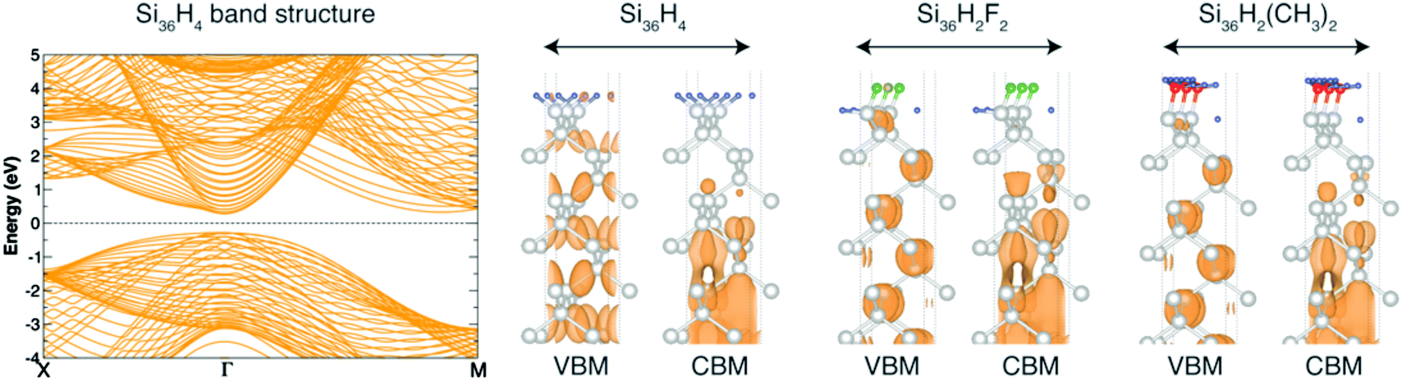 | ||
| Fig. 1 Left: DFT band structure for the H:Si(100)36slab. GW corrections open the gap of about 1 eV without affecting the band dispersion. Right: Square modulus wave-function for the VBM and CBM of H:Si(100)36slab, F:Si(100)36slab and CH3:Si(100)36slab. | ||
Due to the Brillouin zone folding, the considered slabs show a direct gap at Γ (in Fig. 1 we only report the H:Si(100)36slab case but very similar band structures are obtained for all the other systems considered). Remarkably, the calculated GW energy gaps strongly overestimate the one of the Si bulk (see Table 1). These results prove that centrosymmetric slabs formed by n = 36 Si layers are not able to correctly describe the bulk-like character of the gap region of defect-free X-terminated Si(100) surfaces. The reason is mainly related to the slow convergence of the VBM with respect to the number of layers of the slab. Fig. 1 clearly shows that the VBM is delocalized over the whole structure and therefore its properties are not determined by bulk states only (for simplicity in Fig. 1 the VBM and CBM are reported for three systems, however, our considerations, can be extended to all the structures studied here). The situation does not significantly improve when the number of layers is increased from 36 to 52; we observe, indeed, a reduction of only 0.1 eV in the calculated GW energy gap that, therefore, remains quite far from the expected bulk value. Despite surface structural properties (and in particular the relative dipole moments at the surface) are relatively weakly dependent on the slab thickness, the convergence of the electronic structure of X:Si(100) requires the use of very thick slabs.65,75,89–91
In view of the these findings, the direct method, where surface properties are directly deduced from the analysis of large slabs, is therefore not profitable for the determination of the WF, IP and EA of X-terminated (1 × 1) Si(100) surfaces.
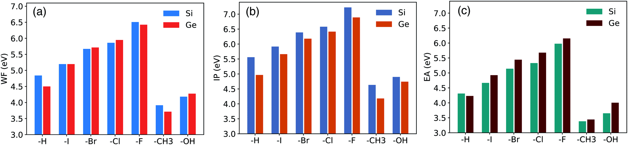
For this reason, the calculation of these parameters is here done by using the line-up potential method. By removing the inaccuracy induced by the quantum confinement of the electronic density, this method results to be the most appropriate in the present context. Remarkably, it also reduces the computational cost of the simulations because, in this case, GW corrections have to be calculated for a bulk supercell and not for a thick slab with a large quantity of vacuum. The results obtained with the above procedure are summarized in Table 2 and divided in two sub-tables. In the first part of the table we report WF, IP, and EA calculated within the DFT-LDA scheme, the surface potential shift ΔVsurf (calculated as the difference between the vacuum potential and the potential at the middle of the slab), and the z component of the electric dipole at the surface μzsurf normalized on the surface cell area. Note that DFT-LDA calculations can be exploited to identify trends in the WF, IP and EA but fail to account quantitatively for these parameters. In the second part of Table 2, we report the WF, IP and EA obtained within MBPT (GW), i.e. the values calculated by including the QP corrections for the Sin=36bulk VBM (QPVBM = −0.838 eV) and CBM (QPCBM = −0.093 eV) states. Results are also shown in Fig. 2. Remarkably, the inclusion of GW corrections mainly affects the IP while the EA remains almost unchanged with respect to the DFT-LDA case. The inclusion of GW corrections leads to an increment of about 0.37 eV with respect to the value of WF calculated at the DFT-LDA level. Electronegativity of chemisorbed atoms/molecules (ΛX) are reported in the caption. Following the procedure adopted in ref. 71 and 75, the systems reported in Table 2 can be grouped in two classes, that is surfaces passivated with non-polar groups (vanishing electric dipole moments) and surfaces passivated with polar groups (non-vanishing electric dipole moments). The systems belonging to the first class are the X = –F, –Cl, –Br, –I halogen terminated surfaces. For these structures the WF increases monotonically with increasing electronegativity of the chemisorbed specie X. This effect is a direct consequence of the higher value of ΛX with respect to ΛSi and of the absence of a net dipole moment of the adsorbate radical. As a consequence ΔVsurf (and thus WF) is only controlled by the dipole induced at the surface. The halogens produce strong, directional, monovalent bonds and generate an electron withdrawal effect from the surface whose relevance increases with increasing the linker electronegativity. This effect leads to the formation of a positive charge accumulation at the substrate and consequently to the generation of a negative electric dipole that points towards the surface. The resulting electrostatic potential hinders the movement of electrons away to the surface and leads to an increased WF. The charge redistribution generated by surface passivation is also depicted in the first two panels of Fig. 4, where, as an example, we report the charge density difference for the I:Si(100) and Cl:Si(100) surfaces. The plot has been obtained by subtracting, from the passivated system, the density of each separated sub-system (the halogen atom, the H atom, and the clean surface) keeping the atomic positions frozen. As a consequence of the electron withdrawal effect from the surface, we observe an increment of the negative charge in the region between the halogen and the Si surface. In turn, this effect is then responsible for the augmented electric dipole that generates the increased WF.
| DFT-LDA | GW corrected | |||||||
|---|---|---|---|---|---|---|---|---|
| WF (eV) | IP (eV) | EA (eV) | ΔVsurf (V) | μ z surf (a.u.) | WF (eV) | IP (eV) | EA (eV) | |
| Si36H4 | 4.470 | 4.722 | 4.218 | 0.840 | 1.843 | 4.842 | 5.560 | 4.311 |
| Si36H2I2 | 4.826 | 5.078 | 4.574 | 0.867 | 1.902 | 5.198 | 5.916 | 4.667 |
| Si36H2Br2 | 5.299 | 5.551 | 5.048 | 0.900 | 1.977 | 5.671 | 6.389 | 5.141 |
| Si36H2Cl2 | 5.489 | 5.741 | 5.237 | 0.915 | 2.008 | 5.861 | 6.579 | 5.330 |
| Si36H2F2 | 6.135 | 6.387 | 5.884 | 0.963 | 2.113 | 6.507 | 7.225 | 5.977 |
| Si36H2(CH3)2 | 3.543 | 3.795 | 3.291 | 0.772 | 1.693 | 3.915 | 4.633 | 3.384 |
| Si36H2(OH)2 | 3.810 | 4.062 | 3.558 | 0.792 | 1.738 | 4.182 | 4.900 | 3.651 |
 | ||
| Fig. 2 WF (a), IP (b) and EA (c) calculated at the GW level are reported for Si and Ge functionalized surfaces. | ||
The situation is more complicated when we consider surfaces belonging to the second class of systems, in our case X = –OH and X = –CH3. As pointed out by results of Table 2, in this case the WF does not increase monotonically with increasing electronegativity of the anchored group. For systems terminated with polar groups, μzsurf is the result of the combination of the induced dipole moment and of the non-zero moment of the surface radicals. For the cases X = –OH and X = –CH3, the overlapping of the two different electric dipole moments leads to a reduction of the μzsurf and thus of ΔVsurf and WF. A similar behaviour has been observed also for X = –OH and –CH3 terminated Si(111) surfaces.71,75,95
A direct comparison between theoretical results and experiment data is sometimes not straightforward. While potentially influenced by a number of factors (strain, defects and impurities, doping, etc.) that are difficult to control and/or model, a direct comparison between theory and experimental data is fundamental to clarify the role played by the coverage on the WF, IP and EA, as well as the relevance of crystal orientation and surface reconstruction.
A large part of the experimental data currently available concern the study of the (2 × 1) Si(111) surfaces, i.e. surfaces with a different crystal orientation and surface reconstruction with respect to the systems considered in this work. Sgiarovello et al.65 have shown that unpassivated and stoichiometric Si(100) surfaces show higher value of WF and IP with respect to Si(111) surfaces and that both WF and IP decrease when we move from ideal to reconstructed surfaces. These trends, however, have been obtained for clean non-passivated surfaces and their extension to passivated systems could be not trivial. Experiments performed on the (2 × 1) Si(100) clean surface point out values of WF ranging from 4.7 eV to 4.9 eV.34,37,39,40 The unreconstructed (1 × 1) Si(100) is expected to show higher values of WF while the chemisorption of –H atoms on the surface is expected to reduce this value.65 For the (1 × 1)H:Si(100), our calculations give a WF of 4.842 eV. Our results can also be compared with those obtained by experiments performed to evaluate the IP for –H and –CH3 terminated Si(111) surfaces. The obtained values (5.29–5.31 eV for the H-terminated surface and 4.76–4.80 eV for the CH3 terminated systems47,96,97) are similar to those calculated by us for the Si(100) surface (5.560 eV and 4.633 eV for the –H and –CH3 systems, respectively), pointing out that the major role in the determination of IP (but also of WF and EA) is played by the different chemisorbed species and not by the different surface orientation. Finally we discuss the WF measured by Pouch et al.59 for the CH3 terminated (1 × 1) Si(100) surface. This system shows the same crystal orientation and the same surface reconstruction of the ones considered by us thus allowing for a direct comparison with our results. The experimental value of the reported WF (4.08 eV) is very close to the one we calculated for the same coverage (3.915 eV). The difference of about 0.15 eV is compatible with the accuracy of the GW method.
3.2 X:Ge(100) surfaces: MBPT results
In this section we analyze the results obtained in the study of X terminated Ge(100) surfaces, labelled as X:Ge(100). As previously pointed out, there is a lack of theoretical works dedicated to the electronic properties of these systems. Following the procedure described in Section 3.1, we first investigate the electronic properties of X-terminated Ge(100) slabs formed by 36 Ge layers, namely X:Ge(100)n=36slab. Calculated DFT-LDA and GW energy gaps and QP corrections for VBM and CBM states are reported in Table 3. In Fig. 3 we report the band structure for the H:Ge(100)36slab (similar trends are obtained for all the other structures) and the VBM and CBM square modulus contour plots for the H:Ge(100)36slab, F:Ge(100)36slab and CH3:Ge(100)36slab. Differently to the Si(100) slabs, the Ge(100)36slab structures show an indirect band gap. For these systems the transition from a direct to an indirect gap occurs for slabs thinner than the ones considered by us.98–100 Similarly to the Si(100) slabs, also in this case the calculated energies gap systematically exceeds the one of the Ge bulk. As observed for the X:Si(100) surfaces, also in this case the main problem is due to the slow convergence of the band edge states with respect to the number of layers of the slab. In particular, for all the considered systems, both the VBM and CBM are delocalized over the whole structure (for simplicity we report in Fig. 3 only three systems but the same conclusions hold for all the other considered structures), that is the bulk-like region of the slab is not properly converged. A correct description of the WF, IP and EA of X:Ge(100) surfaces through the direct method requires, thus, the use of very thick slabs which are difficult to treat with methods based on the MBPT. Following the procedure described in Section 3.1, QP corrections for the VBM and CBM states are obtained by considering the Ge bulk supercell Gen=36bulk and the WF, IP, and EA are obtained by applying the line-up potential method. Calculated QP corrections for the band edge states of Ge36bulk are QPVBM = −0.627 eV and QPCBM = −0.098 eV, that lead to a GW energy gap of 0.708 eV and to an increment of 0.264 eV in the WF with respect to the DFT case. Similarly to the X:Si(100) case, the inclusion of GW corrections mainly affects the IP while the EA remains practically unchanged with respect to the value calculated within DFT. The calculated values for WF, IP, and EA are reported in Table 4. In particular in the first part of the table we report WF, IP and EA calculated within DFT-LDA (together with the ΔVsurf and μzsurf) while in the second part we report the same quantities calculated within MBPT. The latter are also reported in Fig. 2. Results of Table 4 and Fig. 2 underline trends similar to the ones obtained for the functionalized Si surfaces. For what concerns the surface passivated with halogen atoms, we observe a monotonic increment of WF, IP, and EA when increasing the electronegativity of the absorbed atom. Also in this case we observe the accumulation of a positive charge at the substrate (see for instance the last two panels of Fig. 4) and the generation of an electric dipole that points toward the surface. At the contrary, the absorption of polar groups leads to a reduction of these surface parameters. The differences with respect to the functionalized Si surfaces are therefore only related to the absolute values of WF, IP, and EA. By comparing the results of Table 2 with those reported in Table 4, we can observe that the calculated ΔVsurf and μzsurf for X:Ge(100) are always smaller than those obtained for X:Si(100). Again, we observe that the WF of Si structures are larger than those of Ge when X = –H, –I, –F, –CH3, while WF is larger for germanium surfaces when X = –Br, –Cl and –OH. At the same time the IP is always larger for the X:Si(100) surfaces, while, except for X = –H case, EA results always larger for functionalized Ge(100) surfaces.| X:Ge(100)n=36 | ||||
|---|---|---|---|---|
| E LDAgap (eV) | E GWgap (eV) | ΔEGWVBM (eV) | ΔEGWCBM (eV) | |
| Ge36H4 | 0.308 | 1.164 | −0.619 | 0.238 |
| Ge36H2F2 | 0.237 | 1.090 | −0.623 | 0.230 |
| Ge36H2Cl2 | 0.246 | 1.093 | −0.619 | 0.228 |
| Ge36H2Br2 | 0.244 | 1.092 | −0.619 | 0.229 |
| Ge36H2I2 | 0.239 | 1.094 | −0.630 | 0.225 |
| Ge36H2(OH)2 | 0.269 | 1.120 | −0.618 | 0.223 |
| Ge36H2(CH3)2 | 0.220 | 1.056 | −0.613 | 0.223 |
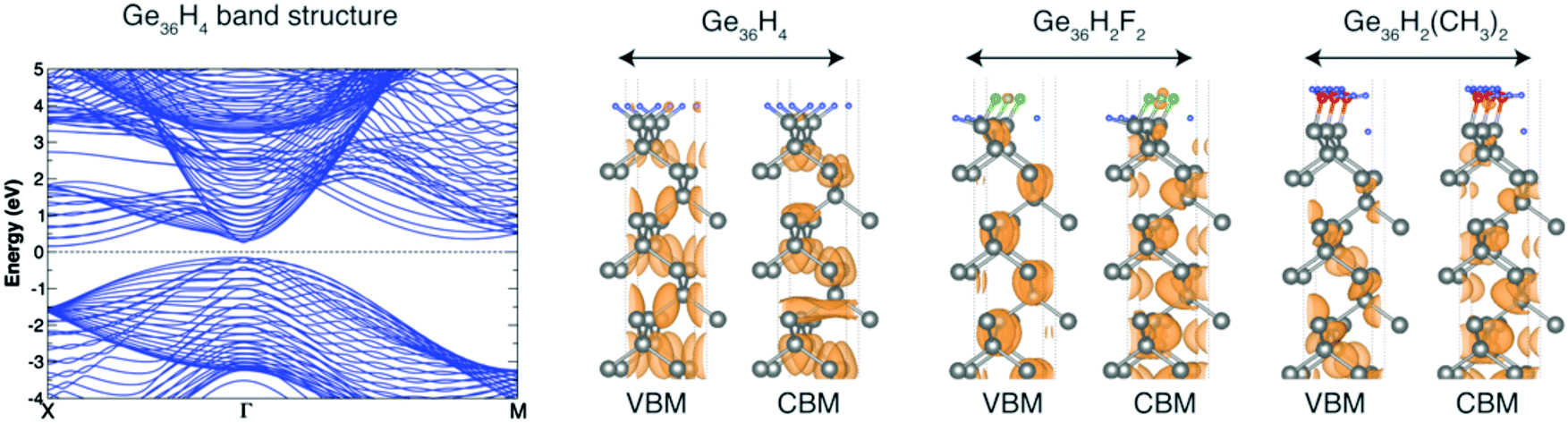 | ||
| Fig. 3 Left: DFT band structure for the H:Ge(100)36slab. GW corrections open the gap of about 0.85 eV without affecting the band dispersion. Right: VBM and CBM square modulus wave-function contour plots for the H:Ge(100)36slab, F:Ge(100)36slab and CH3:Ge(100)36slab. | ||
| DFT-LDA | GW corrected | |||||||
|---|---|---|---|---|---|---|---|---|
| WF (eV) | IP (eV) | EA (eV) | ΔVsurf (V) | μ z surf (a.u.) | WF (eV) | IP (eV) | EA (eV) | |
| Ge36H4 | 4.238 | 4.344 | 4.132 | 0.269 | 0.633 | 4.501 | 4.967 | 4.230 |
| Ge36H2I2 | 4.934 | 5.040 | 4.828 | 0.322 | 0.755 | 5.197 | 5.663 | 4.926 |
| Ge36H2Br2 | 5.451 | 5.557 | 5.345 | 0.359 | 0.843 | 5.714 | 6.180 | 5.443 |
| Ge36H2Cl2 | 5.686 | 5.792 | 5.580 | 0.376 | 0.883 | 5.949 | 6.415 | 5.678 |
| Ge36H2F2 | 6.161 | 6.267 | 6.055 | 0.411 | 0.964 | 6.424 | 6.890 | 6.153 |
| Ge36H2(CH3)2 | 3.452 | 3.558 | 3.346 | 0.211 | 0.496 | 3.715 | 4.181 | 3.444 |
| Ge36H2(OH)2 | 4.013 | 4.119 | 3.907 | 0.254 | 0.597 | 4.276 | 4.742 | 4.005 |
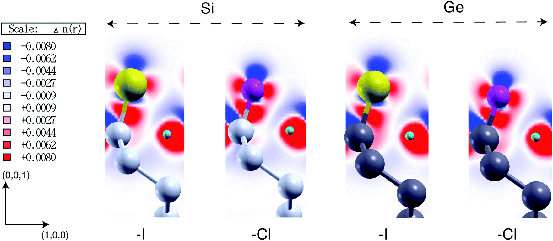 | ||
| Fig. 4 Charge density difference calculated for X = –I, and X = –Cl functionalized Si(100) and Ge(100) slabs from −0.008 to 0.008 e a0−3. An increment (decrement) of the negative charge is represented by the red (blue) colour. | ||
A direct comparison of the results of Table 4 with experiments is, also in this case, not trivial. To our knowledge, WF, IP, and EA of functionalized Ge surfaces have been investigated only in few works. These studies are mainly concerned with the analysis of reconstructed surfaces that often show a different orientation with respect to the one considered in this work. For a clean Ge(100) surface, Serino et al.26 reported a WF of 4.56 eV, while a WF of 4.67 eV was measured via UPS for the (2 × 1) Ge(100) by Walker et al.101 This value decreases by 0.33 eV (WF = 4.36 eV) upon hydrogen termination. For the (2 × 1) Ge(001) a value of WF = 4.5 eV was measured by Landermark et al.102 while values of 4.36 and 5.09 eV were reported for the EA and IP of epi-(2 × 1) Ge(001) in ref. 103. These results have to be compared to our calculated values, that for the H-terminated (1 × 1) Ge(100) surface are WF = 4.501 eV, EA = 4.230 eV and IP = 4.967 eV, respectively.
3.3 SiGe heterostructures
Combining Si and Ge to create novel heterostructures with desired properties is an appealing route to realize new devices with improved characteristics compared to traditional Si-based systems. Some properties can be deduced, as a good approximation, starting from the characteristics of the two constitutive elements. As an example, recently, Pouch and coworkers59 have measured the WF in (1 × 1) Si1−xGex(100) heterostructures as a function of the composition. For the case x = 1, the authors obtained a WF of 4.2 eV. The interpretation of this result, however, is not straightforward because the composition of the surface was not uniquely defined. In particular, the analysis performed on the sample pointed out the presence of carbon (–CH3 termination) and hydrogen (–H termination), but not their concentration. By assuming that, as a good approximation, the WF can be obtained as a linear combination of the single H:Ge(100) and CH3:Ge(100) WFs weighted by the mutual concentrations (the validity of this assumption will be discussed below), our results seem to indicate an equal concentration of H and CH3 species at the surface. Indeed, the measured WF falls almost halfway between the WF calculated for the H:Ge(100) (4.501 eV) and the one obtained for the CH3:Ge(100) (3.715 eV). More in general, it is possible to say that the WF of SiGe surfaces can be often deduced by applying a nonlinear interpolation of the WF of the constituents weighted on their concentration, where the deviation from the linearity is due to the presence of a bowing factor. In the following, on the basis of the results obtained for the Si and Ge systems and adopting simple arguments, we provide some predictions about the behaviour of SiGe heterostructures, without performing calculations on SiGe slabs. This choice is supported by the evidence that interface effects in a SiGe system mostly depend on the one-electron features of the two bulk materials considered separately.104 Furthermore, a recent model based on DFT simulations of SiGe slabs and confirmed by experiments, shows that the work function of complex SiGe alloys can be easily predicted by using a linear interpolation of the work function of the Si and Ge systems.73 Indeed, as shown in ref. 73, for SiGe heterostructures, the bowing factor is small and can be neglected without affecting too much the final result; as a consequence, the WF of X-terminated Si1−xGex surfaces can be estimated by applying the relation:| WFX:Si1−xGex = (1 − x) × WFX:Si + x × WFX:Ge | (4) |
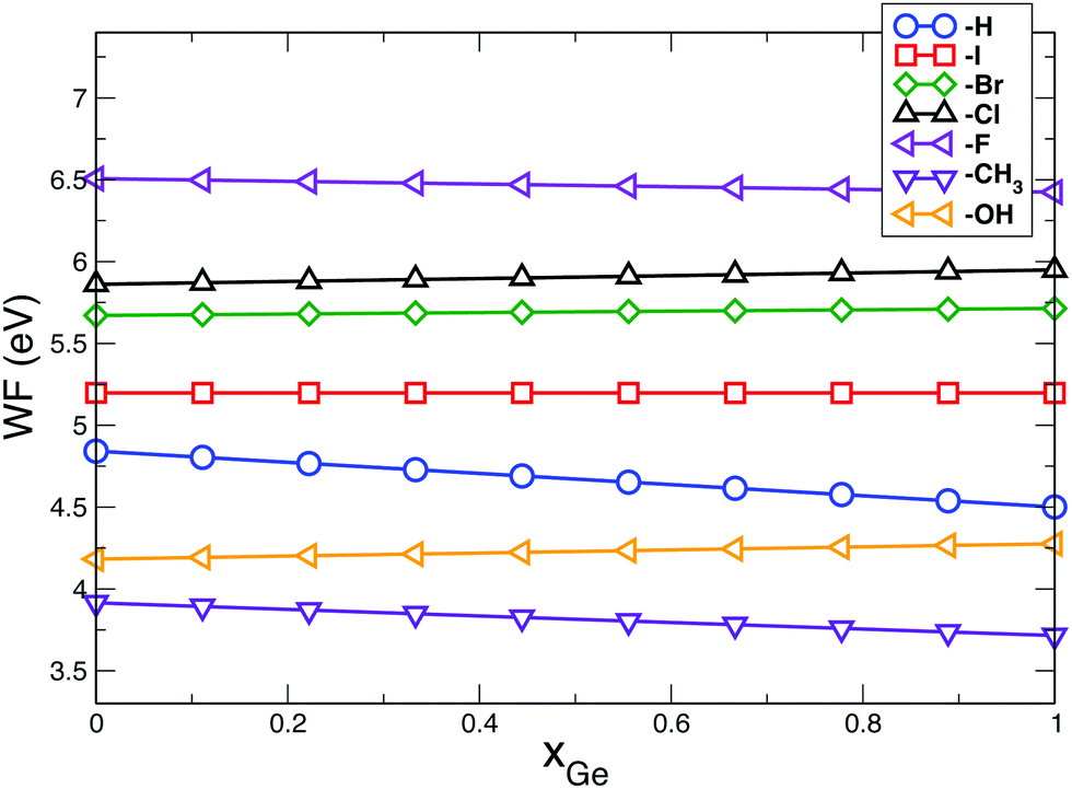 | ||
| Fig. 5 Calculated WF for X:Si1−xGex(100) surfaces as a function of the Ge concentration for different chemisorbed species. Here we consider surfaces where both Si and Ge atoms have the same termination. The other cases can be deduced starting from data of Tables 2 and 4 by using eqn (4). Effects induced by strain have been neglected. | ||
By tuning Si and Ge concentration and by modifying the surface passivation, we can therefore change the heterostructure WF. In particular, changes in the passivation can lead to variations up to 2.5 eV in the WF while the composition leads to finer variations in the order of fractions of eV. Noticeably, WF is almost independent of the Si and Ge concentration when X = –I. At the contrary, the WF decreases with increasing the Ge concentration when X = –H, –F and –CH3 while it increases with increasing the Ge concentration when X = –Cl, –Br and –OH.
Results of Tables 2 and 4 can be also used to predict effects induced by passivation on the band offset character of SiGe heterostructures of large size, that is on the band discontinuity induced by the presence of two semiconductors of different gap, EA and IP. This step is important because in the past only little attention has been dedicated to the study of the effects induced by surface coverage on the SiGe surface band offset.
Predicted offset profiles for SiGe surfaces are reported in Fig. 6. Results are obtained by aligning the band edges of the X:Si(100) and X:Ge(100) surfaces with respect to the vacuum energy (noticeably a similar approach was adopted by C. Fasolato et al.107 to predict the band alignment at the interface in polytypic Ge NWs of large diameter). Here we compare the band energy line-up calculated for H:SiGe(100) with the ones obtained for X = –I, –Br, –Cl, –F (halogens, top panel of Fig. 6) and for X = –CH3, –OH (polar molecules, bottom panel of Fig. 6). Noticeably results of Fig. 6 can be extended also to abrupt or axial6,108 NWs with large diameters, i.e. approximately in the 30–100 (or more) nm range, where quantum confinement and strain effects are negligible and the facets recover the character of an infinite surface. NWs with these diameters can be routinely grown and thus are the most relevant for technological applications. Due to the large number of atoms, these systems cannot be directly investigated within MBPT and their electronic properties have to be determined using a different strategy. Obviously, especially when low dimensional nanosystems are considered (slabs, NWs and nanocrystals), other factors as the strain, the geometry of the interface, the composition, the local chemistry and the quantum confinement of the electronic density, can affect the band offset.6,108–116 For instance, SiGe NWs of few nm of diameter can show different band-offset depending on the geometry of the NWs and on the size of the Si and Ge region, while the quantum confinement effects seem to always favour the formation of a type II offset at the interface.108,114–116 However, when the size of the system increases (i.e. when we move from SiGe slabs to SiGe surfaces), the role played by the bulk properties of the single constituents became predominant.
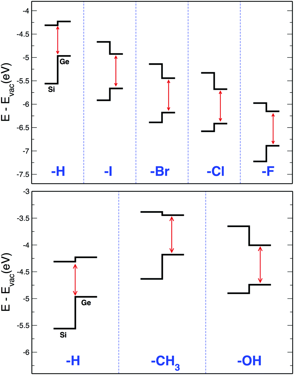 | ||
| Fig. 6 Band line-up of Si and Ge VBM and CBM calculated with respect to the vacuum energy. Only effects induced by passivations are taken into account. In low dimensional systems, these effects compete with the QC and the strain in the determination of the band-offset. | ||
Our results point out that only the case X = –H can contribute to the formation of a type II offset, with the VBM localized on the Ge atom and the CBM localized on the Si atom. Despite the band offset properties of low dimensional SiGe nanostructures are influenced by a large number of parameters (including the coverage), it is interesting to note that a type-II offset was also predicted for H-terminated abrupt SiGe NWs of few nm of diameter, with the VBM and CBM localized on the Ge and Si atoms, respectively.108 In these systems, therefore, the presence of H at the surface, as e.g. obtained when NWs are synthesized in extremely acidic conditions, contributes together with the strain and the quantum confinement to the formation of a band edge line-up where VBM and CBM are localized on different materials. At the contrary, all other passivations favour the formation of a type-I offset, with both VBM and CBM localized on the Ge atoms. In these cases, any observation of a type-II offset has to be ascribed to effects related to the strain and to the quantum confinement (this is true in particular in low-dimensional nanosystems). Despite of the lack of experimental works on such systems, these findings suggest a practical and powerful way to modulate electron and hole localizations in SiGe systems.
4 Conclusions
In this work we have calculated WF, IP, and EA of (1 × 1) Si(100) and Ge(100) surfaces terminated with X = –H, –I, –Br, –Cl, –F, –CH3, and –OH. These quantities have been evaluated within MBPT using the so-called line-up potential method. Our results point out that Si(100) and Ge(100) surfaces show very similar trends concerning WF, IP and EA. In particular, the passivation with halogen atoms always leads to an increment of the WF, IP and EA with respect to the hydrogenated system as a consequence of an electron withdrawal effect from the surface that increases together with the electronegativity of the absorbed atom. At the contrary, as a consequence of the reduction of the z-component of the electric dipole, functionalization with –CH3 and –OH groups produce a decrement in the WF, IP, and EA with respect to the –H case. For what concerns functionalized Si surfaces, our results confirm the trends obtained within the DFT scheme by other groups. The main novelty, however, consists in the application of expensive but more accurated procedures based on the MBPT within the GW approximation to calculate the absolute values (and not only the trends) of the WF, IP and EA, an important step that allows one to refine the theoretical results reported by other teams. Our approach is also a novelty for what concerns the study of WF, IP and EA for functionalized Ge surfaces, that have never been studied either in the DFT nor in the MBPT scheme. The computational determination of the absolute values of the WF, IP, and EA is fundamental to support experimental activities as well as to design new electronic devices based on functionalized Si and Ge surfaces. Starting from the results obtained for the Si(100) and Ge(100) surfaces, we have then extended our analysis to the study of SiGe heterostructures showing the possibility of both modulating the WF and controlling the band offset magnitudes by surface functionalization. In particular, we have proven that changes in the adsorbate type can lead to variations up to 2.5 eV in the WF while the tuning of the Si and Ge concentration induce finer variations, in the order of few tenths of eV. Moreover, our outcomes seems to indicate that the presence of hydrogen at the surface favour the formation of a type-II band offset with the VBM localized on the Ge atom and the CBM localized on the Si atom. At the contrary, all the other functionalization consider in this work promote the formation of a type-I offset with both VBM and CBM states clearly localized on the Ge atom. These results, which remain to be confirmed by future experimental studies, can open new perspectives in the design of novel SiGe functionalized systems with properties modeled to address specific technological needs.Author contributions
I. M., M. A., M. B. and S. O. conceived the work. I. M., M. A. and M. B. performed DFT simulations. I. M. performed GW calculations. I. M. and A. F. implemented the sum-over-state terminator techniques and D. V. and A. F. implemented the Wigner–Seitz truncation scheme into the MBPT code yambo. All authors discussed the results and implications and commented on the manuscript at all stages.Conflicts of interest
There are no conflicts to declare.5 Appendix
5.1 Computational details
Calculations have been performed adopting a simple tetragonal Bravais lattice. Band structures have been calculated considering the 2D path X (0.5, 0.0, 0.0) → Γ (0.0, 0.0, 0.0) → M (0.5, 0.5, 0.0). The electronic structure of the slabs have been determined by combining the DFT and the MBPT in the GW approximation. For both X:Si(100)36slab and the X:Ge(100)36slab both polarizability (χ) and self energy (Σ) have been converged using 1600 bands. Calculations have been performed using the SOS terminator algorithm86,117 with an extrapolar energy parameter of 1.5 Ha (see section below for details concerning this procedure). The Wigner–Seitz truncation scheme118,119 is adopted to cutoff the Coulomb interaction and thus to reduce spurious effects induced by the interaction between replicas.The absolute energy position of the VBM and CBM for both the Sin=36bulk and the Gen=36bulk have been calculated within the GW approach using the terminator scheme and imposing 500 bands for both χ and Σ and of 19 Ry for the response block size.
5.2 Sum-over-states terminators
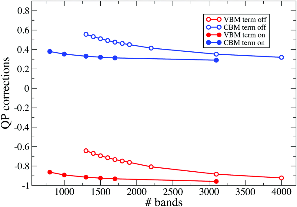
The sum-over-states (SOS) terminator method (or simply terminators) is applied to accelerate the GW calculations by reducing the number of virtual orbitals necessary to converge QP corrections. The method consists in replacing poles arising from the virtual orbitals not explicitly included in the calculation with a single extra pole, whose position is defined by the extrapolar energy parameter. This procedure leads to the truncation of the sum-over-states for both the response function (χ-term) and the self-energy (Σ-term) and improves the convergence with respect to the number of unoccupied bands, without altering the final converged results. For demonstration purposes, in Fig. 7 and 8 we report the calculated QP corrections for the VBM and CBM of the Gen=36bulk system described in a supercell. Calculations are performed with and without SOS-terminators, using a response block-size of 7 Ry.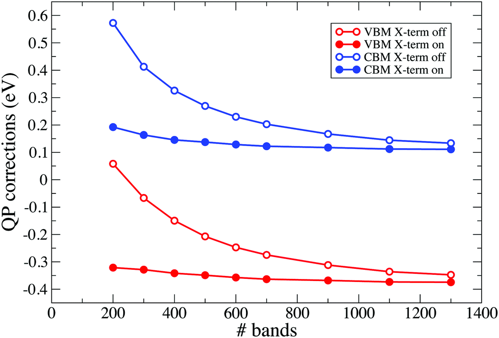 | ||
| Fig. 7 Effects of X-term on the VBM and CBM QP corrections are depicted in the figure for the Gen=36bulk described in a supercell. Terminators are applied using an extrapolar energy of 1.5 Ha. | ||
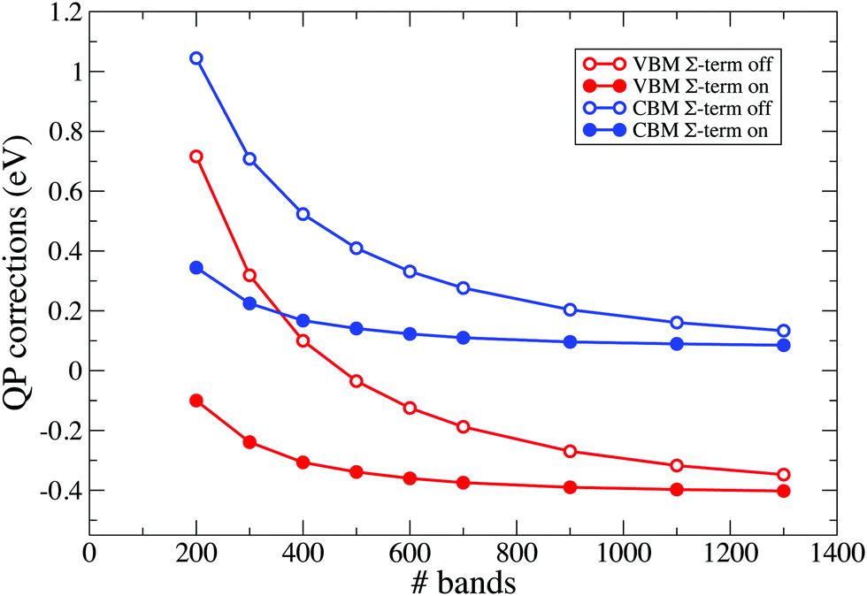 | ||
| Fig. 8 Effects of Σ-term on the VBM and CBM QP corrections are depicted in the figure for the Gen=36bulk described in a supercell. Terminators are applied using an extrapolar energy of 1.5 Ha. | ||
In Fig. 7 we report calculated QP corrections obtained by increasing the number of bands included in the calculation of the response function χ while using 1300 bands for the self-energy, that is therefore well-converged. In the figure, empty circle connected with solid lines denote QP corrections obtained without applying any correction. Results obtained by using the χ-term are denoted by solid circles connected with solid lines. In Fig. 8 we report the QP corrections calculated by adopting 1300 bands in the response function (that is therefore converged) and by increasing the number of bands in the self-energy. Also in this case, empty circle connected with solid lines denote QP corrections obtained without applying any correction while solid circles connected with solid lines represent the results obtained by adopting the Σ-term procedure. Both Fig. 7 and 8 show a relevant improvement in the convergence trends when SOS-terminators are included in the calculations. The same consideration holds for all the considered slabs. As an example, in Fig. 9 we report the QP convergences for the VBM and CBM states obtained for the H-terminated Si slabs formed by 36 layers. Results are obtained without any corrections (empty circle connected with solid lines) and by applying SOS-terminators on both χ and Σ (solid circles connected with solid lines). Corrections obtained using the standard procedure and 4000 bands for both χ and Σ can be reproduced, as a good approximation, using the terminators and about 1600 bands.
 | ||
| Fig. 9 Effects of X-term and Σ-term on the VBM and CBM QP corrections are depicted in the figure for the H-terminated Si slab. Terminators are applied using an extrapolar energy of 1.5 Ha. Results reported in the figure have been obtained by reducing to a 8 × 8 × 1 the Monkhorst–Pack k-mesh. | ||
5.3 Calculation of the WF in functionalized surfaces: the basis steps
In Section 2 we have discussed a method (the line-up potential method) to obtain, within Kohn–Sham DFT, the WF, EA and IP of a system. The procedure, applied to both the (1 × 1) Si(100) and the (1 × 1) Ge(100) surfaces, is schematized in Fig. 10, where the Ge case is analyzed. Here, EVBM and ECBM represent the top and the bottom of the Gen=36bulk valence and conduction band, respectively (dark horizontal lines). The Fermi energy for the bulk supercell is placed at midgap. Dashed and solid lines represent the planar and macroscopic average of the electrostatic potential for the different covered slabs. The electrostatic potential is calculated without including the exchange correlation contribution. The plot shown in Fig. 10 is obtained by superimposing the oscillating planar average calculated for Ge bulk and the one corresponding to the bulk-like region of the slab. In this way, we can properly align the Fermi and the vacuum energy. The separation between the Fermi energy and the vacuum energy defines the WF. IP (EA) is instead obtained by calculating the separation between EVBM (ECBM) and the vacuum energy. Finally, WF, IP, and EA are corrected by applying GW corrections to the EVBM and ECBM energies.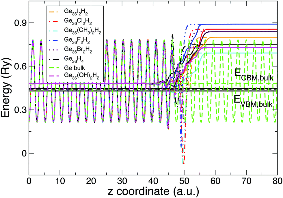 | ||
| Fig. 10 Planar (dashed lines) and macroscopic (solid line) averages of the electrostatic potential for different functionalized Ge(100) surfaces are reported in the figure. Bulk-like oscillations of functionalized slabs result independent of the absorbed molecule. In the plot they are overlapped with the one of the Ge bulk. Energies are in Rydberg. | ||
Acknowledgements
I. M. thanks the Super-Computing Interuniversity Consortium CINECA for support and high-performance computing resources under the Italian Super-Computing Resource Allocation (ISCRA) initiative, PRACE for awarding us access to resource MARCONI HPC cluster based in Italy at CINECA. I. M., A. F. and D. V. acknowledge support/funding from European Union H2020-EINFRA-2015-1 and H2020-INFRAEDI-2018-1 programs under grants agreement no. 676598 and 824143, respectively, project MaX – Materials design at the eXascale. S. O. and M. A. acknowledge support/funding from University of Modena and Reggio Emilia under project “FAR2017INTERDISC”.Notes and references
- J. M. Buriak, Chem. Rev., 2002, 102, 1271 CrossRef CAS.
- J. S. Kachian, K. T. Wong and S. F. Bent, Acc. Chem. Res., 2009, 43, 346–355 CrossRef.
- S. P. Cummings, J. Savchenko and T. Ren, Coord. Chem. Rev., 2011, 255, 1587 CrossRef CAS.
- A. V. Teplyakov and S. F. Bent, J. Vac. Sci. Technol., A, 2013, 31, 050810 CrossRef.
- K. T. Wong and N. S. Lewis, Acc. Chem. Res., 2014, 47, 3037 CrossRef CAS.
- M. Amato, M. Palummo, R. Rurali and S. Ossicini, Chem. Rev., 2014, 114, 1371 CrossRef CAS.
- W. Peng, S. M. Rupich, N. Shafiq, Y. N. Gartstein, A. V. Malko and Y. J. Chabal, Chem. Rev., 2015, 115, 12764 CrossRef CAS.
- B. Fabre, Chem. Rev., 2016, 116, 4808 CrossRef.
- S. Ossicini, O. Bisi, E. Degoli, I. Marri, F. Iori, E. Luppi, R. Magri, R. Poli, G. Cantele, D. Ninno, F. Trani, M. Marsili, O. Pulci, V. Olevano, M. Gatti, K. Gaal-Nagy, A. Incze and G. Onida, J. Nanosci. Nanotechnol., 2008, 8, 479–492 CrossRef CAS.
- R. Guerra, I. Marri, R. Magri, L. Martin-Samos, O. Pulci, E. Degoli and S. Ossicini, Phys. Rev. B: Condens. Matter Mater. Phys., 2009, 79, 155320 CrossRef.
- R. Guerra, I. Marri, R. Magri, L. Martin-Samos, O. Pulci, E. Degoli and S. Ossicini, Superlattices Microstruct., 2009, 46, 246–252 CrossRef CAS.
- I. Marri, E. Degoli and S. Ossicini, Prog. Surf. Sci., 2017, 92, 375–408 CrossRef CAS.
- D. J. Paul, Semicond. Sci. Technol., 2004, 19, R75 CrossRef CAS.
- J. Akola and R. O. Jones, Phys. Rev. B: Condens. Matter Mater. Phys., 2009, 79, 134118 CrossRef.
- S. I. Sato, T. Ohshima and M. Imaizumi, J. Appl. Phys., 2009, 105, 044504 CrossRef.
- R. L. Chu, Y. C. Liu, W. C. Lee, T. D. Lin, M. L. Huang, T. W. Pi, J. Kwo and M. Hong, Appl. Phys. Lett., 2014, 104, 202102 CrossRef.
- C. Lu, C. H. Lee, W. Zhang, T. Nishimura, K. Nagashio and A. Toriumi, J. Appl. Phys., 2014, 116, 174103 CrossRef.
- J. Sun and J. Lu, Adv. Condens. Matter Phys., 2015, 2015, 639218 Search PubMed.
- P. W. Loscutoff and S. F. Bent, Annu. Rev. Phys. Chem., 2006, 57, 467–495 CrossRef CAS.
- S. M. Han, W. R. Ashurst, C. Carraro and R. Maboudian, J. Am. Chem. Soc., 2001, 123, 2422–2425 CrossRef CAS.
- P. Ardalan, C. B. Musgrave and S. F. Bent, Langmuir, 2009, 25, 2013–2025 CrossRef CAS.
- J. S. Kachian and S. F. Bent, J. Am. Chem. Soc., 2009, 131, 7005–7015 CrossRef CAS.
- P. Ardalan, Y. Sun, P. Pianetta, C. B. Musgrave and S. F. Bent, Langmuir, 2010, 26, 8419–8429 CrossRef CAS.
- T. H. Lin, B. Y. Lin, T. Hao, H. Y. Chien, J. H. Wang and W. H. Hung, J. Phys. Chem. C, 2013, 117, 2760–2768 CrossRef CAS.
- Q. Cai, B. Xu, L. Ye, T. Tang, S. Huang, X. Du, X. Bian, J. Zhang, Z. Di, Q. Jin and J. Zhao, Appl. Surf. Sci., 2014, 316, 46–53 CrossRef CAS.
- A. C. Serino, M. E. Anderson, L. M. A. Saleh, R. M. Dziedzic, H. Mills, L. K. Heidenreich, A. M. Spokoyny and P. S. Weiss, ACS Appl. Mater. Interfaces, 2017, 9, 33592–34596 CrossRef.
- G. Ashkenasy, D. Cahen, R. Cohen, A. Shanzer and A. Vilan, Acc. Chem. Res., 2002, 35, 121–128 CrossRef CAS.
- D. Gu, R. Sistiabudi and S. K. Dey, J. Appl. Phys., 2005, 97, 123710 CrossRef.
- Y. Hirose, A. Kahn, V. Aristov, P. Soukiassian, V. Bulovic and S. R. Forrest, Phys. Rev. B: Condens. Matter Mater. Phys., 1996, 54, 13748–13758 CrossRef CAS.
- L. J. Webb, E. J. Nemanick, J. S. Biteen, D. W. Knapp, D. J. Michalak, M. C. Traub, A. S. Y. Chan, B. S. Brunschwig and N. S. Lewis, J. Phys. Chem. B, 2005, 109, 3930–3937 CrossRef CAS.
- T. R. Leftwich and A. V. Teplyakov, J. Electron Spectrosc. Relat. Phenom., 2009, 175, 31–40 CrossRef CAS.
- D. J. Michalak, S. R. Amy, D. Aureau, M. Dai, A. Esteve and Y. J. Chabal, Nat. Mater., 2010, 9, 266–271 CrossRef CAS.
- M. Hu, F. Liu and J. M. Buriak, ACS Appl. Mater. Interfaces, 2016, 8, 11091–11099 CrossRef CAS.
- G. Hollinger and F. J. Himpsel, J. Vac. Sci. Technol., A, 1982, 1, 540–545 Search PubMed.
- K. Fukiwara, Phys. Rev. B: Condens. Matter Mater. Phys., 1982, 26, 2036 CrossRef.
- A. E. Souzis, M. Sidl, W. E. Carr and H. Huang, J. Vac. Sci. Technol., A, 1989, 7, 720 CrossRef CAS.
- S. Kono, Y. Enta, T. Abukawa and T. Kinoshita, Appl. Surf. Sci., 1989, 41, 75 Search PubMed.
- V. Chakarian, D. Shuh, J. Yarmoff, M. Hakansson and U. Karlsson, Surf. Sci., 1993, 296, 383–392 CAS.
- J. Günster, T. Mayer and V. Kempter, Surf. Sci., 1996, 359, 155 CrossRef.
- Q. B. Lu, R. Souda, D. J. O'Connor and B. V. King, Phys. Rev. B: Condens. Matter Mater. Phys., 1996, 54, R17347 CrossRef.
- A. Siokou, S. Kennou, S. Ladas, T. N. Tan and J.-Y. Veuillen, Surf. Sci., 1996, 352, 628–633 CrossRef.
- T. M. Bhave and S. V. Bhoraskar, J. Vac. Sci. Technol., B, 1998, 16, 2073 CrossRef CAS.
- W. J. Royea, A. Juang and N. S. Lewis, Appl. Phys. Lett., 2000, 77, 1988–1990 CrossRef CAS.
- C. Kentsch, M. Kutschera, M. Weinelt, T. Fauster and M. Rohlfing, Phys. Rev. B: Condens. Matter Mater. Phys., 2001, 65, 035323 CrossRef.
- R. Hunger, C. Pettenkofer and R. Scheer, J. Appl. Phys., 2002, 91, 6560–6570 CrossRef CAS.
- S. Y. Davydov and A. V. Pavlyk, Tech. Phys., 2004, 49, 1050 CrossRef CAS.
- R. Hunger, R. Fritsche, B. Jaeckel, W. Jaegermann, L. Webb and N. Lewis, Phys. Rev. B: Condens. Matter Mater. Phys., 2005, 72, 045317 CrossRef.
- S. Kajita, T. Nakayama and J. Yamauchi, J. Phys.: Conf. Ser., 2006, 29, 120–123 CrossRef CAS.
- T. He, H. Ding, N. Peor, M. Lu, D. A. Corley, B. Chen, Y. Ofir, Y. Gao, S. Yitzhaik and J. M. Tour, J. Am. Chem. Soc., 2008, 130, 1699 CrossRef CAS.
- K. E. Plass, X. Liu, B. S. Brunschwig and N. S. Lewis, Chem. Mater., 2008, 20, 2228–2233 CrossRef CAS.
- L. E. O'Leary, E. Johansson, B. S. Brunschwig and N. S. Lewis, J. Phys. Chem. B, 2010, 114, 14298–14302 CrossRef.
- S. N. Novikov and S. P. Timoshenkov, Russ. J. Phys. Chem. A, 2010, 84, 1266–1269 CrossRef CAS.
- C. A. Hacker, Solid-State Electron., 2010, 54, 1657 CrossRef CAS.
- A. J. Cooper, K. Keyvanfar, A. Deberardinis, L. Pu and J. C. Bean, Appl. Surf. Sci., 2011, 257, 6138 CrossRef CAS.
- C. H. Kuo, C. P. Liu, S. H. Lee, H. Y. Chang, W. C. Lin, Y. W. You, H. Y. Liao and J. J. Shyue, Phys. Chem. Chem. Phys., 2011, 13, 15122 RSC.
- H. S. Huang, W. Y. Chan, W. B. Su, G. Hoffman and C. S. Chang, J. Appl. Phys., 2013, 114, 214308 CrossRef.
- B. Ben Hamada, A. Souissi, S. Menzli, I. Arbi, A. Akremi, C. Chefi and M. Derivaz, Thin Solid Films, 2014, 567, 96–100 CrossRef CAS.
- S. M. Nawaz, S. Dutta and A. Mallik, IEEE Trans. Electron Devices, 2015, 62, 3951–3956 CAS.
- S. Pouch, M. Amato, M. Bertocchi, S. Ossicini, N. Chevalier, T. Mélin, J.-M. Hartmann, O. Renault, V. Delaye, D. Mariolle and L. Borovik, J. Phys. Chem. C, 2015, 119, 26776 CrossRef CAS.
- L. Surnev and G. Bliznakov, Phys. Status Solidi A, 1971, 7, 75–83 CrossRef CAS.
- L. Surnev and M. Thikhov, Surf. Sci., 1982, 123, 505–518 CrossRef CAS.
- L. Surnev and M. Thikhov, Surf. Sci., 1984, 138, 40–50 CrossRef CAS.
- E. Sicilia, M. Toscano, T. Mineva and N. Russo, Int. J. Quantum Chem., 1997, 61, 571 CrossRef CAS.
- Y. Morikawa, Phys. Rev. B: Condens. Matter Mater. Phys., 1995, 51, 14802 CrossRef CAS.
- C. Sgiarovello, N. Binggeli and A. Baldereschi, Phys. Rev. B: Condens. Matter Mater. Phys., 2001, 64, 195305 CrossRef.
- A. Y. Anagaw, R. A. Wolkow and G. A. DiLabio, J. Phys. Chem. C, 2008, 112, 3780 CrossRef CAS.
- M. F. Ng, L. Y. Sim, D. X. H. Jin, K. H. Lim and S. W. Yang, Theor. Chem. Acc., 2010, 127, 689 Search PubMed.
- I. Borriello, G. Cantele, D. Ninno, G. Iadonisi, M. Cossi and V. Barone, Phys. Rev. B: Condens. Matter Mater. Phys., 2007, 76, 035430 CrossRef.
- N. E. Singh-Miller and N. Marzari, Phys. Rev. B: Condens. Matter Mater. Phys., 2009, 80, 235407 CrossRef.
- S. Hoppe, A. Michi, J. Weissmüller and S. Müller, J. Appl. Phys., 2014, 116, 073507 CrossRef.
- H. H. Arefi and G. Fagas, J. Phys. Chem. C, 2014, 118, 14346 CrossRef CAS.
- H. H. Arefi, M. Nolan and G. Fagas, Phys. Chem. Chem. Phys., 2016, 18, 12952–12963 RSC.
- M. Amato, M. Bertocchi and S. Ossicini, J. Appl. Phys., 2016, 119, 085705 CrossRef.
- M. Bertocchi, M. Amato, I. Marri and S. Ossicini, Phys. Status Solidi C, 2017, 14, 1700193 Search PubMed.
- Y. Li, L. E. O'Leary, N. S. Lewis and G. Galli, J. Phys. Chem. C, 2013, 117, 5188 CrossRef CAS.
- Y. Li and G. Galli, Phys. Rev. B: Condens. Matter Mater. Phys., 2010, 82, 045321 Search PubMed.
- J. Dabrowski and H. J. Müssig, Silicon Surfaces and Formation of Interfaces, World Scientific, 2000 Search PubMed.
- A. Papageorgepoulos and M. Kamaratos, Surf. Sci., 2000, 466, 173 CrossRef.
- X. Zhang, E. Garfunkel, Y. J. Chabal, S. B. Christman and E. E. Chaban, Appl. Phys. Lett., 2001, 79, 4051 CrossRef CAS.
- T. Weser, A. Bogen, B. Konrad, R. D. Schnell, C. Schig and W. Steinmann, Phys. Rev. B: Condens. Matter Mater. Phys., 1987, 35, 8184–8188 CrossRef CAS.
- G. W. Anderson, M. C. Hanf, P. R. Norton, Z. H. Lu and M. J. Graham, Appl. Phys. Lett., 1995, 66, 1123–1125 CrossRef CAS.
- N. Takeuchi, Surf. Sci., 1999, 426, L433–L439 CrossRef CAS.
- L. Bengtsson, Phys. Rev. B: Condens. Matter Mater. Phys., 1999, 59, 12301–12304 CrossRef CAS.
- P. Giannozzi, S. Baroni, N. Bonini, M. Calandra, R. Car, C. Cavazzoni, D. Ceresoli, G. L. Chiarotti, M. Cococcioni, I. Dabo, A. D. Corso, S. de Gironcoli, S. Fabris, G. Fratesi, R. Gebauer, U. Gerstmann, C. Gougoussis, A. Kokalj, M. Lazzeri, L. Martin-Samos, N. Marzari, F. Mauri, R. Mazzarello, S. Paolini, A. Pasquarello, L. Paulatto, C. Sbraccia, S. Scandolo, G. Sclauzero, A. P. Seitsonen, A. Smogunov, P. Umari and R. M. Wentzcovitch, J. Phys.: Condens. Matter, 2009, 21, 395502 CrossRef.
- P. Giannozzi, O. Andreussi, T. Brumme, O. Bunau, M. B. Nardelli, M. Calandra, R. Car, C. Cavazzoni, D. Ceresoli, M. Cococcioni, N. Colonna, I. Carnimeo, A. D. Corso, S. de Gironcoli, P. Delugas, R. A. DiStasio, A. Ferretti, A. Floris, G. Fratesi, G. Fugallo, R. Gebauer, U. Gerstmann, F. Giustino, T. Gorni, J. Jia, M. Kawamura, H.-Y. Ko, A. Kokalj, E. Küçükbenli, M. Lazzeri, M. Marsili, N. Marzari, F. Mauri, N. L. Nguyen, H.-V. Nguyen, A. O. de-la Roza, L. Paulatto, S. Poncé, D. Rocca, R. Sabatini, B. Santra, M. Schlipf, A. P. Seitsonen, A. Smogunov, I. Timrov, T. Thonhauser, P. Umari, N. Vast, X. Wu and S. Baroni, J. Phys.: Condens. Matter, 2017, 29, 465901 CrossRef CAS.
- D. Sangalli, A. Ferretti, H. Miranda, C. Attaccalite, I. Marri, E. Cannuccia, P. Melo, M. Marsili, F. Paleari, A. Marrazzo, G. Prandini, P. Bonfà, M. O. Atambo, F. Affinito, M. Palummo, A. Molina-Sánchez, C. Hogan, M. Grüning, D. Varsano and A. Marini, J. Phys.: Condens. Matter, 2019, 31, 325902 CrossRef CAS.
- A. Marini, C. Hogan, M. Grüning and D. Varsano, Comput. Phys. Commun., 2009, 180, 1392–1403 CrossRef CAS.
- In our approach the vacuum potential is calculated by considering, far from the surface, the planar average of the electrostatic potential in the slab supercell.
- A. Aliano, Y. Li, G. Cicero and G. Galli, J. Phys. Chem. C, 2010, 114, 11898–11902 CrossRef CAS.
- K. Sagisaka, J. Nara and D. Bowler, J. Phys.: Condens. Matter, 2017, 29, 145502 Search PubMed.
- P. Scherpelz and G. Galli, Phys. Rev. Mater., 2017, 1, 021602 CrossRef.
- A. Allred, J. Inorg. Nucl. Chem., 1961, 17, 215–221 CrossRef CAS.
- H. Chermette, J. Comput. Chem., 1999, 20, 129–154 CrossRef CAS.
- J. Mullay, J. Am. Chem. Soc., 1985, 107, 7271–7275 CrossRef CAS.
- M.-F. Ng, L. Y. Sim, H. Da, H. Jin, K. H. Lim and S.-W. Yang, Theor. Chem. Acc., 2010, 127, 689–695 Search PubMed.
- S. Maldonado, K. E. Plass, D. Knapp and N. S. Lewis, J. Phys. Chem. C, 2007, 111, 17690–17699 CAS.
- B. Jaeckel, R. Hunger, L. J. Webb, W. Jaegermann and N. S. Lewis, J. Phys. Chem. C, 2007, 111, 18204–18213 CAS.
- E. G. Barbagiovanni, D. J. Lockwood, P. J. Simpson and L. V. Goncharova, Appl. Phys. Rev., 2014, 1, 011302 Search PubMed.
- A. N. Kholod, S. Ossicini, V. E. Borisenko and F. Arnaud d’Avitaya, Surf. Sci., 2003, 527, 30–40 CrossRef CAS.
- X. K. Wu, W. Q. Huang, Z. M. Huang, C. J. Qin, T. G. Dong, G. Wang and Y. L. Tang, Chin. Phys. B, 2017, 26, 037302 CrossRef.
- M. Walker, M. Tedder, J. D. Palmer, J. J. Mudd and C. F. McConville, Appl. Surf. Sci., 2016, 379, 1–7 CrossRef CAS.
- E. Landemark, C. J. Karlsson, L. S. O. Johansson and R. I. G. Uhrberg, Phys. Rev. B: Condens. Matter Mater. Phys., 1994, 49, 16523 CrossRef CAS.
- Y. T. Cheng, Y. S. Lin, W. S. Chen, K. Y. Lin, C. P. Cheng, H. H. Cheng, J. Kwo, M. Hong and T. W. Pi, Appl. Phys. Express, 2017, 10, 075701 CrossRef.
- L. Colombo, R. Resta and S. Baroni, Phys. Rev. B: Condens. Matter Mater. Phys., 1991, 44, 5572 CrossRef CAS.
- A. A. Williams, J. M. C. Thornton, J. E. Macdonald, R. G. van Silfhout, J. F. van der Veen, M. S. Finney, A. D. Johnson and C. Norris, Phys. Rev. B: Condens. Matter Mater. Phys., 1991, 43, 5001–5011 CrossRef CAS.
- M. Amato, M. Palummo and S. Ossicini, Phys. Status Solidi B, 2010, 247, 2096–2101 CrossRef CAS.
- C. Fasolato, M. De Luca, D. Djomani, L. Vincent, C. Renard, G. Di Iorio, V. Paillard, M. Amato, R. Rurali and I. Zardo, Nano Lett., 2018, 18, 7075–7084 CrossRef CAS.
- M. Amato, M. Palummo and S. Ossicini, Phys. Rev. B: Condens. Matter Mater. Phys., 2009, 80, 235333 CrossRef.
- C. G. Van de Walle and R. M. Martin, J. Vac. Sci. Technol., B, 1985, 3, 1256–1259 CrossRef CAS.
- C. G. Van de Walle, J. Vac. Sci. Technol., A, 2003, 21, S182–S190 CrossRef CAS.
- C. G. Van de Walle and R. M. Martin, Phys. Rev. B: Condens. Matter Mater. Phys., 1986, 34, 5621–5634 CAS.
- F. A. Reboredo, A. Franceschetti and A. Zunger, Phys. Rev. B: Condens. Matter Mater. Phys., 2000, 61, 13073–13087 CAS.
- F. Foieri, M. J. Sánchez, L. Arrachea and V. A. Gopar, Phys. Rev. B: Condens. Matter Mater. Phys., 2006, 74, 165313 CrossRef.
- M. Amato, M. Palummo and S. Ossicini, Phys. Rev. B: Condens. Matter Mater. Phys., 2009, 79, 201302 CrossRef.
- M. Amato, S. Ossicini and R. Rurali, Nano Lett., 2011, 11, 594–598 CrossRef CAS.
- M. Amato, R. Rurali and S. Ossicini, J. Comput. Electron., 2012, 11, 272–279 CrossRef CAS.
- F. Bruneval and X. Gonze, Phys. Rev. B: Condens. Matter Mater. Phys., 2008, 78, 085125 CrossRef.
- C. A. Rozzi, D. Varsano, A. Marini, E. K. U. Gross and A. Rubio, Phys. Rev. B: Condens. Matter Mater. Phys., 2006, 73, 205119 CrossRef.
- S. Ismail-Beigi, Phys. Rev. B: Condens. Matter Mater. Phys., 2006, 73, 233103 CrossRef.
Footnotes |
| † Electronic supplementary information (ESI) available. See DOI: 10.1039/d0cp04013d |
| ‡ Present address: Applied Materials Italia Srl, Via Ruini, 74/L, 42122 Reggio Emilia (RE), Italy. |
| This journal is © the Owner Societies 2020 |