
 Open Access Article
 This Open Access Article is licensed under a
 Creative Commons Attribution 3.0 Unported Licence
Saturation profile based conformality analysis for atomic layer deposition: aluminum oxide in lateral high-aspect-ratio channels†
Jihong
Yim‡
 a,
Oili M. E.
Ylivaara‡
b,
Markku
Ylilammi
c,
Virpi
Korpelainen
b,
Eero
Haimi
a,
Emma
Verkama
a,
Mikko
Utriainen
b and
Riikka L.
Puurunen
*ab
a,
Oili M. E.
Ylivaara‡
b,
Markku
Ylilammi
c,
Virpi
Korpelainen
b,
Eero
Haimi
a,
Emma
Verkama
a,
Mikko
Utriainen
b and
Riikka L.
Puurunen
*ab
aDepartment of Chemical and Metallurgical Engineering, Aalto University School of Chemical Engineering, Kemistintie 1, Espoo, Finland. E-mail: riikka.puurunen@aalto.fi; Tel: +358 50 337 8161
bVTT Technical Research Centre of Finland, PL 1000, 02044 VTT, Finland
cEspoo, Finland
First published on 30th September 2020
Abstract
Atomic layer deposition (ALD) raises global interest through its unparalleled conformality. This work describes new microscopic lateral high-aspect-ratio (LHAR) test structures for conformality analysis of ALD. The LHAR structures are made of silicon and consist of rectangular channels supported by pillars. Extreme aspect ratios even beyond 10![[thin space (1/6-em)]](https://www.rsc.org/images/entities/char_2009.gif) 000:1 enable investigations where the adsorption front does not penetrate to the end of the channel, thus exposing the saturation profile for detailed analysis. We use the archetypical trimethylaluminum (TMA)–water ALD process to grow alumina as a test vehicle to demonstrate the applicability, repeatability and reproducibility of the saturation profile measurement and to provide a benchmark for future saturation profile studies. Through varying the TMA reaction and purge times, we obtained new information on the surface chemistry characteristics and the chemisorption kinetics of this widely studied ALD process. New saturation profile related classifications and terminology are proposed.
000:1 enable investigations where the adsorption front does not penetrate to the end of the channel, thus exposing the saturation profile for detailed analysis. We use the archetypical trimethylaluminum (TMA)–water ALD process to grow alumina as a test vehicle to demonstrate the applicability, repeatability and reproducibility of the saturation profile measurement and to provide a benchmark for future saturation profile studies. Through varying the TMA reaction and purge times, we obtained new information on the surface chemistry characteristics and the chemisorption kinetics of this widely studied ALD process. New saturation profile related classifications and terminology are proposed.
A. Introduction
Conformality refers to the ability to coat a three-dimensional object with a homogeneous coating of uniform thickness.1,2 Conformal coatings are required in the fabrication of state-of-the-art and future electronics,2–4 as well as in various applications related to heterogeneous catalysts,5–8 biosensors,9 and energy industries.10,11 Atomic layer deposition (ALD),12–15 a variant of chemical vapor deposition (CVD), was invented independently over forty years ago under the names atomic layer epitaxy16–19 and molecular layering.20–22 The Millennium Technology Prize was awarded to ALD's Finnish inventor, Tuomo Suntola in 2018.23 ALD is gaining increasing interest as the method of choice for conformal thin film growth.1,2 The unique features of ALD are the systematic use of self-terminating gas–solid reactions and precise film thickness control at subnanometer level.13,14,24 When the gas–solid reactions are completed, they stop by themselves. This adsorption control results in the unparalleled conformality of ALD films.1,25–27Despite the inherent advantage of ALD, the conformal coating of a certain aspect ratio (AR) is not guaranteed.1,8,28 Thus, the tuning of ALD process parameters is needed to achieve a homogeneous coating in high-aspect-ratio (HAR) structures.1,29–31 For an ideal ALD process, the penetration depth of a coating is known to scale with the square root of the reactant dose, where the dose equals partial pressure of reactant multiplied by exposure time.29,32–34 The reactivity of the compounds, often described by a (lumped) sticking coefficient cA (A stands for Reactant A), further influences the speed at which uniform thickness is attained.1,31,35,36 Non-ideal reactions, such as unwanted CVD through decomposition of one of the reactants or through the mixing of reactant pulses, or non-saturation of the reactions, would compromise the conformality.1,37
A practical industry standard of conformality measurements has been vertical HAR (VHAR) structures etched into silicon. Scanning or transmission electron microscopy (SEM or TEM) images acquired after careful specimen preparation allow the film thickness and step coverage (ratio of the film thickness at the bottom of a feature to film thickness at the top of the feature) to be determined.1,2,29,34,35,38 Sometimes, the (lumped) sticking coefficient has been extracted from the (often sparse) data.35
As an alternative to VHAR, lateral HAR (LHAR) structures have emerged. Fig. 1 illustrates the concept of conformality analysis with LHAR channels. By removing the roof of the channel after ALD, the film is exposed for top-view analysis by methods suitable for planar surfaces. Most often, LHAR structures are intentionally fabricated with such demanding aspect ratios that the film does not reach the end of the features, which enables analysis of what we call the saturation profile of the ALD process.
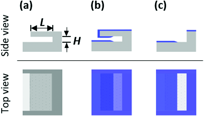 | ||
| Fig. 1 Schematic illustration of the conformality analysis with LHAR channels: (a) uncoated channel, (b) channel after ALD coating, and (c) channel after removing the roof and exposing the surface for analysis. H is the height and L the length of the LHAR channel. The illustration is intentionally not in scale: typical aspect ratios L:H in LHAR structures are at least 200:1 and the ratios in this work are typically up to 10000:1. | ||
Various types of LHAR structures appear in the literature. For example, Dendooven et al.31,39 assembled macroscopic LHAR structures with a rectangular channel, and the channel height in the hundreds of micrometers. Gao et al.40 microfabricated LHAR cavities expanding from elongated circles with single-crystal silicon at the bottom, polysilicon as the roof, and silicon dioxide pillars supporting the structure; the design cavity height was 200, 500, or 1000 nm and the ARs above 10000:1. We will refer to the structures by Gao et al.40 as PillarHall-1 (from PillarHall™, 1st generation). In turn, Schwille et al.30,41 fabricated centrosymmetric LHAR cavities resembling structures used in microelectromechanical systems (MEMS) processing; here, the limiting gap height was 4.5 μm. Recently, building upon the process of Gao et al.,40 improved microscopic rectangular LHAR channels have been developed and used, but not yet described in detail;33,36,42–44 describing them is among the goals of this work. LHAR structures have been employed to study the conformality of an emerging small minority of the more than 700 published ALD processes;45 Al2O3 from Me3Al (TMA) and H2O;30,31,33,36,40,46 TiO2 from TiCl4 and H2O;40 Ir and IrOx from Ir(acac)3 and various reactants;47 HfSiOx from Hf[N(CH3)(C2H5)]4, SiH[N(CH3)2]3, and O3;42 SiO2 from SiH2[N(CH2CH3)2]2 and O3;41 plasma enhanced ALD (PEALD) of Al2O3 and AlN from TMA, and O2 and NH3 plasma;39 and PEALD of SiO2, TiO2, Al2O3 and HfO2 from SiH2(N(C2H5)2)2, Ti(N(CH3)2)4, TMA and HfCp(N(CH3)2)3 and O2/Ar plasma.44,48
Common to LHAR approaches has typically been to measure the saturation profile of the ALD process and to extract kinetic information of the film growth through modelling.1 Often, a model is assuming either reversible or irreversible single-site Langmuir adsorption (A + * ⇌ A*) to describe an ALD reaction step, and the (lumped) sticking coefficient for the reaction is extracted from fitting a model to the saturation profile.30,31,33,36 For example, Dendooven et al.31 extracted the sticking coefficient of TMA on Al2O3 and studied its effect on step coverage with LHAR features. They also combined LHAR studies with a Monte Carlo algorithm to study the conformality of Al2O3 and AlN by PEALD.39 Schwille et al.30,41 determined the sticking coefficient of TMA and bis-diethyl aminosilane (BDEAS) by using a Monte Carlo process simulation and data obtained with LHAR features. Ylilammi et al.33 extracted the lumped sticking coefficient of TMA on Al2O3 and TiCl4 on TiO2 using a diffusion-reaction model of ALD saturation profile over LHAR features. Arts et al.36 extracted, by using LHAR features, the lumped sticking coefficient directly from the slope of the saturation profile and the recombination probability of O2 plasma radicals during PEALD of various oxides from the PEALD film's penetration depth.44
This work aims to create a benchmark for saturation profile based conformality analysis of ALD processes with microscopic LHAR structures. We chose the archetypical TMA–water process13,15,49—at the ALD temperature most typically employed for it, 300 °C— as a test vehicle for the saturation profile analysis development, because this process is known as a near-ideal ALD process,13–15 because this process has already been studied with LHAR structures,30,31,33,36,40,46 and because the details of the surface chemistry and kinetics of this process continue to be the subject of scientific investigations and debate.13,50–57 The repeatability and reproducibility of the saturation profile measurement are assessed. New information is obtained on the surface chemistry and chemisorption kinetics of the TMA–water process as a function of TMA dose and purge times. New saturation profile related classifications and terminology are developed, with applicability beyond this work. We hope that once the practicalities and limitations of the saturation profile analysis are well described for this TMA–water process, conformality studies of other ALD processes—and even of other thin film processes such as CVD and atomic layer etching (ALE)—can be compared and contrasted against this benchmark.
B. Saturation profile terminology
This section develops and discusses terminology related to saturation profiles before entering into experimental details.First, we propose a general classification of saturation profile types in LHAR features, as in Fig. 2. Examples are provided where these four classes have been used in the literature; combinations of classes have also been used. The as-measured saturation profile is obtained directly from the measurement with a measure of the total growth as the vertical axis and distance as the horizontal axis (Fig. 2a). Dendooven et al.39 and Ylilammi et al.,33 for example, used an as-measured saturation profile to present the effect of process parameters on the conformality of PEALD and ALD.
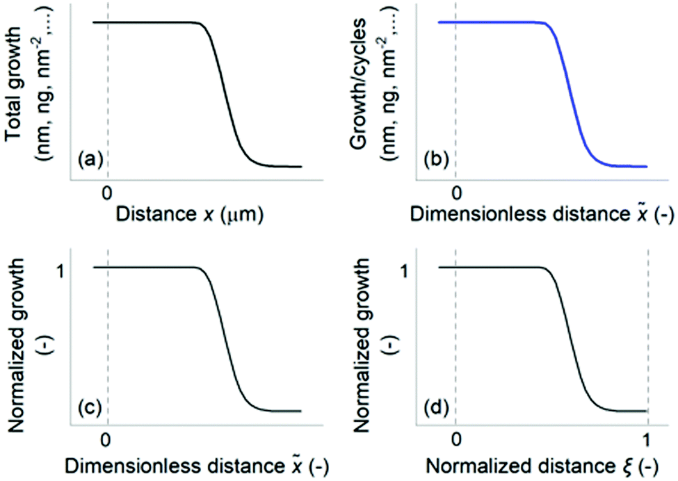 | ||
Fig. 2 Summary of the proposed saturation profile classification: (a) as-measured saturation profile, (b) scaled saturation profile, (c) Type 1 normalized saturation profile (![[x with combining tilde]](https://www.rsc.org/images/entities/i_char_0078_0303.gif) = x/H), and (d) Type 2 normalized saturation profile (ξ = x/L). = x/H), and (d) Type 2 normalized saturation profile (ξ = x/L). | ||
The scaled saturation profile has the total growth divided by cycles as the vertical axis and the measurement distance x divided by the channel height H as the horizontal axis (Fig. 2b). We call the distance scaled this way the dimensionless distance ( = x/H). Earlier, AR has often been used as the horizontal axis in a way analogous to the dimensionless distance used in this article.1,2,40,47 Advantageously, this dimensionless distance is a well-defined physical quantity that remains constant irrespective of the extent of growth, while the AR experienced by the ALD process increases during the process with increasing film thickness through narrowing of the channel.
The scaled saturation profile can be further normalized in (at least) two distinct ways. The Type 1 normalized saturation profile (Fig. 2c) has the amount of growth at channel entrance normalized to one (optionally, this value is interpreted as surface coverage θ,32,36 having values 0 ≤ θ ≤ 1) as the vertical axis and the dimensionless distance as the horizontal axis. Arts et al.36 developed a method to determine a lumped sticking coefficient directly from the slope of the Type 1 normalized saturation profile, provided that certain conditions prevail during the ALD process (most importantly, that the molecule's mean free path λ is significantly larger than the limiting channel dimension, and the so-called excess number32 is below 0.1). The Type 2 normalized saturation profile (Fig. 2d) has the distance x divided by the LHAR channel length L as horizontal axis. We call the distance normalized this way the normalized distance ξ (ξ = x/L).32 Yanguas-Gil et al.32,58 have used the Type 2 normalized saturation profile to develop criteria comparing diffusion-limited and reaction-limited ALD growth.
Second, we divide the saturation profile into four characteristic regions, as in Fig. 3a. The regions are developed to discuss the results of this work and should be applicable to other works, as well. Region I refers to the part of the saturation profile located outside, in front of the LHAR channel. Thus, this region corresponds to measurements on planar substrates, without HAR features. Region II refers to the part of the saturation profile located inside the LHAR channel, where the measured film thickness is (roughly) constant due to saturated ALD reactions. Region II starts at the entry to the LHAR channel, where the measurement distance is zero, and extends up to a knee [Fig. 3b (1)], whereafter film thickness decreases. Ideally, in Regions I and II, thickness divided by cycles gives characteristic growth per cycle (GPC) of ALD. In Region III after the knee, film thickness decreases due to non-saturated reactions. Region III can also be called an adsorption front. Region IV is located after the adsorption front; here, the film thickness should ideally be zero.
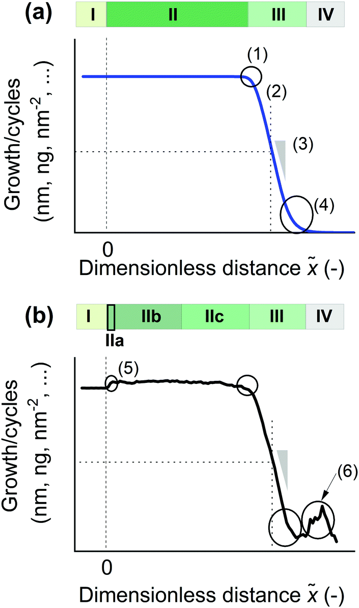 | ||
| Fig. 3 Saturation profile region classification and terminology, as used in this work for (a) the ideal simulated scaled saturation profile and (b) the experimental scaled saturation profile (experimental data for Al2O3 ALD). Region I is located outside the LHAR channel. Region II begins at zero, at the LHAR channel entry, and this region indicates the area where the film thickness is roughly constant. Typically, after a recognizable knee (1), strong decrease in film thickness starts, characteristic for Region III. Further indicated are: (2) the 50% thickness penetration depth PD50% (x50%), (3) the slope of the adsorption front at PD50%, and (4) the leading edge of the adsorption front. Region II is further divided into subregions: between Regions IIa and IIb, a nanostep (5) is sometimes experimentally observed. Division from Region IIb to IIc is made on the basis, where the total growth divided by cycles is initially at maximum. In Region IV, the film thickness should be zero, but (6) spikes were occasionally observed in experimental saturation profile data. | ||
Region II is further divided into subregions a, b, and c (Fig. 3b). Some experimental thickness measurements (including those of this work) show what we call a nanostep between Region IIa and IIb, where the measured thickness increases slightly [Fig. 3b (5)]. Region IIb refers to the early part of Region II after the nanostep, where the total growth divided by cycles is as its maximum value corresponding to saturated ALD reactions. Region IIb can be useful e.g. for modelling purposes. Region IIc refers to the rest of Region II before an observable knee in the saturation profile. (The transition from Region IIb to IIc may sometimes be somewhat arbitrary.)
C. Experimental
A. Fabrication of conformality test chips
The conformality test chip prototypes reported in this work with all-silicon LHAR channels (Fig. S1, ESI†) were produced with MEMS processing techniques using a process modified from Gao et al.40 (PillarHall-1). The test chip prototypes of this work are identified as PillarHall™ 3rd generation, or PillarHall-3, in short. Starting substrates were low-doped 150 mm silicon (100) wafers. The process encompassed typically thermal silicon oxide layer growth to the targeted channel height H (100, 500, or 2000 nm); polysilicon membrane deposition from silane (SiH4) in multiple steps; several photolithography steps; a plug-up process;40 and HF vapor etching as the final fabrication step. Wafers were optionally diced to the 15 × 20 mm chip size. The processing for a distance indicator scale on top of the membrane for optical analysis was an optional step (Fig. S2, ESI†). Thermal oxidation and polysilicon deposition were made with Centrotherm E1200 HT 260-4 furnaces, and HF etching with Primaxx MEMS-CET HF vapor etcher. Contact lithography was made with a SUSS Mask aligner MA150 and stepper lithography with a Canon FPA3000-i4 (i-line) Wafer stepper.The conformality test chip prototypes have various LHAR channels with ARs up to 10000:1, when the lateral length L is 5000 μm, and the targeted channel height is 500 nm (Table S1, ESI†). The conformality chip layout details and pillar layout designs are included in the ESI.†
B. Atomic layer deposition
ALD Al2O3 films were grown at 300 °C in a Picosun R-150 ALD reactor. The target thickness was typically ca. 50 nm made in 500 ALD cycles. The process pressure was ca. 3 hPa. Nitrogen (purity 6.0) with a constant flow rate of 150 sccm was used as the carrier and purge gas through four reactant lines. Similar to earlier studies,33,40,51 a TMA-purge-water-purge sequence (s) of 0.1–4.0–0.1–4.0 was typically used. The pyrophoric TMA was handled inertly. The samples and the experimental variables used are listed in Table 1.| Seriesa | Sample codeb | Pulse-purge sequence (s) | Design channel height Hf (nm) | Pillar layout | ALD cycles N | Reflectometer magnification | Thickness outside SI (nm) | Initial thickness SIIbc (nm) | S I/N (GPCI) (nm) | S IIb/N (GPCIIb) (nm) | x 50% (PD50%) (μm) |
50% (−) |
Sloped
|
Slope
|
Linear fitting residual R2 |
|---|---|---|---|---|---|---|---|---|---|---|---|---|---|---|---|
| a Different pillar layout design for Series A; reflectometer magnification for Series B; design channel height for Series C; ALD cycles for Series D; TMA pulse time for Series E; and purge time for Series F. b Original traceable sample codes in ESI, Table S3. c Initial film thickness SIIb was calculated as the average of the first five data points from the constant film thickness region (Region IIb, Fig. 3). For the 100 nm channel height, the initial thickness is the first data point in a constant thickness region. The optically measured thickness includes the thickness of the native silicon oxide. d The slope of the adsorption front (Region III of Fig. 3) was extracted from the scaled saturation profile by finding the best-linear fitting line. e For the design channel height H of 100 nm, the film thickness outside the channel (Region I of Fig. 3) was not measured. f For each design channel height H, the thickness of the film coated on channels having different lateral lengths L (0.1 to 5 mm) were measured several times and averaged except for the Series B for which L of 5 mm data was used. Design aspect ratio of each channel is listed in Table S1 (ESI). | |||||||||||||||
| A | 1 | 0.1-4.0-0.1-4.0 | 500 | v1a | 500 | ×50 | 49.8 | 53.3 | 0.100 | 0.107 | 140 | 280 | −0.0013 | −0.013 | 0.983 |
| 2 | 0.1-4.0-0.1-4.0 | 500 | v1b | 500 | ×50 | 49.6 | 54.5 | 0.0993 | 0.109 | 140 | 280 | −0.0013 | −0.011 | 0.991 | |
| 3 | 0.1-4.0-0.1-4.0 | 500 | v2a | 500 | ×50 | 50.5 | 53.4 | 0.101 | 0.107 | 110 | 220 | −0.0018 | −0.018 | 0.997 | |
| B | 4 | 0.1-4.0-0.1-4.0 | 500 | v1b | 500 | ×50 | 47.4 | 47.8 | 0.0949 | 0.0956 | 105 | 208 | −0.0018 | −0.019 | 0.993 |
| 5 | 0.1-4.0-0.1-4.0 | 500 | v1b | 500 | ×10 | 49.1 | 50.0 | 0.0983 | 0.100 | 103 | 208 | −0.0015 | −0.015 | 0.998 | |
| 6 | 0.1-4.0-0.1-4.0 | 500 | v1b | 500 | ×5 | 51.4 | 52.9 | 0.103 | 0.106 | 109 | 214 | −0.00087 | −0.0083 | 0.998 | |
| C | 7 | 0.1-4.0-0.1-4.0 | 100 | v1b | 500 | ×50 | —e | 47.8 | — | 0.0955 | 10 | 100 | −0.00048 | −0.0050 | 0.995 |
| 8 | 0.1-4.0-0.1-4.0 | 500 | v1b | 500 | ×50 | 46.7 | 51.1 | 0.0934 | 0.102 | 106 | 214 | −0.0020 | −0.019 | 0.993 | |
| 9 | 0.1-4.0-0.1-4.0 | 2000 | v1b | 500 | ×50 | 45.3 | 48.8 | 0.0906 | 0.0976 | 375 | 188 | −0.0046 | −0.047 | 0.995 | |
| D | 10 | 0.1-4.0-0.1-4.0 | 500 | v1b | 250 | ×50 | 24.3 | 26.0 | 0.0970 | 0.104 | 115 | 230 | −0.0022 | −0.021 | 0.982 |
| 8 | 0.1-4.0-0.1-4.0 | 500 | v1b | 500 | ×50 | 46.7 | 51.1 | 0.0934 | 0.102 | 106 | 214 | −0.0020 | −0.019 | 0.993 | |
| 11 | 0.1-4.0-0.1-4.0 | 500 | v1b | 1000 | ×50 | 94.7 | 99.3 | 0.0947 | 0.0993 | 95 | 190 | −0.00099 | −0.010 | 0.996 | |
| E | 12 | 0.1-4.0-0.1-4.0 | 500 | v1b | 500 | ×50 | 47.5 | 50.2 | 0.0951 | 0.100 | 96 | 192 | −0.0021 | −0.021 | 0.971 |
| 13 | 0.2-4.0-0.1-4.0 | 500 | v1b | 500 | ×50 | 48.2 | 49.8 | 0.0962 | 0.100 | 133 | 266 | −0.0014 | −0.014 | 0.996 | |
| 14 | 0.4-4.0-0.1-4.0 | 500 | v2a | 500 | ×50 | 48.6 | 51.0 | 0.0972 | 0.102 | 197 | 386 | −0.00045 | −0.0044 | 0.996 | |
| F | 15 | 0.1-1.0-0.1-1.0 | 500 | v1b | 500 | ×50 | 50.4 | 51.9 | 0.101 | 0.104 | 99 | 198 | −0.0017 | −0.016 | 0.983 |
| 12 | 0.1-4.0-0.1-4.0 | 500 | v1b | 500 | ×50 | 47.5 | 50.2 | 0.0951 | 0.100 | 96 | 192 | −0.0021 | −0.021 | 0.971 | |
| 16 | 0.1-10.0-0.1-10.0 | 500 | v1b | 500 | ×50 | 44.8 | 48.9 | 0.0897 | 0.0978 | 109 | 218 | −0.0017 | −0.018 | 0.999 | |
To study the effect of the pillar density on the saturation profile, Al2O3 films were coated in LHAR channels with different pillar designs of layout v1a, v1b, and v2a (design channel height: 500 nm), which had been fabricated on the same silicon wafer. Table S2 and Fig. S3 (ESI†) report the detailed information on different pillar designs. All of the films were grown in the same ALD run to avoid run-to-run variations (Series A in Table 1).
C. Characterization methods
In this work, the ALD Al2O3 film was characterized after peeling off the top membrane with adhesive tape, as shown in Fig. 1c, unless stated otherwise. Optical microscopy was routinely used to image the coated LHAR channels, before and after peeling off the top membrane with adhesive tape.Scanning electron microscopy (SEM) with energy-dispersive X-ray spectrometry (EDS) was performed using a Tescan Mira3 SEM fitted with a Thermo Scientific EDS. An accelerating voltage of 5 keV was used for the SEM-EDS line scan. The sample with the design channel height of 500 nm had been stored in ambient air. Thus, no sample preparation for charging prevention was required. Elemental X-ray mapping of the sample surface was performed first. Subsequently, line scans of elemental profiles were measured. The length of the line was 500 μm with measurement points at 1 μm intervals. Outliers due to pillars and edges in surface channels were removed from the elemental profile results. The line scans are averages of five measurements.
The surface topography was measured by using a PSIA XE-100 atomic force microscope (AFM). Non-contact mode and standard types of AFM tips were used in the measurements. The measurement area varied from 10 μm × 10 μm to 90 μm × 90 μm, and resolution was 1024 × 256 pixels. Sample tilt and drift in slow scan direction were corrected using line wise first order polynomial fit.
The saturation profiles of ALD Al2O3 films were measured by a spectroscopic reflectometer line scan (FilmTek 2000M wavelength range of 380 to 800 nm). The line scans began outside the channel in Region I of Fig. 3 (ca. 13 μm before channel entry). The total scan length was 198 or 398 μm with a step of 2 μm, and 100 to 200 data points were obtained. If not otherwise stated, a 50× objective lens with an estimated spot size of 5–6 μm was used. To study the effect of spot size on the saturation profile, 10× and 5× objective lenses with an estimated spot size of 25 and 50 μm, respectively, were used. To analyze the repeatability of the measurement at one location and within-chip reproducibility, the reflectometry measurements were repeated several times on each of the lateral lengths (pillar layout v1b). The thickness of the films coated on LHAR channels having different lateral lengths L (0.1 to 5 mm) was measured several times. Then we excluded outliers and averaged the thickness except for the Series B in Table 1 for which L of 5 mm data was used. This method gave us more representative results than treating single thickness scans.
D. Saturation profile simulation
A series of simulations was performed using a MATLAB implementation of the diffusion–reaction model developed by Ylilammi et al. 2018.33 In the simulated conditions, the mean free path1 of TMA λTMA is ca. 40 μm. The partial pressure of Reactant A was calculated with the discretized approximate solution to the one-dimensional diffusion equation, presented in eqn (17)–(28) in ref. 33. An additional simplification was made in the calculation of the gas phase diffusion constant of Reactant A (eqn (3) in ref. 33), where the collision rate of molecules at location x and time t was replaced with the collision rate of molecules at location x at the previous time step, t−1. The discretized partial differential equation describing the surface coverage as a function of time and location, eqn (31) in ref. 33 was solved with the MATLAB® ODE23 ordinary differential equation solver, where the relative tolerance was set to 10−3 and the absolute tolerance was specified at 10−5. During the implementation, a mistake was found in the original article, both terms on the right side of eqn (1) in ref. 33 should be multiplied by Avogadro's number.D. Results
A. Microscopic analysis of the coated area
Fig. 4 presents optical microscopy images of ALD Al2O3 coated LHAR channels. The top membrane was removed before the analysis. The color difference reveals the coated area. For the pillar layouts v1a and v1b (Fig. 4a and b), a penetration depth of ca. 140 μm from the channel entry was visually determined. A straight adsorption front was observed parallel to the channel entry. Pillar layout v2a (Fig. 4c) showed a wavy adsorption front and a smaller penetration depth of ca. 100 μm. The smaller penetration depth most likely originated from the top membrane hanging lower between the pillars; the hanging membrane likely resulted in a narrower channel than the target. Fig. S4 (ESI†) shows the saturation profiles for different pillar layout designs. For layouts v1a and v1b, saturation profiles overlapped. Similar to the previous microscopy results, a lower penetration depth was also observed for layout v2a. | ||
| Fig. 4 Optical microscopy images of the top view of LHAR channel with a channel length L of 1 mm and (a) pillar layout v1a, (b) layout v1b, and (c) layout v2a (samples 1, 2, and 3 in Table 1, respectively). 500 cycles of Al2O3 ALD (brown color) were grown on them at 300 °C. The notation for Regions I–IV is shown in Fig. 3. | ||
Fig. 5a presents an SEM image of the Al2O3 ALD-coated LHAR channel surface (top view of sample 11 in Table 1) with an overlayer of corresponding Al-Kα X-ray count map. The elemental mapping shows the spatial distribution of Al. The result reveals a ca. 125 μm penetration of the Al2O3 film under the top membrane (Fig. S5, ESI†). Fig. 5b presents a SEM-EDS line scan of the same sample. With the acceleration voltage of 5 kV, the interaction volume of X-rays in the sample exceeded the thickness of the Al2O3 film. Therefore, the Si signal from the substrate is seen throughout the line scan. The intensities of Al, O, and Si change as a function of distance, reflecting the film thickness profile. In front of the LHAR channel (Region I of Fig. 3b), at a range of ca. −40 to 40 μm (Fig. 5b), a constant film thickness was observed. Subsequently, a plateau continued with slightly increased film thickness (Region II b and II c, Fig. 3b). After a knee point, the thickness decreased sharply to zero.
 | ||
| Fig. 5 (a) SEM image of sample 11 surface (top view) with an overlayer of corresponding Al-Kα X-ray count map in red. 1000 growth cycles were used on the LHAR channels with a design height of 500 nm (sample details are reported in Table 1). (b) SEM-EDS line scans of elemental profiles for Al, Si, and O in the same sample. The notation for Regions I–IV in Fig. 3. | ||
Fig. 6 shows an AFM image of LHAR channel sample surface coated by Al2O3 ALD. The white parts and black parts indicate top membrane remnants and pillar footprints, respectively. Near the channel entry, a nanostep is visible, at which the surface roughness begins (Region IIa of Fig. 3b). A curtain-shaped waviness was observed from this region (moving from Region IIa to IIb). The nanostep was detected in the AFM line scan (Fig. S6, ESI†).
 | ||
| Fig. 6 AFM image of the LHAR channel (design channel height of 500 nm) coated by an Al2O3 film at 300 °C in 500 cycles (sample details at Table S4, ESI†). The notation for Regions I–II in Fig. 3. The top membrane was removed with adhesive tape. Remaining membrane remnants are seen in white and holes left by ripped off pillars in black. | ||
B. Effect of spot size on the measured saturation profile
Fig. 7 shows the as-measured saturation profile for different spot sizes of the reflectometer measurement. The higher the magnification used, the smaller the spot size. As the spot size increased, the bump created by membrane remnants at the channel entry broadened. In addition, the adsorption front became enlarged. The results show that the shape of the measured saturation profile depends on the measurement spot size when the spot size is larger than the width of the adsorption front. Thus, the smallest spot size of 5 μm (×50), clearly smaller than the width of the adsorption front (ca. 30 μm), was used henceforth to measure the saturation profiles. | ||
| Fig. 7 As-measured saturation profiles for ALD Al2O3 as a function of reflectometer spot sizes. Samples 4, 5, and 6 (Table 1 Series B). | ||
C. Repeatability and reproducibility of saturation profiles
Fig. 8a presents the repeatability of reflectometer measurement and within-chip reproducibility demonstrated using LHAR channels with the design channel height of 500 nm and various lateral lengths L. Corresponding results for the design heights of 100 and 2000 nm are presented in Fig. S7 (ESI†). The overlapping saturation profiles showed good measurement repeatability. The saturation profiles with different lateral lengths overlapped. This result suggests that the lateral length of the LHAR channel has no significant impact on the saturation profile measurement, at least in the studied case of Al2O3 ALD. | ||
| Fig. 8 Repeatability of saturation profile measurement (a) for ALD Al2O3 film grown on a LHAR channel (sample 8 in Table 1) and reproducibility of ALD runs (b) for Al2O3 films made in 500 cycles on various LHAR channels, having the same design channel height of 500 nm and pillar design of v1b. Sample details are in Table 1. | ||
Fig. 8b compares results of different chips, ALD runs, and times, where the ALD parameters were kept constant. Different chips showed somewhat different film thickness and penetration depth although the same ALD sequence had been employed. Small differences in the pressure in the ALD runs, reflectometer measurements, and the actual channel height compared to design values are among the uncertainty sources as discussed in more detail in Section E.
D. Effect of the channel height and film thickness on the saturation profiles
Fig. 9 (panels a–c) presents the effect of the channel height on the saturation profile of Al2O3 ALD (Table 1, Series C). A constant thickness region (Region II of Fig. 3) was observed for design heights of 500 and 2000 nm. The larger the channel height, the deeper the film penetrated (Fig. 9a). The scaled and normalized saturation profiles of the samples in 500 and 2000 nm channels practically overlap, while for a channel height of 100 nm, the adsorption front began with no preceding constant thickness region. The scaled and normalized saturation profile of the sample with a 100 nm channel height differed from the series because the 100 nm channel entry was plugged by a ca. 50 nm thick film as the ALD process proceeded.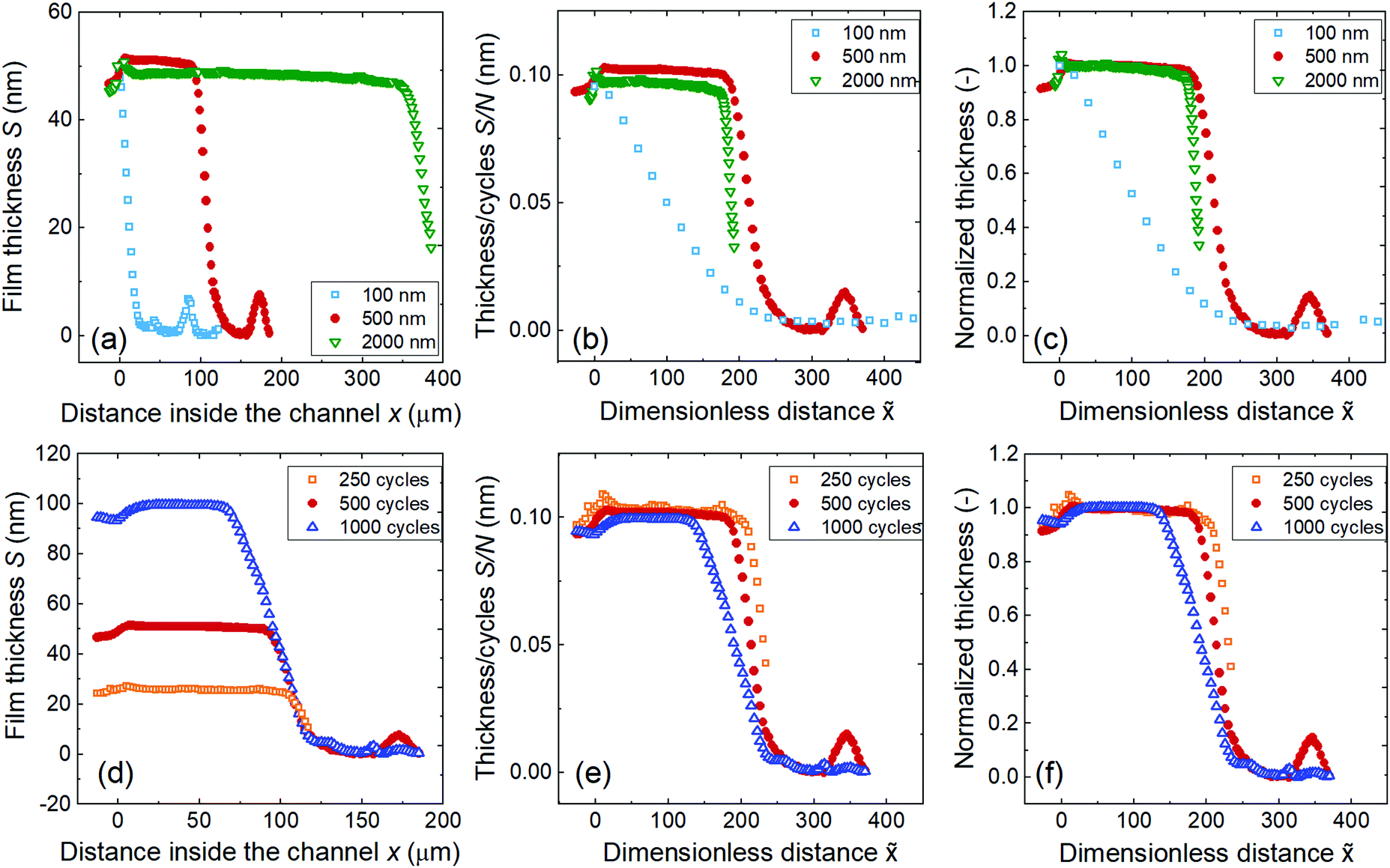 | ||
| Fig. 9 Saturation profile of ALD Al2O3 coated in rectangular LHAR channels at 300 °C. Top row, varying channel height H and constant number of cycles N of 500: (a) as-measured saturation profile, (b) scaled saturation profile, and (c) Type 1 normalized saturation profile. Sample 7, 8, and 9 (Table 1 Series C). Bottom row, varying number of cycles N and constant channel height H of 500 nm: (d) as-measured saturation profile, (e) scaled saturation profile, and (f) Type 1 normalized saturation profile. Sample 8, 10 and 11 (Table 1 Series D). | ||
Fig. 9 (panels d–f) shows the effect of the number of ALD cycles on the Al2O3 ALD saturation profile (Table 1, Series D) for a channel height of 500 nm. The leading edges of the adsorption fronts overlapped; however, film penetration, measured as PD50%, appeared to decrease as the number of cycles increased. The reason for decreasing PD50% is because the ALD process experienced a higher AR as the film filled the channel more (ca. 10%, 20%, and 40% of the channel filled for 250, 500, and 1000 ALD cycles, respectively), thereby restricting film propagation. The slope of the adsorption front became less steep with a higher number of cycles. The effect of the number of cycles on the film thickness outside and inside the channels (Region I and IIb) is reported in Table 1: a linear increase was found in both cases as shown in Fig. S9 (ESI†). SEM-EDS line scans of Al (Fig. S8, ESI†) in samples with a different number of ALD cycles roughly infer a linear relationship between the number of cycles and measured X-ray intensities, in line with the reflectometer measurement results.
The effects of increasing the channel height and number of ALD cycles were simulated with the Ylilammi et al.33 diffusion–reaction model and compared with the experimental saturation profiles. Fig. 10 shows the simulated saturation profiles with various channel heights (panels a–c) and with the number of ALD cycles (panels d–f). For different channel height samples, the scaled saturation profile (Fig. 10b) seemed to approach a process specific “fingerprint” saturation profile when film filling was 20% or less of the channel height. The leading edges of the scaled saturation profiles overlapped, and PD50% decreased when the number of ALD cycles increased. The trends in the simulated results closely resembled the experimental saturation profiles.
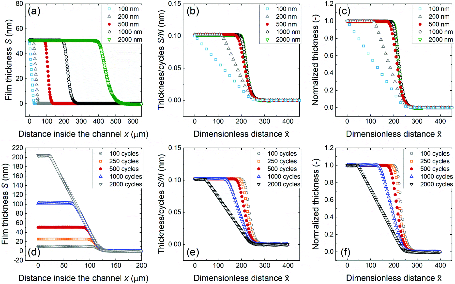 | ||
| Fig. 10 Simulated saturation profiles of ALD Al2O3 in microscopic rectangular LHAR channels, created with a MATLAB re-implementation of the Ylilammi et al.33 diffusion–reaction model. Top row, varying channel height H and constant number of cycles N of 500: (a) as-measured saturation profile, (b) scaled saturation profile, and (c) Type 1 normalized saturation profile. Bottom row, varying number of cycles N and constant channel height H of 500 nm: (d) as-measured, (e) scaled, and (f) normalized saturation profiles of Type 1. Parameter values: T = 300 °C, tP = 0.10 s, pA0 = 65 Pa (A = TMA), pB = 300 Pa (B = N2), MA = 0.075 kg mol−1, MB = 0.028 kg mol−1, dA = 591 pm,33dB = 374 pm, bfilm = 2, bTMA = 1, gpcsat = 0.098 nm, ρ = 3100 kg m−3,51q = 3.6 nm−2, K = 1000.0 Pa−1, cTMA = 0.012, and Pd = 0.043 1 s−1. | ||
E. Characteristics of the TMA–water ALD process
Fig. 11a shows the effect of TMA pulse time on the Al2O3 ALD saturation profile (Series E in Table 1). The TMA dose increased with TMA pulse time, although this increase was not necessarily linear (dose = partial pressure × time; partial pressure is not strictly constant). The penetration depth increased with increasing TMA pulse time, showing a dependency on the precursor dose. For a TMA pulse time of 0.4 s, the adsorption front was notably broadened compared to pulse times of 0.1 and 0.2 s, while GPC remained similar. It seems likely that the TMA dose no longer limited the film growth, and the saturation profile was defined by the water dose. A similar shape change in the ALD saturation profile determining factor was observed recently by Arts et al.36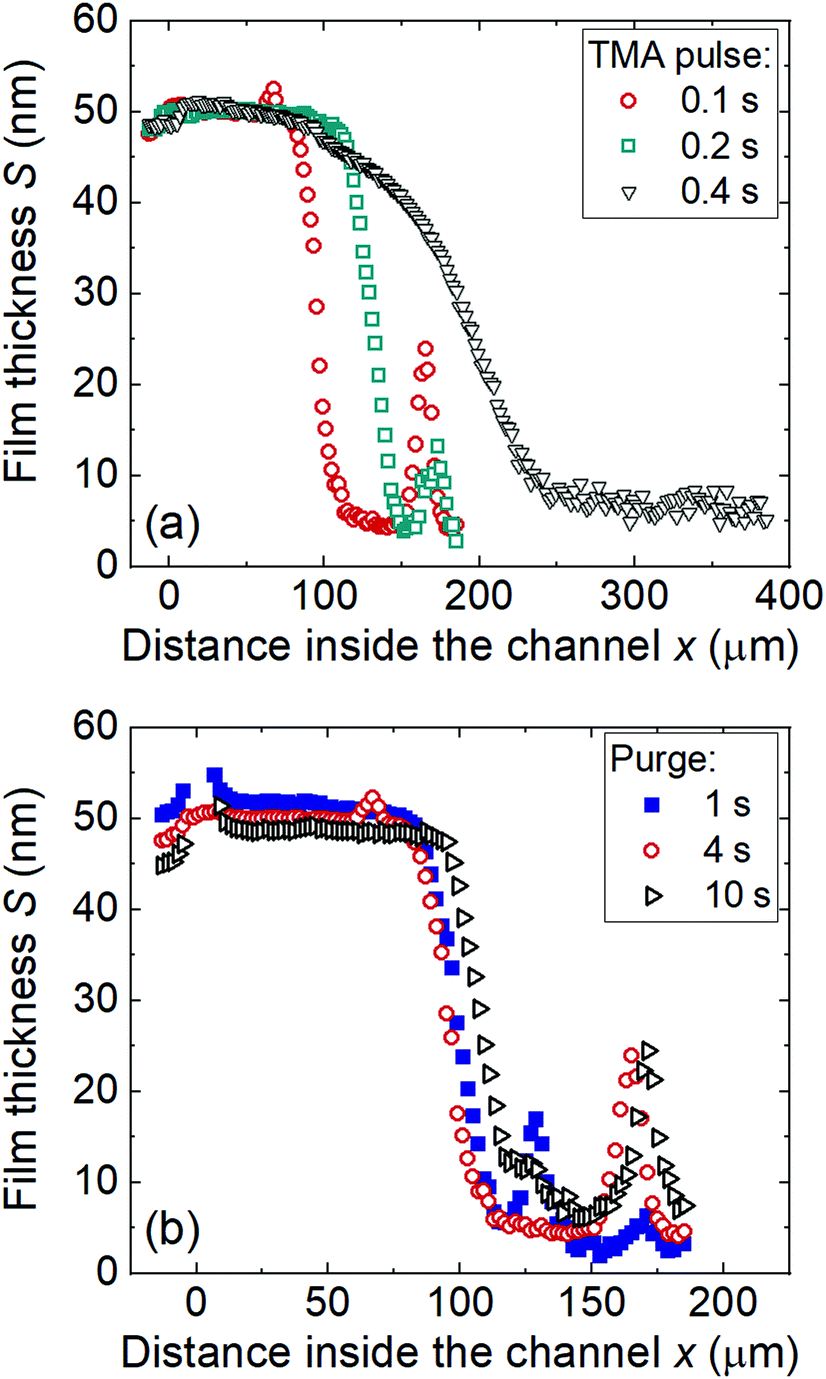 | ||
| Fig. 11 The thicknesses of the Al2O3 ALD film grown at 300 °C using (a) different TMA pulse times (sample 12, 13, and 14 in Table 1 Series E) and (b) purge times in the LHAR channel with a design channel height of 500 nm (sample 12, 15, and 16 in Table 1 Series F). Note that the horizontal scale differs in (a) vs. (b). | ||
Fig. 11b shows the effect of purge time on the TMA–water saturation profile. Purge times after the TMA and water reactions were extended by the same amount. In all cases, the as-measured saturation profile presents a constant thickness region before a sharp decrease. The GPC slightly decreased when the purge time increased from 1 to 10 s, while PD50% slightly increased (Series F in Table 1). The decrease was slightly but noticeably larger in Region I (located outside the LHAR channel) than in Region II (located inside the channel).
E. Discussion
A. Uncertainty sources in experimental saturation profile measurement
Uncertainty in the measured saturation profile stems primarily from (a) uncertainty over the characteristics of LHAR channels caused by their fabrication, (b) uncertainty related to the saturation profile measurement, and (c) uncertainty over the ALD process parameter values used. In the next paragraphs, we discuss each uncertainty source separately.Related to (i), we estimate that during fabrication, tolerance for the oxide thickness that defines the channel height was ±10, 20, and 30 nm for 100, 500, and 2000 nm design channel heights, respectively. These numbers were obtained from the thickness of silicon oxide measured during LHAR channel fabrication, as reported in Table S5 (ESI†). Here, the relative uncertainty of the channel height is larger, the smaller the design height. There may also be other, as yet unidentified factors that result in deviation of the real channel height from the design height; measurement of the real channel height is thus advisable. According to our estimation (Fig. S10, ESI†), for a channel height of 500 nm, a 1% error in the channel height causes roughly a 1.5% error in the penetration depth. Related to (ii), according to the analysis presented in Section 3.2 of the ESI,† for a 500 nm channel the effect of pillars on the penetration depth will be less than 1% (Fig. S11 and S12, ESI†) for a typical pillar diameter of 4 μm and an interdistance of 49 μm in a triangular symmetry. Related to (iii), according to the AFM measurements, in the LHAR channel with 500 nm channel heights, the membrane bent to a displacement of ca. 25 nm (Fig. S13a, ESI†). Bending was measured also for the 2000 nm design, and it was about the same as for the 500 nm design. The 100 nm design channel height bent ca. 40 nm (Fig. S13b, ESI†). Related to (iv–v), the nanostep decreased the channel height, and the roughness thereafter increased the surface area compared to the flat surface assumed in design and modelling. Consequently, the apparent GPC increased (measured vertically), as the surface bound more molecules per distance measurement unit than a completely flat surface would bind. Also, PD50% should be slightly smaller and the slope at PD50% should be somewhat steeper than on a flat surface.
Concerning the fabrication-related uncertainty of the LHAR channels reported in this work, those with a design channel height of 500 nm and pillar layout v1b succeeded best in reproducing the design target and are expected to provide the most reliable saturation profile measurements.
The reproducibility of the saturation profile measurement can be visualized by comparing data from fully independent measurements of the TMA–water saturation profile at 300 °C, as done in Fig. 8b. While there is variation in the film thickness in the flat region and in the penetration depth, the overall saturation profile and the slope at PD50% seem similar in all cases. Based on the data reported in Table 1 for samples 2, 4, 8, and 12, the standard deviation of PD50% and the slope at PD50% were 19.4 μm and 0.0003 nm, respectively. The standard deviation of the initial film thickness in Region IIb was 2.8 nm.
B. Occasional spikes in the saturation profile
Spikes preceding the leading edge were occasionally observed in the saturation profiles (Fig. 3). Schwille et al.41 observed spikes in the saturation profile of TMA–water process measured with their MEMS-type conformality test structures by ellipsometry. They proposed that a CVD-related phenomenon might have contributed to the spikes.41 Interestingly, in our case, spikes were observed in the optical reflectometer measurement but not in SEM-EDS (Fig. 5).Detailed inspection revealed that the spikes appeared at locations where the measurement spot was close to pillar remnants, see Fig. S16 (ESI†). More spikes were observed in repeated reflectometer line scan of a sample having the pillar layout design of v1a, which has a smaller pillar interdistance compared to v1b, see Fig. S17 (ESI†). To create reflectometer-based saturation profiles without pillar remnant influence and without spikes, it would be interesting to investigate the TMA–water process on LHAR channels with a less dense pillar network. Making such experiments is out of the scope of this work, however.
C. Insight into the characteristics of the TMA–water ALD process
Our work revealed, in accordance with Arts et al.,36 that TMA-limited and water-limited growth has different characteristic shape of the saturation profile at 300 °C (Fig. 11a).The effect of purge time on the saturation profile of TMA–water ALD process was further investigated. Our results showed an inverse dependency between the value of GPC and the purge length (Fig. 11b and Fig. S14, ESI†). We believe that during the longer purge, reversibly adsorbed water molecules could have desorbed, causing a decrease in the concentration of surface OH groups. Consequently, the amount of TMA adsorbed decreased as the amount of TMA adsorbed depends on the concentration of surface OH groups.13,50 Although the role of the partly reversible water reaction has not been discussed in detail in the ALD literature, our findings are in line with some earlier reports. Ylivaara et al.51 showed that GPC decreased as purge time increased (from 1 s to 4 s). Matero et al.59 reported a higher GPC of the TMA–water ALD process for higher water partial pressure. Gakis et al.56 assumed reversible reaction of water. Sønsteby et al.26 noted that a long purge time can alter GPC due to dehydration on the surface.
In our work, GPCI outside the channel decreased faster than GPCIIb inside the channel opening when the purge time increased (Fig. S14, ESI†). Likely this can be explained by re-adsorption of the desorbed water on the channel surface, leading to slower decrease in GPCIIb as a function of purge time compared to a planar surface. This conclusion is in line with the analysis by Abelson and Girolami2 for desorption during CVD from a HAR feature.
The decrease in binding capacity of the surface towards TMA enabled the reactant molecules to penetrate deeper into the channel before reacting, resulting in an increased penetration depth (Fig. 11b). Increased penetration depth (in PillarHall-1) with decreased GPC has been observed in earlier works by Mattinen et al.47 for iridium ALD and by Puurunen and Gao46 for Al2O3 ALD at different temperatures.
D. Sticking coefficients from saturation profile measurements
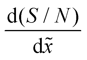
The method developed by Arts et al.36 allows one to calculate the lumped sticking coefficient of reactants from Type 1 normalized saturation profile, provided that the growth is in the Knudsen flow regime. The calculation of lumped sticking coefficient is made with eqn (3) of Arts et al.:36 . To be in the Knudsen flow regime, the molecule's mean free path λ should be significantly larger than the characteristic size of the LHAR structure h. In other words, Knudsen number Kn = λ/h ≫ 1.
To inform whether the Arts et al.36 method can be applied in this work, the mean free path λ was calculated. At 300 °C under the process conditions used in this work, the mean free path [calculated with eqn (3) ref. 1] for TMA and water is 40 and 100 μm, respectively. The characteristic size is interpreted as the hydraulic diameter of the channel h, so that h = 2/(1/H + 1/W). For a 500 nm channel, the hydraulic diameter is thus 1.0 μm, and the Knudsen number is 40 and 100 for TMA and water, respectively. The Arts et al.36 method should thus be valid in our case.
The lumped sticking coefficient calculated in this work from the slope values of Type 1 normalized saturation profile are reported in Table 2. For TMA on Al2O3, the sticking coefficient was calculated from several samples and then averaged; for water, one sample was used. The result is compared with earlier studies in Table 2.36,54,60 Our extracted value of cTMA, 4 × 10⁻³, agrees with the literature values and is in between those reported by Arts et al.36 and Ylilammi et al.33 The extracted value of cH2O of 3 × 10⁻⁴ is also in line with the previously reported values.36,60
| Temperature (°C) | LHAR type | LHAR H (μm) | Max. AR | Number of cycles | Reactor | c TMA | c H2O | Ref. |
|---|---|---|---|---|---|---|---|---|
| a The order of magnitude estimated. The structure had a microscopic cavity with its height of 5 μm, lateral length of 2000 μm, and a single access hole with its diameter range of 4 to 100 μm. b Number of ALD cycles is not reported in the literature. c Although ALD alumina was not coated on a LHAR feature but planar Si(100) wafer, the sticking coefficients obtained are included for reference. d The order of magnitude of lumped sticking coefficients were reported. cH2O of 1 × 10⁻⁴ and 1 × 10⁻⁶ at 300 °C and 100 °C, respectively, and cTMA of 2 × 10⁻³ (temperature-independent) were reported in the follow-up work Vandalon et al. (2017).54 e The alumina film density used by Ylilammi et al.33 was 4000 kg m−3 (not reported in the original publication33), which is higher than in our study (3100 kg m−3). f Calculated for sample 2, 4, 8, and 12 by using Arts et al.36 method, and the results were averaged. g Calculated for sample 14 by using Arts et al.36 method. | ||||||||
| 200 | Macroscopic rectangular | 100 | 200:1 |
150 | Home-built | 0.1 | — | Dendooven et al. (2009)31 |
| 200 | Microscopic centrosymmetric | 4.5 | ∼100:1a |
—b | Single wafer cross-flow hot wall reactor | 2 × 10⁻² | — | Schwille et al. (2016)41 |
| 100–300 | —c | — | —c | —b | Home-built | 10−3d |
10−4d |
Vandalon et al. (2016)60 |
| 300 | Microscopic rectangular PillarHall-3 | 0.50 | 2000:1 |
500 | Picosun R-150 | 5.72 × 10⁻³e |
— | Ylilammi et al. (2018)33 |
| 275 | Microscopic rectangular PillarHall-3 | 0.50 | 10000:1 |
400 | Oxford instruments OpAL reactor | (0.5–2) × 10−3 | (0.8–2) × 10−4 | Arts et al. (2019)36 |
| 300 | Microscopic rectangular PillarHall-3 | 0.50 | 10000:1 |
500 | Picosun R-150 | 4 × 10⁻³f |
3 × 10⁻⁴g |
This work |
F. Conclusions
This work created a benchmark for saturation profile based conformality analysis of ALD processes in rectangular microscopic LHAR channels. As a test vehicle, the archetypical TMA–water process at the typical ALD temperature of 300 °C was used. The effect of variations in LHAR structure prototype's actual dimensions, effect of support pillars on growth, the ALD process reproducibility, and the thickness measurement uncertainty were discussed. Classifications and terminology related to saturation profile based conformality analysis were developed. The classifications and terminology should be applicable to other LHAR-based saturation profile based conformality studies of ALD and potentially, at least partly, also CVD and ALE studies.The as-measured saturation profiles of thickness vs. distance differed for the TMA–water process, depending on the number of cycles (250–1000) and the LHAR channel height employed (design height 100, 500, 2000 nm). The saturation profiles approached the same values, when they were scaled with the number of ALD cycles and the LHAR channel height. We propose the scaled saturation profile as an informative measure of an ALD process, which at favorable conditions can become a characteristic fingerprint of an ALD process. Favorable conditions refer at least to that gas-phase transport should be in the Knudsen diffusion regime and the LHAR channel should remain sufficiently open (channel filling preferably less than 10%).
The saturation profile of ALD Al2O3 showed a near-ideal shape expected for an ALD process based on repeated self-terminating gas–solid reactions, namely a constant thickness before a steep decrease to zero. The measured saturation profile was not influenced by different lateral lengths of the LHAR channel (100 μm to 5 mm). Depending on the magnitude of ALD reactant exposures, different limiting regimes can govern the ALD growth in LHAR channels. With increasing TMA dose, the growth transformed from TMA-dose-limited to water-dose-limited. Contrasting the ideality assumption of fully irreversible ALD reactions, we observed changes in the saturation profile with increasing purge times. This observation can likely be related to a reversible component in the water reaction with the TMA-modified surface in an ALD cycle. Lumped sticking coefficients calculated from the slope of the saturation profile, agreed with previously reported values.
Funding sources
Funding for PillarHall-3 LHAR prototype fabrication at VTT was provided by the Academy of Finland via the Finnish Centre of Excellence on Atomic Layer Deposition and via Tekes (currently: Business Finland) via the PillarHall TUTL project (1125/31/2016). The work at Aalto University was supported by Puurunen's starting grant and by the Academy of Finland (COOLCAT consortium, decision no. 329978 and ALDI consortium, decision no. 331082).Symbols and abbreviations
In this work, we have largely followed the notation of Ylilammi et al. 2018.33 Additionally, we have taken influence from Arts et al.36| a | Distance between pillars (m) |
| A | Surface area (m2) |
| c TMA | Lumped sticking coefficient of TMA |
| c H2O | Lumped sticking coefficient of water |
| b | Number of metal atoms in a molecule |
| d | Pillar diameter (μm) |
| d A | Molecular diameter of Reactant A (pm) |
| d B | Molecular diameter of carrier gas B (pm) |
| D | Apparent diffusion coefficient (m2 s−1) |
| D 0 | Diffusion coefficient without pillars (m2 s−1) |
| F | Flux of material in direction x (mol m−2 s−1) |
| GPC | Growth per cycle (m) |
| gpc sat | Saturation growth in cycle (nm) |
| H | Channel height (nm) |
| h | Hydraulic diameter (μm) |
| K | Adsorption equilibrium constant (1 Pa−1) |
| K n | Knudsen number (−) |
| L | Lateral length of the channel (μm) |
| l | Distance between rows of pillars (μm) |
| M B | Molar mass of carrier gas B (kg mol−1) |
| M A | Molar mass of reactant A (kg mol−1) |
| N | Number of cycles |
| p A0 | Input partial pressure of Reactant A (Pa) |
| p B | Partial pressure of carrier gas B (Pa) |
| PD50% | Penetration depth at 50% of film thickness (μm) |
| P d | Desorption probability in unit time (1 s−1) |
| Q | Collision rate at unit pressure (m−2 s−1 Pa−1) |
| q | Adsorption density of reactant A at saturation (1 m−2) |
| R | Diffusion resistance of a rectangular channel (s m−3) |
| R row | Diffusion resistance of one row of pillars (s m−3) |
| S I | Film thickness outside the channel (m) |
| S II | Film thickness inside the channel (m) |
| t P | Pulse length (s) |
| W | Opening width of the channel (m) |
| x | Distance from channel opening (m) |
| x 50% | 50% thickness penetration depth (μm) |
|
| dimensionless distance (−) |
| λ TMA | Mean free path of TMA (μm) |
| ρ | Film density (kg m−3) |
| θ | Surface coverage (0 ≤ θ ≤ 1) |
| ξ | Normalized distance (−) |
Conflicts of interest
R. L. P developed the concept of the microscopic LHAR conformality test and is the inventor of a related patent application. VTT has made PillarHall™ test structure prototypes available for purchase. M. U. is responsible for PillarHall™ test structure sales and commercialization activities at VTT and is the founder of Chipmetrics Oy.Acknowledgements
R. L. P. acknowledges the expert help of colleagues at VTT Micronova, without whom the PillarHall-3 fabrication would not have succeeded: MEMS processing learnings collection compiled by James Dekker; general advice from Jaakko Saarilahti; valuable learnings from earlier PillarHall fabrication runs from Feng Gao; lithography mask drawing by Harri Pohjonen; supervising after R. L. P. of the PillarHall-3 fabrication by Mari Laamanen; and skillful clean room fabrication from Meeri Partanen and Tuomo Honkaharju. J. Ruud van Ommen is thanked for his comments on the manuscript. This work made use of Aalto University RawMatters and OtaNano infrastructures. The PillarHall-3 structures were first introduced, the influence of the pillars on film growth was analyzed and saturation profile related terminology development was initiated at the EUROCVD21-Baltic ALD 15 conference, Linköping, Sweden, June 11–14, 2017; at this conference, Angel Yanguas-Gil used the term “saturation profile”. The measurement spot size effect was first discussed at the AVS 17th International Conference on Atomic Layer Deposition (ALD 2017), Denver, Colorado, July 15–18, 2017. The saturation profile data and simulations of this work were introduced at the EuroCVD 22-Baltic ALD 16 Conference, Luxembourg, June 24–28, 2019. The uncertainty components were introduced at Nanoscale 2019, Braunschweig, Germany, October 15–16, 2019. The saturation profile classification was proposed at the 66th AVS International Symposium and Exhibition, Columbus, Ohio, October 20–25, 2019. Our experimental saturation profile data is planned to be uploaded to Zenodo for open access viahttps://zenodo.org/communities/ald-saturation-profile-open-data/.References
- V. Cremers, R. L. Puurunen and J. Dendooven, Appl. Phys. Rev., 2019, 6, 021302 Search PubMed.
- J. R. Abelson and G. S. Girolami, J. Vac. Sci. Technol., A, 2020, 38, 030802 CrossRef CAS.
- A. van Asten, F. Roozeboom, R. Knaapen, P. Poodt and A. Illiberi, J. Vac. Sci. Technol., A, 2011, 30, 01A142 Search PubMed.
- H. G. Kim and H. B. R. Lee, Chem. Mater., 2017, 29, 3809–3826 CrossRef CAS.
- P. Munnik, P. E. De Jongh and K. P. De Jong, Chem. Rev., 2015, 115, 6687–6718 CrossRef CAS.
- B. J. O’Neill, D. H. K. Jackson, J. Lee, C. Canlas, P. C. Stair, C. L. Marshall, J. W. Elam, T. F. Kuech, J. A. Dumesic and G. W. Huber, ACS Catal., 2015, 5, 1804–1825 CrossRef.
- T. Onn, R. Küngas, P. Fornasiero, K. Huang and R. Gorte, Inorganics, 2018, 6, 34 CrossRef.
- P. Voigt, E. Haimi, J. Lahtinen, Y. W. Cheah, E. Mäkelä, T. Viinikainen and R. L. Puurunen, Top. Catal., 2019, 62, 611–620 CrossRef CAS.
- O. Graniel, M. Weber, S. Balme, P. Miele and M. Bechelany, Biosens. Bioelectron., 2018, 122, 147–159 CrossRef CAS.
- P. Poodt, A. Lankhorst, F. Roozeboom, K. Spee, D. Maas and A. Vermeer, Adv. Mater., 2010, 22, 3564–3567 CrossRef CAS.
- A. S. Asundi, J. A. Raiford and S. F. Bent, ACS Energy Lett., 2019, 4, 908–925 CrossRef CAS.
- M. Ritala and M. Leskelä, in Handbook of Thin Films Materials: Deposition and Processing of Thin Films, ed. H. S. Nalwa, Academic Press, 2002, pp. 103–159 Search PubMed.
- R. L. Puurunen, J. Appl. Phys., 2005, 97, 121301 CrossRef.
- M. G. Steven, Chem. Rev., 2010, 110, 111–131 CrossRef.
- H. Van Bui, F. Grillo and J. R. Van Ommen, Chem. Commun., 2017, 53, 45–71 RSC.
- FIN 52359, U.S. patent 4 058 430 (25 November 1975), 1974.
- R. L. Puurunen, Chem. Vap. Deposition, 2014, 20, 332–344 CrossRef CAS.
- G. N. Parsons, J. W. Elam, S. M. George, S. Haukka, H. Jeon, W. M. M. (Erwin) Kessels, M. Leskelä, P. Poodt, M. Ritala and S. M. Rossnagel, J. Vac. Sci. Technol., A, 2013, 31, 050818 CrossRef.
- G. N. Parsons, J. W. Elam, S. M. George, S. Haukka, H. Jeon, W. M. M. (Erwin) Kessels, M. Leskelä, P. Poodt, M. Ritala and S. M. Rossnagel, J. Vac. Sci. Technol., A, 2020, 38, 037001 CrossRef CAS.
- V. B. Aleskovskii and S. I. Koltsov, Abstract of Scientific and Technical Conference, Goskhimizdat, Leningrad 1965, 67 (in Russian).
- A. A. Malygin, V. E. Drozd, A. A. Malkov and V. M. Smirnov, Chem. Vap. Deposition, 2015, 21, 216–240 CrossRef CAS.
- E. Ahvenniemi, A. R. Akbashev, S. Ali, M. Bechelany, M. Berdova, S. Boyadjiev, D. C. Cameron, R. Chen, M. Chubarov, V. Cremers, A. Devi, V. Drozd, L. Elnikova, G. Gottardi, K. Grigoras, D. M. Hausmann, C. S. Hwang, S.-H. Jen, T. Kallio, J. Kanervo, I. Khmelnitskiy, D. H. Kim, L. Klibanov, Y. Koshtyal, A. O. I. Krause, J. Kuhs, I. Kärkkänen, M.-L. Kääriäinen, T. Kääriäinen, L. Lamagna, A. A. Łapicki, M. Leskelä, H. Lipsanen, J. Lyytinen, A. Malkov, A. Malygin, A. Mennad, C. Militzer, J. Molarius, M. Norek, Ç. Özgit-Akgün, M. Panov, H. Pedersen, F. Piallat, G. Popov, R. L. Puurunen, G. Rampelberg, R. H. A. Ras, E. Rauwel, F. Roozeboom, T. Sajavaara, H. Salami, H. Savin, N. Schneider, T. E. Seidel, J. Sundqvist, D. B. Suyatin, T. Törndahl, J. R. van Ommen, C. Wiemer, O. M. E. Ylivaara and O. Yurkevich, J. Vac. Sci. Technol., A, 2017, 35, 010801 CrossRef.
- D. Cord, Finnish Physicist Tuomo Suntola Wins Millennium Technology Prize, https://finland.fi/business-innovation/finnish-physicist-tuomo-suntola-wins-millennium-technology-prize/, accessed 12 December 2019.
- J. W. Elam, D. Routkevitch, P. P. Mardilovich and M. G. Steven, Chem. Mater., 2003, 15, 3507–3517 CrossRef CAS.
- N. E. Richey, C. De Paula and S. F. Bent, J. Chem. Phys., 2020, 152, 040902 CrossRef CAS.
- H. H. Sønsteby, A. Yanguas-gil, J. W. Elam and J. W. Elam, J. Vac. Sci. Technol., A, 2020, 38, 020804 CrossRef.
- A. Yanguas-Gil, Growth and Transport in Nanostructured Materials: Reactive Transport in PVD, CVD, and ALD, Springer, 2016 Search PubMed.
- H. C. M. Knoops, E. Langereis, M. C. M. van de Sanden and W. M. M. Kessels, J. Electrochem. Soc., 2010, 157, G241–G249 CrossRef CAS.
- R. G. Gordon, D. Hausmann, E. Kim and J. Shepard, Chem. Vap. Deposition, 2003, 9, 73–78 CrossRef CAS.
- M. C. Schwille, T. Schössler, J. Barth, M. Knaut, F. Schön, A. Höchst, M. Oettel and J. W. Bartha, J. Vac. Sci. Technol., A, 2016, 35, 01B118 CrossRef.
- J. Dendooven, D. Deduytsche, J. Musschoot, R. L. Vanmeirhaeghe and C. Detavernier, J. Electrochem. Soc., 2009, 156, P63–P67 CrossRef CAS.
- A. Yanguas-Gil and J. W. Elam, Chem. Vap. Deposition, 2012, 18, 46–52 CrossRef CAS.
- M. Ylilammi, O. M. E. Ylivaara and R. L. Puurunen, J. Appl. Phys., 2018, 123, 205301 CrossRef.
- P. Poodt, A. Mameli, J. Schulpen, W. M. M. (Erwin) Kessels and F. Roozeboom, J. Vac. Sci. Technol., A, 2017, 35, 021502 CrossRef.
- M. Rose and J. W. Bartha, Appl. Surf. Sci., 2009, 255, 6620–6623 CrossRef CAS.
- K. Arts, V. Vandalon, R. L. Puurunen, M. Utriainen, F. Gao, W. M. M. Kessels and H. C. M. Knoops, J. Vac. Sci. Technol., A, 2019, 37, 030908 CrossRef.
- K. E. Elers, T. Blomberg, M. Peussa, B. Aitchison, S. Haukka and S. Marcus, Chem. Vap. Deposition, 2006, 12, 13–24 CrossRef CAS.
- M. Ladanov, P. Algarin-Amaris, G. Matthews, M. Ram, S. Thomas, A. Kumar and J. Wang, Nanotechnology, 2013, 24, 375301 CrossRef CAS.
- J. Dendooven, D. Deduytsche, J. Musschoot, R. L. Vanmeirhaeghe and C. Detavernier, J. Electrochem. Soc., 2010, 157, G111–G116 CrossRef CAS.
- F. Gao, S. Arpiainen and R. L. Puurunen, J. Vac. Sci. Technol., A, 2015, 33, 010601 CrossRef.
- M. C. Schwille, T. Schössler, F. Schön, M. Oettel and J. W. Bartha, J. Vac. Sci. Technol., A, 2017, 35, 01B119 CrossRef.
- A. M. Kia, N. Haufe, S. Esmaeili, C. Mart, M. Utriainen, R. L. Puurunen and W. Weinreich, Nanomaterials, 2019, 9, 1035 CrossRef CAS.
- L. Souqui, H. Högberg and H. Pedersen, Chem. Mater., 2019, 31, 5408–5412 CrossRef CAS.
- K. Arts, M. Utriainen, R. L. Puurunen, W. M. M. E. Kessels and H. C. M. Knoops, J. Phys. Chem. C, 2019, 1–11 Search PubMed.
- V. Miikkulainen, M. Leskelä, M. Ritala and R. L. Puurunen, J. Appl. Phys., 2013, 113, 021301 CrossRef.
- R. L. Puurunen and F. Gao, 14th Int. Balt. Conf. At. Layer Depos. (BALD), St. Petersbg., 2016, 20–24.
- M. Mattinen, J. Hämäläinen, F. Gao, P. Jalkanen, K. Mizohata, J. Räisänen, R. L. Puurunen, M. Ritala and M. Leskelä, Langmuir, 2016, 32, 10559–10569 CrossRef CAS.
- K. Arts, J. H. Deijkers, T. Faraz, R. L. Puurunen, W. M. M. E. Kessels and H. C. M. Knoops, Appl. Phys. Lett., 2020, 117, 031602 CrossRef CAS.
- M. J. Young, A. Yanguas-gil, S. Letourneau, M. Coile, D. Mandia, M. Bedford, B. Aoun, A. S. Cavanagh, S. M. George and J. W. Elam, ACS Appl. Mater. Interfaces, 2020, 1–22 Search PubMed.
- R. L. Puurunen, Appl. Surf. Sci., 2005, 245, 6–10 CrossRef CAS.
- O. M. E. Ylivaara, X. Liu, L. Kilpi, J. Lyytinen, D. Schneider, M. Laitinen, J. Julin, S. Ali, S. Sintonen, M. Berdova, E. Haimi, T. Sajavaara, H. Ronkainen, H. Lipsanen, J. Koskinen, S.-P. Hannula and R. L. Puurunen, Thin Solid Films, 2014, 552, 124–135 CrossRef CAS.
- M. Shirazi and S. D. Elliott, Nanoscale, 2015, 7, 6311–6318 RSC.
- T. Weckman and K. Laasonen, Phys. Chem. Chem. Phys., 2015, 17, 17322–17334 RSC.
- V. Vandalon and W. M. M. (Erwin) Kessels, J. Vac. Sci. Technol., A, 2017, 35, 05C313 CrossRef.
- J. M. Lownsbury, J. A. Gladden, C. T. Campbell, I. S. Kim and A. B. F. Martinson, Chem. Mater., 2017, 29, 8566–8577 CrossRef CAS.
- G. P. Gakis, H. Vergnes, E. Scheid, C. Vahlas, A. G. Boudouvis and B. Caussat, Chem. Eng. Sci., 2019, 195, 399–412 CrossRef CAS.
- B. A. Sperling, B. Kalanyan and J. E. Maslar, J. Phys. Chem. C, 2020, 124, 3410–3420 CrossRef CAS.
- A. Yanguas-Gil and J. W. Elam, J. Vac. Sci. Technol., A, 2012, 30, 01A159 CrossRef.
- R. Matero, A. Rahtu, M. Ritala, M. Leskelä and T. Sajavaara, Thin Solid Films, 2000, 368, 1–7 CrossRef CAS.
- V. Vandalon and W. M. M. Kessels, Appl. Phys. Lett., 2016, 108, 011607 CrossRef.
Footnotes |
| † Electronic supplementary information (ESI) available: Extended information on experimental, results, and discussion sections. See DOI: 10.1039/d0cp03358h |
| ‡ These authors contributed equally to this work. |
| This journal is © the Owner Societies 2020 |