Indium electrodeposition from indium(III) methanesulfonate in DMSO†
Received
18th June 2020
, Accepted 11th September 2020
First published on 22nd October 2020
Abstract
The electrochemical behavior and electrodeposition of indium was investigated at 26 °C and 160 °C from a solution composed of indium(III) methanesulfonate and dimethylsulfoxide (DMSO). Indium(III) methanesulfonate was synthesized from indium(III) oxide and methanesulfonic acid (MSA). Cyclic voltammetry, quartz crystal microbalance measurements and rotating ring disk electrode experiments indicated that reduction of indium(III) to both indium(I) and indium(0) occurs. Yet, reduction to metallic indium was found to be the predominant process. Deposited indium could be stripped to indium(I). This unstable species disproportionated to indium(III) and indium(0), leading to the formation of micron-sized metallic indium particles in the electrolyte. At 26 °C, indium deposited on glassy carbon as smooth, flat films whereas at 160 °C, it deposits as droplets.
Introduction
Indium is a metal which has found many technological applications in the last three decades. Especially in the electronics industry, several semiconductors incorporate indium as a principal component. These include indium tin oxide (ITO), indium phosphide (InP) and copper indium (gallium) selenide (CI(G)S), used in devices such as flat panel displays, light-emitting diodes, solar cells and lasers.1–3 Due to the growing demand for indium by the electronics industry, combined with the limited supply of indium from primary sources, interest is arising to develop efficient methods for refining indium to high-grade semi-conductor quality, and to recycle indium from end-of-life products as a secondary supply route.4,5
Electrodeposition has been proven to be effective for refining of metals, and is often implemented in industry. This method is particularly favorable because of its simplicity and flexibility, and its cost-effectiveness in terms of equipment and required chemicals.6
Electrodeposition of indium from aqueous solutions has been extensively studied and is well understood.7–9 The standard reduction potential of the In3+/In couple is −0.34 V.10 Due to this negative standard reduction potential, the electrodeposition of indium from aqueous electrolytes competes with the hydrogen evolution reaction (HER), i.e., the reduction of water, or protons.7,8 Non-aqueous electrolytes have been explored to avoid concomitant hydrogen evolution, and to be operative at elevated temperatures. The latter is particularly interesting since the melting point of indium is as low as 156.6 °C. Non-aqueous solutions that exhibit high thermal stability and a high boiling point can be exploited to electrodeposit indium in molten form. This enables the development of a continuous system in which molten indium can be electrodeposited, collected and continuously removed at the bottom of the electrochemical reactor.11
Several non-aqueous, thermally stable electrolytes have been reported for indium electrodeposition. Once such example are high temperature molten salts.12,13 The HER does not occur in these systems due to the absence of water. Yet, molten salt electrolytes require a substantial amount of thermal energy, which renders them less desirable for use in large-scale industrial operations. Ionic liquids, deep-eutectic solvents (DES) and several organic electrolytes are more promising alternatives, as they have high (electro)chemical and thermal stabilities, but operate at lower temperatures.11,14–19 They support metal deposition in a broad potential and temperature range. However, ionic liquids and DES often have high viscosities, which hampers ion transport towards the electrode, lowering achievable current densities and thus deposition rates.
In a previous study, we described indium electrodeposition at room temperature and at 160 °C from the organic solvents 1,2-dimethoxyethane and poly(ethylene) glycol, respectively, using a mixture of indium(III) chloride and indium(III) bistriflimide as indium source.19 The latter salt was synthesized by reaction between indium(III) oxide and bistriflimidic acid (Tf2NH). From a recycling perspective, conversion of indium(III) oxide, or indium(III) hydroxide, to a compound that can be electrochemically reduced in solution to pure indium metal is interesting, as the oxide and hydroxide are intermediates formed during the purification of indium from primary and secondary resources.20 In principle, transformation of these intermediates into metallic indium could therefore lower the energetic cost of its production.
In this study, this concept of electrodeposition of indium from non-aqueous electrolytes is further expanded, by studying the electrodeposition of this metal from an electrolyte comprised of indium(III) methanesulfonate and dimethylsulfoxide (DMSO). Similarly to indium(III) bistriflimide, indium(III) methanesulfonate is prepared from indium(III) oxide. However, no indium(III) chloride is added. Therefore, electrodeposition of indium fully originates from chemically converted indium(III) oxide.
Experimental
Chemicals
Indium(III) oxide (99.9%) was purchased from Thermo Fisher (Merelbeke, Belgium). Methanesulfonic acid (MSA, 99.5%) was purchased from Carl Roth (Karlsruhe, Germany). Dimethylsulfoxide (DMSO, anhydrous, 99%) was purchased from Acros Organics (Thermo Fisher Scientific, Geel, Belgium). HCl (Analar Normapur, 37%) was purchased from VWR (Leuven, Belgium), tetrabutylammonium methanesulfonate ([TBA][OMs], 97%), 1-butyl-1-methylpyrrolidinium bis(trifluoromethylsulfonyl)imide ([BMP][Tf2N], 98%) and potassium hexacyanoferrate(III) (K3Fe(CN)6) were purchased from Sigma-Aldrich (Overijse, Belgium) and acetone (99+%) was purchased from Chem-Lab (Zedelgem, Belgium). All chemicals were used as received, without further purification.
Electrochemical methods and analysis techniques
All electrochemical experiments were performed in an argon-filled glovebox with oxygen and moisture concentrations below 1 ppm, and performed using an Autolab PGSTAT 302N potentiostat, controlled by a computer with NOVA2 software. Measurements were carried out using a three-electrode setup. Disk electrodes made out of platinum or glassy carbon wires embedded in glass and a diameter of 1 mm served as working electrode (WE) for recording cyclic voltammograms (CVs), whereas glassy carbon plates with exposed surface areas of 20 mm2 were used as WE for deposition experiments. For all experiments, the counter electrode (CE) consisted of a coiled platinum wire with a diameter of 1 mm whose area was at least five times larger than that of the WE and the reference electrode (RE) was a ferrocene/ferrocenium electrode, consisting of a glass tube filled with a solution of ferrocene (5 mM) and ferrocenium (5 mM) in 1-butyl-1-methyl-pyrrolidini-um bis(trifluoromethylsulfonyl)imide, [BMP][Tf2N], in which a platinum wire was immersed. Prior to use, platinum wires and platinum-coated silicon wafer pieces were washed with HCl (35%), rinsed with demineralized water and acetone, and air-dried. A ceramic crucible was used as electrochemical cell in which 3 mL of electrolyte was added. Electrochemical measurements were performed at either 26 °C or 160 °C. For rotating ring disk electrode (RRDE) experiments, a ring-disk electrode was used where the disk consisted of platinum and the ring of gold (Gaossunion, RRDE-A3). The diameter of the disk was 5.5 mm, whereas the inner and outer diameter of the ring were 6.5 mm and 7.5 mm, respectively. Electrochemical Quartz Crystal Microbalance (EQCM) measurements were performed using platinum-coated QCM-crystals (1 inch, 5 MHz AT-cut platinum-coated crystals, INFICON) with an electrochemically active surface of 121 mm2. Experiments were executed using an EQCM device (MaxTek) that was connected to the Autolab PGSTAT 302N potentiostat. The morphology of the indium deposits on various substrates was studied using scanning electron microscopy (SEM; Phillips XL-30 FEG). For elemental analysis, energy-dispersive X-ray analysis was used (EDX; Octane elite super silicon drift detector, Ametek EDAX). The X-ray diffraction (XRD) diffractograms were measured using a Seifert XRD 3003 TT. The viscosity of the solutions was determined using a rolling-ball type viscometer (AntonPaar, Lovis 2000 ME) and the density of the solutions was determined using a density meter with an oscillating Utube sensor (AntonPaar, DMA 4500 M). The infrared spectra were recorded at a resolution of 4 cm−1, using an attenuated total reflectance (ATR) technique on a Bruker Vertex 70 FTIR spectrometer, with a Platinum ATR extension. Assignment of the peaks was based on the available literature. FTIR (ATR, νmax/cm−1): 3018, 2921 (CH3), 1275, 1261 (SO3), 1061, 1042 (SO3), 981, 970, 961, 901 (CH3), 783 (C–S stretch), 568 (SO3), 545, 525, 496 (SO3).
Synthesis
Indium(III) methanesulfonate.
Indium(III) methanesulfonate, In(CH3SO3)3, was synthesized by mixing indium(III) oxide (In2O3, molecular mass 0.2776 kg mol−1) and methanesulfonic acid (MSA, CH3SO3H, molecular mass 0.0961 kg mol−1) in a molar ratio of 1![[thin space (1/6-em)]](https://www.rsc.org/images/entities/char_2009.gif) :6 in 50 mL of demineralized water. The solution was vigorously stirred at 900 rpm and heated to a temperature of 90 °C for 48 hours using a reflux setup. A small excess of indium(III) oxide was added to force the reaction to completion, at which the pH of the solution became neutral (pH = 7). Hence, the MSA completely reacted away. Subsequently, the formed indium(III) methanesulfonate was separated from the solution by removal of water by evaporation using a rotary evaporator (<1 mbar, 55 °C), and finally dried on a vacuum line (<0.001 mbar) for 48 hours at 125 °C, resulting in a white powder (3.2 g, yield 95%). The synthesized salt was stored in an argon-filled glovebox.
:6 in 50 mL of demineralized water. The solution was vigorously stirred at 900 rpm and heated to a temperature of 90 °C for 48 hours using a reflux setup. A small excess of indium(III) oxide was added to force the reaction to completion, at which the pH of the solution became neutral (pH = 7). Hence, the MSA completely reacted away. Subsequently, the formed indium(III) methanesulfonate was separated from the solution by removal of water by evaporation using a rotary evaporator (<1 mbar, 55 °C), and finally dried on a vacuum line (<0.001 mbar) for 48 hours at 125 °C, resulting in a white powder (3.2 g, yield 95%). The synthesized salt was stored in an argon-filled glovebox.
Results and discussion
For the preparation of indium(III) methanesulfonate, indium(III) oxide was mixed with methanesulfonic acid (MSA):| | | In2O3 + 6CH3SO3H → 2In(CH3SO3) + 3H2O | (1) |
In contrast to bistriflimidic acid, MSA is relatively inexpensive and biodegradable. It is therefore favorable to convert indium(III) oxide to indium(III) methanesulfonate rather than indium(III) bistriflimide. Synthesis of indium(III) methanesulfonate has not been reported in literature. However, a large number of metal methanesulfonates have already been characterized.21–23 Furthermore, tin(II) methanesulfonate has been synthesized and used as precursor for tin electroplating from a bath composed of MSA and the ionic liquid 1-butyl-1-methyl-pyrrolidinium trifluoromethanesulfonate ([BMP][OTf]).24 The prepared indium(III) methane-sulfonate was dissolved in DMSO. This solvent exhibits considerable electrochemical stability and has a boiling point of 189 °C, enabling the electrodeposition of indium above its melting point.
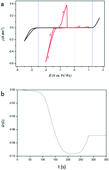
Cyclic voltammograms (CVs) of DMSO with 0.25 mol dm−3 of tetrabutylammonium methanesulfonate, added as inert background salt, (black) and of DMSO with 0.25 mol dm−3 of indium(III) methanesulfonate (red) are shown in Fig. 1a. The measurements were recorded at 26 °C, on a platinum working electrode (WE). The cathodic and anodic breakdown of DMSO occur at −2.52 V vs. Fc+/Fc and +1.30 V vs. Fc+/Fc, respectively, indicating that the electrochemical window of DMSO is 3.52 V wide, which is in good agreement with literature.25 For the indium-containing solution, an onset in reduction current is observed at −1.42 V vs. Fc+/Fc. In standard conditions, the following reduction reactions for indium are known:9
| | | In3+ + 3e− ⇌ In E0 = −0.3382 V | (2) |
| | | In3+ + 2e− ⇌ In+ E0 = −0.443 V | (3) |
| | | In+ + e− ⇌ In E0 = −0.139 V | (4) |
 |
| | Fig. 1 (a) CVs of 0.25 mol dm−3 tetrabutylammonium methanesulfonate in DMSO (black) and of 0.25 mol dm−3 of In(CH3SO3)3 in DMSO (red) on a platinum WE (1 mm diameter) at a scan rate of 10 mV s−1 at 26 °C. (b) Coulombic charge as a function of time, derived from the CV (red) in (a). | |
While indium(I) has been identified in a number of studies, the existence of indium(II) has not been reported.11,16,18,19 Therefore, this species was not considered in our study. Because of the presence of a nucleation loop in the red CV in Fig. 1a, which is a typical feature for metal deposition, the observed reduction process is assumed to be the reduction of indium(III) to indium(0). However, the involvement of indium(I) is not excluded. In the backward scan, an oxidation peak is seen at −1.08 V vs. Fc+/Fc and is likely the stripping of the deposited indium. Interestingly, there is a notable delay between the point at which the reduction current becomes zero and the onset of the oxidation peak. This is due to the fact that the reduction of indium(III) to indium(0) starts at −0.3382 V (vs. SHE) but the oxidation of indium(0) to indium(I) only starts when the potential is more positive than −0.139 V (vs. SHE). The accumulated charge, determined by integrating the reduction and oxidation current from the CV, exhibits a near 3:1 ratio (Fig. 1b). As the reduction of indium(III) to indium(0) involves three electrons, the stripping process is probably a one-electron process, i.e., the oxidation of indium(0) to indium(I). Furthermore, a very small increase in oxidation current is observed in the potential range of +0.44 V vs. Fc+/Fc to +1.00 V vs. Fc+/Fc.
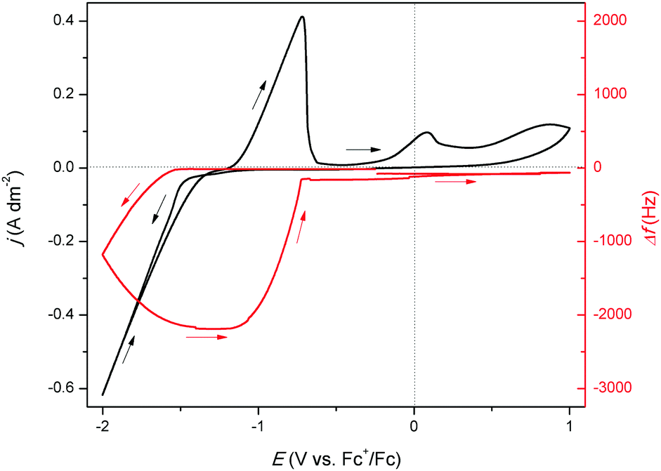
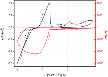
To further investigate the origin of the observed reduction and oxidation features in the CV, an electrochemical quartz crystal microbalance (EQCM) experiment was performed in which a CV is measured while monitoring the frequency response, Δf, of the platinum-coated quartz crystal (Fig. 2). The start of the reduction current at −1.52 V vs. Fc+/Fc is not accompanied by a change in resonance frequency. This indicates that reduction of indium(III) to indium(I) starts at −1.52 V vs. Fc+/Fc. Starting from −1.60 V vs. Fc+/Fc, a decrease in resonance frequency is observed, indicating the deposition of indium due to the further reduction of the indium(I) to indium(0), but also the reduction of indium(III) to indium(0). This can be derived from the E0 values of reactions (2)–(4). The reason why the reduction of indium(III) to indium(I) is possible without the immediate further reduction of the indium(I) to indium(0) (cf. the standard reduction potentials of (3) and (4)) is due to the fact the reduction to indium(0) involves the nucleation of a new phase and hence requires an additional overpotential. The Fc+/Fc couple exhibits a potential of +0.40 V vs. SHE, therefore, reduction of indium(III) to indium(I) would in principle already initiate at −0.843 V vs. Fc+/Fc instead of the observed −1.52 V vs. Fc+/Fc. This discrepancy in onset potential can be attributed to the fact that the experiments were not measured in standard conditions, but also can be due to the coordination of the indium species in the organic electrolyte. Complexation of metal ions can greatly affect the values of redox potentials.26 The resonance frequency continues to decrease until a potential of −1.32 V vs. Fc+/Fc in the backward scan is reached. Between −1.32 V vs. Fc+/Fc and −1.20 V vs. Fc+/Fc, the frequency remains constant, after which it increases to approximately −150 Hz. This increase of Δf overlaps with the oxidation peak in the CV, implying that it corresponds to the stripping of deposited indium. However, as the signal does not fully fall back to zero, not all indium is stripped. Instead, a small quantity of deposited indium alloyed the platinum electrode of the EQCM crystal.27 Consequently, the small peak at +0.10 V vs. Fc+/Fc is attributed to the stripping of the indium–platinum alloy, since it leads to a small increase in frequency, indicating a minor loss of mass. The amount of deposited indium was determined using the following equation:
where Δ
f (Hz) is the change in the resonance frequency of the crystal (working electrode) due to the change in mass Δ
m (kg m
−2) of the crystal;
Cf (kg Hz
−1 m
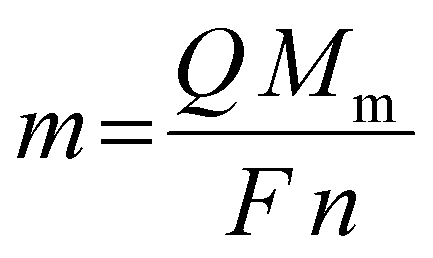
−2) is the calibration constant. Furthermore, the theoretically deposited mass was calculated using Faraday's law:
| |  | (6) |
where
m is the mass (kg),
Q is the fully accumulated charge during reduction (
C),
Mm the molar mass of indium (0.1148 kg mol
−1),
F is the Faraday constant (96485.3 C mol
−1) and
n is the number of electrons involved in the reduction reaction (3, dimensionless). By taking the ratio of the theoretically deposited mass and the experimentally observed mass, the cathodic current efficiency (CCE) is obtained, and equals 94%. Hence, approximately 6% of the total charge generated during reduction is lost. It is assumed that this involves the formation of indium(
I), which does not further reduce to indium(0). Furthermore, the approach for determining the CCE was also applied for calculating the mass change corresponding to the stripping of the formed indium–platinum alloy. The values calculated from the frequency change and from the accumulated charge, integrated from the small oxidation peak approximated each other, equaling around 3.5 × 10
−9 kg. This corresponds to roughly 8 monolayers of indium. The obtained QCM data were used to construct an
M/z vs. potential plot, which is shown in Fig. S1, ESI.
† From this figure it is evident that both reduction to indium(0) and indium(
I) occur, whereas stripping of indium involves oxidation to indium(
I).
 |
| | Fig. 2 CV of 0.25 mol dm−3 of In(CH3SO3)3 in DMSO on a 5 MHz platinum-coated quartz crystal (12.4 mm diameter) at 26 °C with a scan rate of 10 mV s−1 (black line left axis) with EQCM analysis (red line right axis). | |
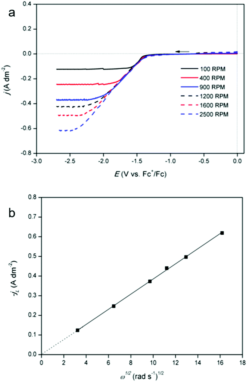
Furthermore, linear sweep voltammograms (LSVs) were recorded for cathodic overpotentials at various rotation rates for a solution of 12.5 mmol dm−3 of indium(III) methanesulfonate and 0.25 mol dm−3 of tetrabutylammonium methanesulfonate in DMSO (Fig. 3a). Compared to the solution used for QCM analysis, the indium content is lower by a factor of 20, in order to reach a diffusion-limited current during the reduction process. The LSVs are utilized to construct a Levich plot (Fig. 3b). This plot shows a linear relation between the limiting currents and the square root of the various rotation rates, and the line intercepts the vertical axis at zero current. As the observed limiting currents in the LSVs are attributed to the reduction of indium(III) to indium(0), the slope of the Levich plot can be used to calculate the diffusion constant of the indium(III) species:
| | | IL = 0.620nFAD2/3ν−1/6C ω1/2 | (7) |
where
IL is the limiting current from the LSV,
n is the number of electrons transferred (3, dimensionless),
F is the Faraday constant (96485.33 C mol
−1),
A is the surface area of the electrode (23.75 × 10
−6 m
2),
D is the diffusion coefficient of the electroactive species (m
2 s
−1),
ν is the kinematic viscosity of the electrolyte (2.1 × 10
−6 m
2 s
−1),
C is the concentration of indium in the electrolyte (12.5 mol m
−3) and
ω is the rotation rate of the electrode (rad s
−1). Using the Levich equation, it is found that the diffusion coefficient of indium(
III) in the diluted solution equals 2.2 × 10
−10 m
2 s
−1 at 26 °C. Reported diffusion coefficients of indium(
III) in aqueous 2 mol dm
−3 NaCl solution at 25 °C and in choline chloride based deep eutectic solvent at 60 °C are 4.93 × 10
−10 m
2 s
−1 and 3.4 × 10
−12 m
2 s
−1, respectively.
28,29 Differences can be attributed by variations in dynamic viscosity of the solution and the hydrodynamic radius of the indium species.
30
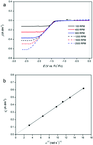 |
| | Fig. 3 (a) LSVs of 12.5 mmol dm−3 of In(CH3SO3)3 and 0.25 mol dm−3 of tetrabutylammonium methanesulfonate in DMSO on a platinum rotating disk electrode (RDE) (diameter of 5.5 mm) at 26 °C, recorded with a scan rate of 10 mV s−1 between 0.0 V and 2.7 V vs. Fc+/Fc and (b) Levich plot constructed from the data of the LSVs. The limiting currents were chosen at a potential of −2.70 V vs. Fc+/Fc in the LSVs. | |
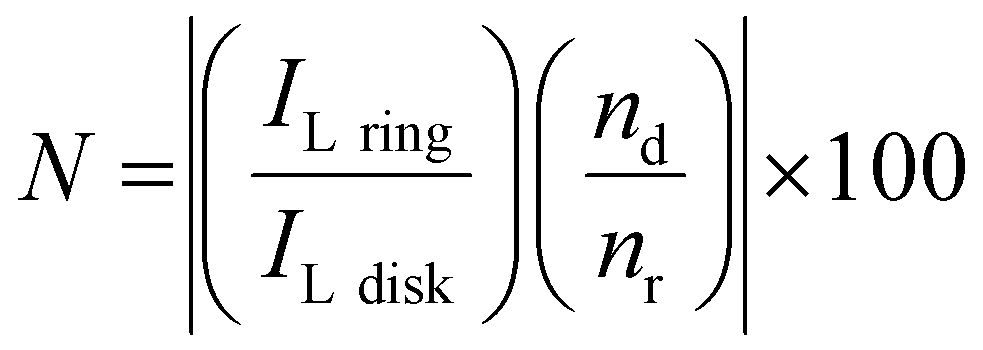
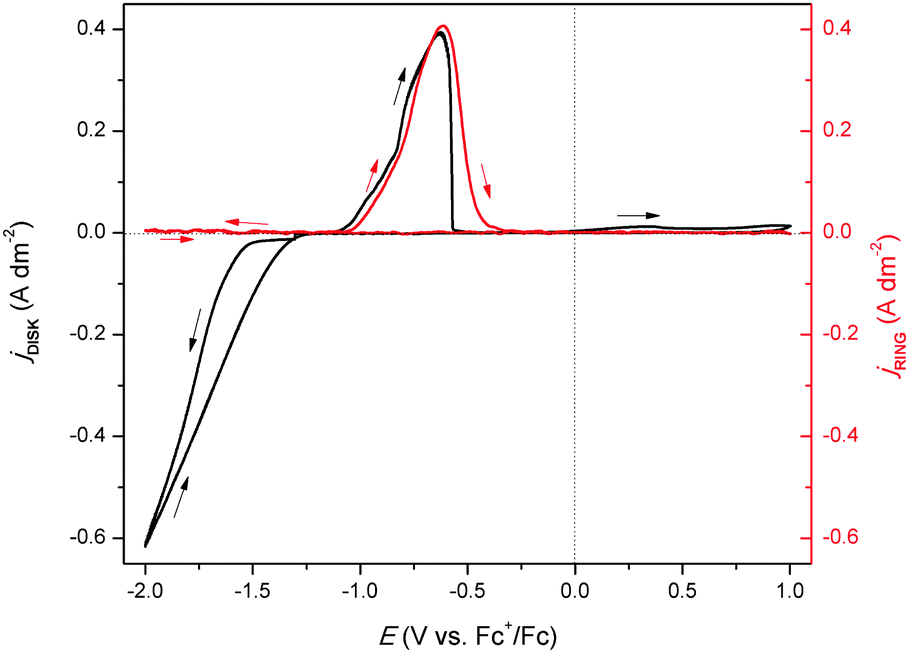
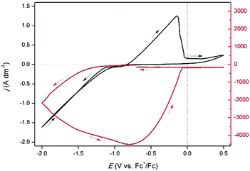
To further study the formation of indium(I) during stripping, a rotating ring disk electrode (RRDE) experiment was performed. This involved the measurement of a CV on the platinum disk, whereas a constant potential of +0.50 V vs. Fc+/Fc was applied on the gold ring, while rotating at 200 rpm. In principle, indium(I), formed during the recording of the CV at the central disk is spun outwards towards the ring and subsequently oxidized to indium(III). In Fig. 4, the resulting measurement is presented, and demonstrates that indium(I) is indeed formed during stripping. Hence, the oxidation peak in the CVs can be ascribed to the oxidation of indium to indium(I). Notably, both the ring current density and the disk current density reach a value of approximately 0.40 A dm−2. As the corresponding process on the disk involves a one-electron process (indium(0) to indium(I)) and that on the ring a two-electron process (indium(I) to indium(III)), the collection efficiency (N) of indium(I) on the ring can calculated using the following equation:
| | 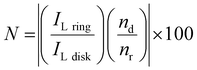 | (8) |
where
ILring and
ILdisk are the limiting ring and disk currents, respectively, and
nd and
nr the number of electrons exchanged in the processes on the disk and ring, respectively. For the performed measurement, the collection efficiency
N was found to be 26%. The maximum capture efficiency of the RRDE was experimentally determined using a ferricyanide solution and found to be 35% (Fig. S2, ESI
†). Hence, about 75% of all indium(
I) is captured on the ring. The indium(
I) species which are not oxidized to indium(
III) on the ring likely underwent the following disproportionation reaction:
 |
| | Fig. 4 RRDE experiment in which the disk (black line left axis) and ring (red line right axis) currents were recorded in 0.25 mol dm−3 of In(CH3SO3)3 in DMSO at 200 rpm at 26 °C. The disk current was generated from the cyclic voltammetry with a scan rate of 10 mV s−1, while the ring was kept at a potential of +0.5 V vs. Fc+/Fc. | |
The occurrence of this reaction has been demonstrated in a number of studies, and also explains the absence of a second oxidation peak involving oxidation of indium(I) to indium(III) in the CVs, as all formed indium(I) reacts away through (9).12,19,20,31
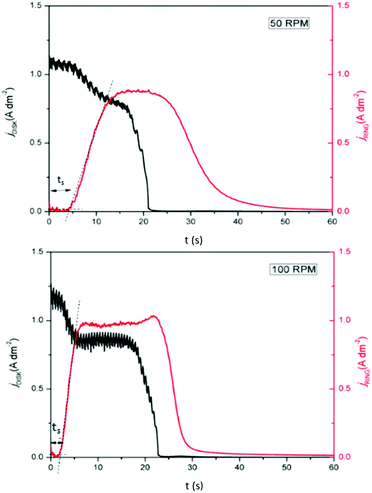
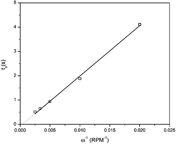
Furthermore, a minor increase in ring current density is observed during the reduction segment of the CV (a magnified image of the cathodic region of the CV with the ring current can be found in Fig. S3, ESI†). Hence, a small quantity of indium(I) is formed. This is in agreement with the observations made from the QCM experiment. Only a small quantity of indium(I) is captured on the ring as the ring current density is very low. This is expected, since the standard reduction potential of indium(I)/indium(0) is lower than that of indium(III)/indium(I). Hence, nearly all indium(I) is further reduced to indium(0) on the disk instead of being spun outwards towards the ring. In RRDE measurements, the time required for a species to travel from the disk to the ring is referred to as the transit time, ts, Using this transit time, the diffusion coefficient of the formed indium(I) species can be found.32 In a first step, a layer of indium is electrodeposited on the disk in stationary conditions by applying a potential of −2.0 V vs. Fc+/Fc for 1 min. Subsequently, the RRDE is rotated at various rotation speeds at which the thin layer of deposited indium is stripped by applying a potential of +0.1 V vs. Fc+/Fc, while a potential of +0.5 V vs. Fc+/Fc is applied on the ring to oxidize the captured indium(I) to indium(III). In Fig. 5, the corresponding stripping currents of the disk, the ring currents, and transit times at 50 rpm and 100 rpm are shown. Furthermore, a plot is constructed showing the linear correlation between the transit time and the reciprocal of the rotational speed is presented in Fig. 6. Evidently, the transit time decreases with increased rotation speeds. The diffusion constant can be calculated using the following equation:33
| | 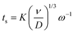 | (10) |
where
ν is the kinematic viscosity of the solution (m
2 s
−1),
D is the diffusion constant (m
2 s
−1),
ω the rotational speed (rpm) and
K is a proportionality constant that depends on the geometry of the RRDE:
K = 43.1[log(
r2/
r1)]
2/3 where
r1 is radius of the disk and
r2 is the inner radius of the ring surrounding the disk. For the RRDE used here,
r1 = 2.75 mm,
r2 = 3.25 mm, and the theoretical value of
K equals 7.49. The kinematic viscosity was determined from the experimentally determined dynamic viscosity and density, and equals 7.0 × 10
−6 m
2 s
−1 (at 26 °C). The diffusion coefficient of indium(
I) was calculated from the slope of the linear fit of
Fig. 6 and equals 3.4 × 10
−10 m
2 s
−1. A table with the transient times for each rotation rate is presented in ESI,
† Table S1.
 |
| | Fig. 5 RRDE experiment in which the disk (black line left axis) and ring (red line right axis) currents were recorded in 0.25 mol dm−3 of In(CH3SO3)3 in DMSO at various rotation speeds, at 26 °C. The disk current was generated from stripping a thin layer of indium, predeposited by applying −2.0 V vs. Fc+/Fc for 1 min, and the ring was kept at a potential of +0.5 V vs. Fc+/Fc. | |
 |
| | Fig. 6 Relation between the inverse of the rotation speed and the transient time. Values for the transient time at various rotation speeds were determined from RRDE experiments at which indium was deposited by applying −2.0 V vs. Fc+/Fc for 1 min on the disk and subsequently stripped by applying +0.1 V vs. Fc+/Fc, while the potential of the ring was kept at +0.5 V vs. Fc+/Fc, using a solution comprised of 0.25 mol dm−3 of In(CH3SO3)3 in DMSO, at 26 °C. | |
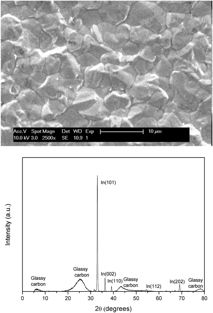
Indium was deposited on a glassy carbon (GC) electrode from 0.25 mol dm−3 of indium(III) methanesulfonate in DMSO at 26 °C by applying −2.0 V vs. Fc+/Fc for 30 min. The morphology and elemental composition were characterized using SEM, EDX and XRD. The resulting image and diffractogram are shown in Fig. 7 (EDX spectrum in ESI,† Fig. S4). The obtained deposit appears to be smooth, consists of pure indium and exhibits a strong preference for the (101) orientation. XRD also reveals minor diffraction peaks for (002), (101), (112) and (202). The observed broader peaks can all be attributed to the GC substrate.34 Assuming the experimentally determined cathodic current efficiency of 94% for the reduction of indium(III) to indium(0), the average theoretical thickness equals approximately 3 μm.
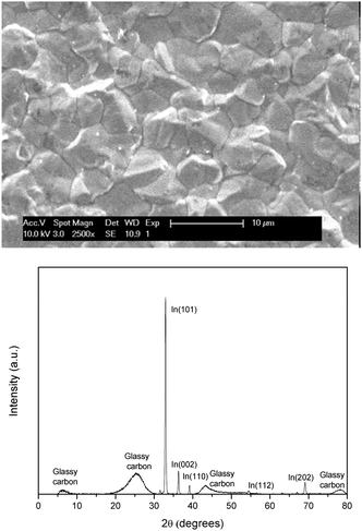 |
| | Fig. 7 SEM image and XRD diffractogram of indium electrodeposited on a GC substrate (80 mm2) at −2.0 V vs. Fc+/Fc at 26 °C. The applied acceleration voltage was 10 keV. | |
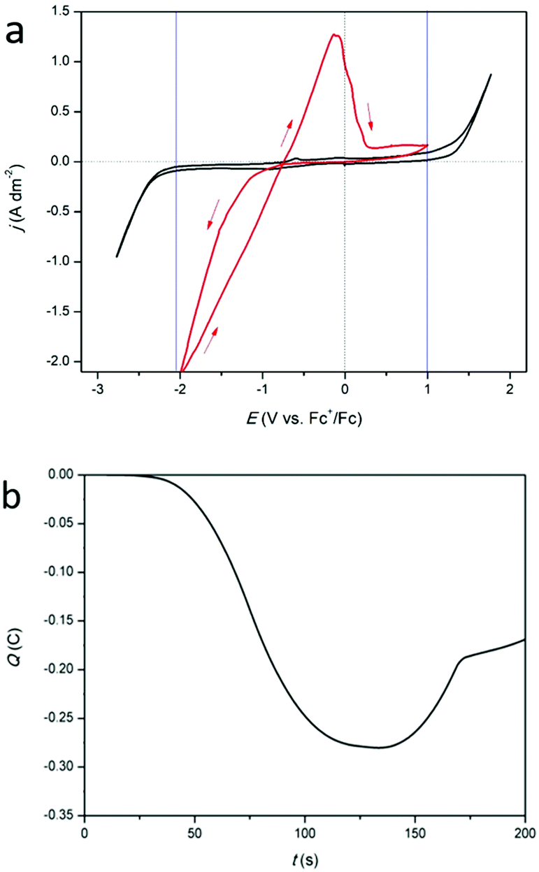
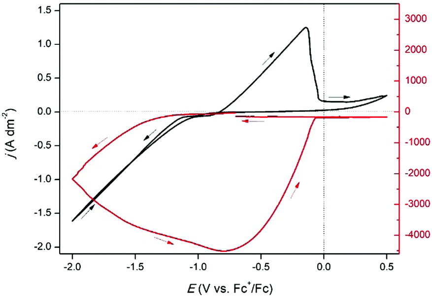
CVs of DMSO with 0.25 mol dm−3 of tetrabutylammonium methanesulfonate (black) and DMSO with 0.25 mol dm−3 of indium(III) methanesulfonate (red), measured at 160 °C, are shown in Fig. 8a. At this temperature the cathodic and anodic breakdown of DMSO occur at −2.00 V vs. Fc+/Fc and +0.94 V vs. Fc+/Fc, respectively (indicated by the blue lines). Clearly, the electrochemical window shrinks with increasing temperature. For the indium-containing solution, an onset in reduction current density is observed at −1.04 V vs. Fc+/Fc. At −2.0 V vs. Fc+/Fc, the current density reaches over −2.0 A dm−2. This is nearly four times higher than observed at 26 °C (Fig. 1a). The increased current density at 160 °C can be attributed to the lower viscosity of the solution, which enables higher mass transport rates of indium(III) species towards the electrode (viscosity vs. temperature plot for the investigated solution in Fig. S5, ESI†). Furthermore, the electrochemical reduction of indium(III) to indium(0) is a chemical reaction, so increasing the temperature will also increase the reaction rate, and therefore the current density. In the backward scan, a single stripping peak is observed at −1.08 V vs. Fc+/Fc, followed by a minor oxidation wave. As the observed reduction and oxidation features in the CV are comparable to those observed at 26 °C, and the charge consumed during oxidation is once more approximately one third of that consumed during reduction (Fig. 8b), the occurring redox reactions are likely similar in nature. Hence, the according reduction processes are expected to involve reduction of indium(III) to indium(I), and to indium(0), whereas the according oxidation process involves stripping of indium(0) to indium(I), and possible stripping of the formed indium–platinum alloy.
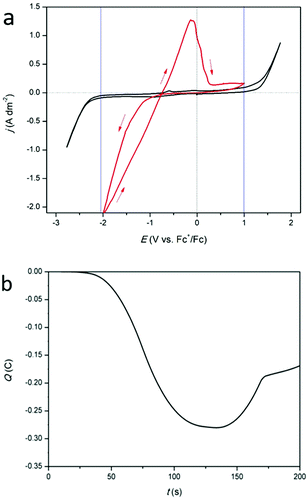 |
| | Fig. 8 (a) CVs of 0.25 mol dm−3 tetrabutylammonium methanesulfonate in DMSO (black) and of 0.25 mol dm−3 of In(CH3SO3)3 in DMSO (red) on a platinum WE (1 mm diameter) at a scan rate of 10 mV s−1 at 160 °C. (b) Coulombic charge as a function of time, derived from the CV (red) in (a). | |
A QCM experiment was performed in which a CV of 0.25 mol dm−3 of indium(III) methanesulfonate in DMSO was measured at 160 °C, while monitoring the frequency response of the platinum-coated quartz crystal (Fig. 9). Upon initiation of the reduction current, the resonance frequency gradually decreases and continues to decrease until −0.72 V vs. Fc+/Fc in the backward scan. This indicates that indium deposition occurs by reduction of indium(III) to indium(0), and possibly of indium(I) to indium(0). After −0.72 V vs. Fc+/Fc, an oxidation current arises and Δf starts to increase until −0.11 V vs. Fc+/Fc. This increase in Δf overlaps with the oxidation peak in the CV, implying that it corresponds to stripping of deposited indium. However, as the signal does not fully fall back to zero, not all indium is stripped. Instead, a small quantity of deposited indium is assumed to have alloyed the platinum electrode of the EQCM crystal. In contrast to the observations at 26 °C, this alloy is not stripped.
 |
| | Fig. 9 CV of 0.25 mol dm−3 of In(CH3SO3)3 in DMSO on a 5 MHz platinum-coated quartz crystal (12.4 mm diameter) at 160 °C with a scan rate of 10 mV s−1 (black line left axis) with EQCM analysis (red line right axis). | |
The CCE of indium deposition was determined by comparing the exact deposited mass, calculated from Δf, and the theoretical mass, calculated from the charge obtained by integrating the reduction current, and equals 76%. This is substantially lower than what is found at 26 °C. The remaining 24% of the reduction current likely went to reduction of indium(III) to indium(I), which did not further reduce to indium(0), but disproportionated in the bulk of the solution. This implies that significantly more indium(I) is formed during reduction at 160 °C as opposed to 26 °C, which is agreement with the findings in our previous study.19 Yet, a notable difference is that in the earlier investigated system, almost no reduction to indium(0) occurred at 160 °C. Indium(III) is nearly completely reduced to indium(I), which disproportionated and resulted in the formation of indium nanoparticles, whereas in this study, about three quarters of the reduction current went to the deposition of indium metal.
A deposition experiment was carried out in which indium was deposited on a GC electrode from 0.25 mol dm−3 of indium(III) methanesulfonate in DMSO at 160 °C by applying −2.0 V vs. Fc+/Fc for 30 min. The obtained deposit was analyzed using SEM, EDX and XRD. The resulting SEM image and diffractogram are found in Fig. 10 (EDX spectrum in Fig. S6, ESI†). The deposit consists of spherical droplets which have wrinkles on their surface. The preferred crystal orientation is (110), whilst another smaller diffraction peak is observed for the (101) plane. The broad peaks can be attributed to the GC substrate. These wrinkles probably form during solidification of the liquid indium droplets. If the point of last solidification occurs on the surface, the molten indium droplets shrink due to the increase in the density of indium upon solidification, causing the appearance of vein-like features. The average theoretical thickness equals 8 μm, considering the CCE of 76%.
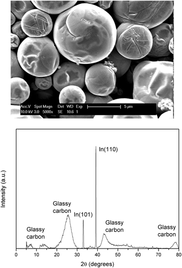 |
| | Fig. 10 SEM image and XRD diffractogram of indium electrodeposited on a GC substrate (105 mm2) at −2.0 V vs. Fc+/Fc at 160 °C for 30 min. From 0.25 mol dm−3 of In(CH3SO3)3 in DMSO. The applied acceleration voltage was 10 keV. | |
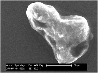 |
| | Fig. 11 SEM image of indium ‘chunk’ found in solution after stripping of indium at +0.1 V vs. Fc+/Fc during 1 hour. The indium was predeposited by applying −2.0 V vs. Fc+/Fc for 2 hours on a GC substrate (20 mm2) at 26 °C. The applied acceleration voltage was 25 keV. | |
Finally, experiments were performed to investigate the disproportionation reaction. Herein, indium was deposited from 0.25 mol dm−3 of indium(III) methanesulfonate in DMSO at 26 °C by applying a potential of −2.0 V vs. Fc+/Fc for 2 hours on a GC substrate (area of 20 mm2). Subsequently, a potential of +0.10 V vs. Fc+/Fc was applied for 1 hour, stripping the deposited indium from the substrate. As the RRDE experiments indicated, stripping involves oxidation of indium(0) to indium(I). As no distinctive oxidation feature is observed in the CVs that can be attributed to the further oxidation of indium(I) to indium(III), indium(I) must undergo a reaction, i.e., the disproportionation reaction shown in eqn (9). During stripping, the measured current drops to zero, indicating complete oxidation of indium(0) (Fig. S7, ESI†). Visual inspection revealed that the indium coating was indeed completely removed from the substrate after the experiment. Interestingly, the solution now contained a large amount of small ‘chunks’ (Fig. S8, ESI†). These were removed from the solution, washed and investigated using SEM and EDX analysis (Fig. 11 and Fig. S9, ESI†). Results show micrometer-sized particles of pure indium. It is postulated that these particles are formed by the disproportionation of indium(I).
Conclusions
In this work, a new non-aqueous electrolyte for the electrodeposition of indium was developed. The precursor, indium(III) methanesulfonate, was synthesized from methanesulfonic acid and indium(III) oxide, and was dissolved in DMSO. The cyclic voltammogram of the prepared electrolyte exhibited a reduction wave and an oxidation peak. QCM analysis and RRDE measurements demonstrated that the according processes were reduction of indium(III) to indium(I), followed by indium(I) to indium(0) and indium(III) to indium(0). Stripping involved oxidation of indium(0) to indium(I). Indium(I) disproportionated in the bulk of the electrolyte, creating micrometer-sized indium metal chunks. Electrodeposition of indium at room temperature led to deposits that were smooth, flat layers, whereas at 160 °C, spherical droplets were obtained. XRD indicated that the deposits were crystalline. The diffusion constants of indium(III) in dilute solutions and of indium(I) were determined using rotating (ring) disk electrodes, equaling 2.2 × 10⁻¹⁰ m2 s−1 and 3.3 × 10⁻¹⁰ m2 s−1 at 26 °C respectively.
Conflicts of interest
There are no conflicts to declare.
Acknowledgements
WM thanks the Research Foundation Flanders (FWO) for a PhD grant (1SB8319N). The research was supported by the European Research Council (ERC) under the European Union's Horizon 2020 Research and Innovation Programme: Grant Agreement 694078 – Solvometallurgy for critical metals (SOLCRIMET). The authors also want to thank Palan Subramanian for sharing his knowledge and insight regarding RRDE measurements.
Notes and references
-
U. Schwarz-Schampera and P. M. Herzig, Indium: geology, mineralogy, and economics, Springer Science & Business Media, 2002 Search PubMed.
-
F. Ullmann, W. Gerhartz, Y. S. Yamamoto, F. T. Campbell, R. Pfefferkorn and J. F. Rounsaville, Ullmann's encyclopedia of industrial chemistry, VCH Publishers, 1985 Search PubMed.
- R. N. Bhattacharya, Sol. Energy Mater. Sol. Cells, 2013, 113, 96–99 CrossRef CAS.
- H. N. Kang, J.-Y. Lee and J.-Y. Kim, Hydrometallurgy, 2011, 110, 120–127 CrossRef CAS.
- A. M. Alfantazi and R. R. Moskalyk, Miner. Eng., 2003, 16, 687–694 CrossRef CAS.
- I. M. Dharmadasa and J. Haigh, J. Electrochem. Soc., 2006, 153, G47–G52 CrossRef CAS.
- R. Piercy and N. A. Hampson, J. Appl. Electrochem., 1975, 5, 1–15 CrossRef CAS.
- F. C. Walsh and D. R. Gabe, Surf. Technol., 1979, 8, 87–99 CrossRef CAS.
- M. Pourbaix and J. Burbank, J. Electrochem. Soc., 1964, 111, 14C CrossRef.
-
W. M. Haynes, CRC handbook of chemistry and physics, CRC Press, 2014 Search PubMed.
- C. Deferm, J. C. Malaquias, B. Onghena, D. Banerjee, J. Luyten, H. Oosterhof, J. Fransaer and K. Binnemans, Green Chem., 2019, 21, 1517–1530 RSC.
- M. K. Carpenter and M. W. Verbrugge, J. Mater. Res., 1994, 9, 2584–2591 CrossRef CAS.
- U. Anders and J. A. Plambeck, Can. J. Chem., 1969, 47, 3055–3060 CrossRef CAS.
- Y.-C. Liu, Y.-C. Chen, Y.-T. Hsieh and I.-W. Sun, J. Phys. Chem. C, 2017, 121, 8907–8913 CrossRef CAS.
- J. Estager, P. Nockemann, K. R. Seddon, G. Srinivasan and M. Swadźba-Kwaśny, ChemSusChem, 2012, 5, 117–124 CrossRef CAS.
- Y. Traore, S. Legeai, S. Diliberto, G. Arrachart, S. Pellet-Rostaing and M. Draye, Electrochim. Acta, 2011, 58, 532–540 CrossRef CAS.
- M. Yang and I. Sun, J. Chin. Biochem. Soc., 2004, 51, 253–260 CrossRef CAS.
- E. Barrado, S. García, J. A. Rodriguez and Y. Castrillejo, J. Electroanal. Chem., 2018, 823, 106–120 CrossRef CAS.
- W. Monnens, C. Deferm, J. Sniekers, J. Fransaer and K. Binnemans, Chem. Commun., 2019, 55, 4789–4792 RSC.
- C. Deferm, J. Luyten, H. Oosterhof, J. Fransaer and K. Binnemans, Green Chem., 2018, 20, 412–424 RSC.
- S. F. Parker and L. Zhong, R. Soc. Open Sci., 2018, 5, 171574 CrossRef.
- F. E. Genceli Guner, M. Lutz, T. Sakurai, A. L. Spek and T. Hondoh, Cryst. Growth Des., 2010, 10, 4327–4333 CrossRef CAS.
- E. M. Arico, L. B. Zinner, B. Kanellakopulos, E. Dornberger, J. Rebizante and C. Apostolidis, J. Alloys Compd., 2001, 323, 39–44 CrossRef.
- K. K. Yang, M. R. Mahmoudian, M. Ebadi, H. L. Koay and W. J. Basirun, Metall. Mater. Trans. B, 2011, 42, 1274–1279 CrossRef CAS.
-
H. Lund and O. Hammerich, Organic electrochemistry, Marcel Dekker, New York, 2001, vol. 4 Search PubMed.
- T. L. Theis and P. C. Singer, Environ. Sci. Technol., 1974, 8, 569–573 CrossRef CAS.
-
W. G. Moffatt, The handbook of binary phase diagrams, 1978 Search PubMed.
- J. C. Malaquias, M. Steichen, M. Thomassey and P. J. Dale, Electrochim. Acta, 2013, 103, 15–22 CrossRef CAS.
- K. Avchukir, B. D. Burkitbayeva, F. Vacandio, A. M. Argimbayeva and G. Rakhymbay, J. Electroanal. Chem., 2019, 842, 176–183 CrossRef CAS.
-
W. B. Russel, W. B. Russel, D. A. Saville and W. R. Schowalter, Colloidal dispersions, Cambridge University Press, 1991 Search PubMed.
- B. Miller and R. E. Visco, J. Electrochem. Soc., 1968, 115, 251–258 CrossRef CAS.
- J. Herranz, A. Garsuch and H. A. Gasteiger, J. Phys. Chem. C, 2012, 116, 19084–19094 CrossRef CAS.
- S. Bruckenstein and G. A. Feldman, J. Electroanal. Chem., 1965, 9, 395–399 CAS.
- T. Noda and M. Inagaki, Bull. Chem. Soc. Jpn., 1964, 37, 1534–1538 CrossRef CAS.
Footnote |
| † Electronic supplementary information (ESI) available: Determination of maximum experimental collection efficiency, charge vs. time plot, m/z plot, a plot showing the stripping current, EDS spectra and SEM images of indium deposits and indium “chunks”. See DOI: 10.1039/d0cp03277h |
|
| This journal is © the Owner Societies 2020 |
Click here to see how this site uses Cookies. View our privacy policy here. 
 Open Access Article
 This Open Access Article is licensed under a Creative Commons Attribution-Non Commercial 3.0 Unported Licence
 a,
Clio
Deferm
a,
Clio
Deferm