
 Open Access Article
 This Open Access Article is licensed under a
 Creative Commons Attribution 3.0 Unported Licence
Noncovalent passivation of supported phosphorene for device applications: from morphology to electronic properties†
Andrea
Lorenzoni
a,
Matteo
Baldoni
 ab,
Elena
Besley
b and
Francesco
Mercuri
*a
ab,
Elena
Besley
b and
Francesco
Mercuri
*a
aIstituto per lo Studio dei Materiali Nanostrutturati (ISMN), Consiglio Nazionale delle Ricerche (CNR), Via P. Gobetti 101, 40129 Bologna, Italy. E-mail: francesco.mercuri@cnr.it; Fax: +39 051 639 8540; Tel: +39 051 639 8518
bDepartment of Physical and Theoretical Chemistry, School of Chemistry, University of Nottingham, University Park, Nottingham NG7 2RD, UK
First published on 26th May 2020
Abstract
An interface between poly(methyl-methacrylate) PMMA-supported phosphorene and layers of linear alkane chains has been studied computationally to reveal an efficient route to noncovalent passivation in terms of the effective coverage of surface area. The formation of strongly ordered compact planar aggregates of alkanes driven by the anisotropy of the phosphorene surface greatly improves the packing at the interface. Small mechanical deformations of the phosphorene structure induced by the interaction with PMMA substrate, a polymer dielectric material, do not alter substantially the mechanical, electronic properties of phosphorene. This indicates remarkable possibilities of using alkanes for prevention of phosphorene from surface degradation phenomena and suggests new technological routes for the fabrication of phosphorene-based electronic devices.
1 Introduction
Phosphorene, an emerging two-dimensional (2D) material, structurally equivalent to a single layer of black phosphorus (BP), has been shown to exhibit many extraordinary physical properties originating from its unique anisotropy in structure.1–3 Similar to other layered materials such as graphite, BP is composed of vertically stacked 2D atomic sheets, held together by weak van der Waals interlayer interactions.2,3 The interlayer separation ranges between 3.21 Å and 3.73 Å4,5 making BP suitable for mechanical exfoliation as in the production of graphene and transition metal dichalcogenide (TMD) layers.2,6,7 Many characteristic features of phosphorene are related to the surface morphology of BP, including strong in-plane anisotropy, which, unlike other layered materials, is reflected in its electronic, thermal and mechanical properties.2,3,8 In BP, the sp3 hybridization leads to localization of a lone pair of electrons on phosphorus atoms, which results in puckering of individual layers and the asymmetric P–P intra-layer bonding pattern. The bonding asymmetry in phosphorene layers is commonly described in terms of armchair (AC) and zigzag (ZZ) directions, defined by the orthogonal vectors in the crystal unit cells.2,3 Another useful property of phosphorene is the presence of a sizeable direct electronic band gap, which has been estimated to be about 1.5 eV,2,3 thus much larger than in BP (0.3 eV).2,3 This hints to a tunability of the electronic band gap in few-layer phosphorene materials, enabling a wide range of applications in electronics and optoelectronics. The large, tunable electronic band gap and high hole mobilities at room temperature (up to 103 cm2 V−1 s−1)2,3,9,10 render phosphorene an ideal candidate as the active material for field-effect devices. Previous work has demonstrated the possibility of fabricating field-effect transistors (FETs) based on phosphorene, with high on/off ratio and operating in the radiofrequency range, thus outperforming similar devices based on graphene.1–3,10,11 However, a few fundamental issues must still be addressed before the widespread exploitation of phosphorene in large-scale applications can be achieved; the most relevant of these issues concerns intrinsic degradation phenomena.1–3,7,11,12 Indeed, the electron lone pairs exposed on the phosphorene surface are prone to chemical attack by external agents, including for example oxygen, leading to degradation of structural and electronic properties, as observed recently.3,7,13 The surface oxidation processes can be partially circumvented by protecting the phosphorene active layer with an overlying layer of inert materials. A common strategy to phosphorene capping involves encapsulating the active layer with polymers or metal oxides.11,13–17 An alternative, well-established approach to passivation of exposed surfaces relies on capping them with molecular materials, such as alkanes, which is a relatively cheap and scalable approach commonly used in organic electronics.18 The possibility of passivating BP by networks of molecular materials7,19 or by 2D materials, such as graphene or hBN,15,20–22 has been shown to effectively prevent surface oxidation phenomena. Another issue that can potentially alter the performance of phosphorene layers in devices is related to the interactions with substrates at the interface, which can exhibit a morphology far from an ideal planar configuration, thus altering the conformation of the overlying layers. This issue is particularly relevant to FET devices based on phosphorene, where the active layer is placed in a direct contact with dielectric materials, such as polymer or oxide layers, to provide electrical insulation from the gate dielectric. Upon adsorption on substrates, the intrinsic properties of phosphorene are often modified, with respect to those of pristine materials. In this work, modification of the structure, dynamics and the electronic properties of the phosphorene monolayer at the interface with organic materials have been investigated computationally using classical molecular dynamics (MD) and density functional theory (DFT). We focus this analysis on studying how the electronic and thermal transport properties of phosphorene are affected by a passivating, non-covalently bound overlayer of linear alkanes. In particular, we explore the interface of the exposed phosphorene surface with layers of linear alkanes, including pentadecane (C15), triacontane (C30) and pentatetracontane (C45). The interaction between a phosphorene monolayer and a poly(methyl-methacrylate) (PMMA) substrate, broadly used in organic electronics as dielectric layer, has been highlighted to represent a gate dielectric in a bottom-gate transistor architecture.23,24 In addition, the electronic properties of phosphorene and related systems are essentially not affected by the interaction with PMMA,25 which therefore constitutes an ideal, inert dielectric material for device applications. Finally, the properties of the phosphorene monolayer at the interface with a polymer dielectric layer and passivated by alkane layers have been also investigated to provide a model of a phosphorene-based device in a more realistic environment. This configuration mimics a realistic device stack, where the remarkable dielectric properties of polymer materials are coupled to solution processing techniques for passivating phosphorene with ultra-thin layers.2 Computational details
Simulations of the morphology of individual layers and interfaces have been performed using classical molecular dynamics (MD). Phosphorene models were described by the interatomic potential of Sresht et al.26 and the PMMA slab was obtained by applying the OPLS potential,27 as described previously.28 Model systems with a surface area of about 10 × 10 nm were used in calculations. A periodic model of PMMA chains, having 32 monomer units each, was relaxed in MD simulations at room temperature in the NPT ensemble. The relaxed in-plane size of the PMMA slab resulted 9.57 × 10.1 nm, with a thickness of about 5 nm. The simulation protocol of ref. 28 was applied to obtain a final equilibrated structure with lateral periodic dimensions matching those of a phosphorene supercell, thus minimizing lattice mismatch. The surface characteristics of the obtained PMMA slab compare well with typical parameters measured in experiments.28 Standard OPLS parameters were also adopted for alkane Cn (n = 15, 30, 45) molecules. Inter-layer interactions at the PMMA/phosphorene and phosphorene/alkanes interfaces were described by the Lennard-Jones potential with parameters obtained by the geometric mixing rules as these interactions are dominated by van der Waals forces. The application of geometric mixing rules to the description of the interaction between phosphorene and carbon-based materials has proven effective in previous work.29–31 The computed alkane–phosphorene interaction energies are in line with dispersion-corrected DFT calculations (see Fig. S7 in ESI†). In all MD calculations involving phosphorene interfaces, all phosphorus atom were allowed to move. Electrostatic interactions were calculated using the particle–particle particle–mesh (PPPM) method, and the cut-off of 10.0 Å was used for both Coulomb and van der Waals interactions. A time step of 1.0 fs was used in MD simulations with the Nose–Hoover thermostat applied in the canonical (NVT) ensemble with time constant of 0.1 ps and the Parrinello–Rahman barostat used in the NPT ensemble, with a time constant of 1.0 ps. In MD calculations, periodic boundary conditions (PBC) were applied in 3 dimensions, and in simulations of slabs with 2D periodicity a vacuum region ranging from 10 to 20 nm (see below) was added along the z direction. The morphology of alkane aggregates growing on phosphorene under kinetic and thermodynamic control has been simulated by a combination of non-equilibrium and equilibrium MD, as described in previous work.32,33 Initially, amorphous aggregates of alkanes on phosphorene were generated by progressively adding individual alkane chains, relaxed at 300 K, to the phosphorene surface at an interval of 50 ps. Positions of alkane chains on the xy periodic plane were assigned randomly at a distance of 5 nm from the phosphorene surface on the non-periodic z direction. In order to promote the interaction with the surface, a constant factor, ranging from 0.5 to 0.6 nm ps−1, was added to the z-component of the velocity of alkane atoms pointing towards the phosphorene plane. This process was repeated until the target surface coverage was reached. Equilibration of the system at 300 K for 20 ns has reproduced a kinetically-controlled aggregation of alkanes on phosphorene. A model morphology of alkane aggregates on phosphorene layers in thermodynamically-controlled conditions was subsequently obtained by a simulated annealing cycle, which consists of annealing of the system at 400 K at a rate of 0.5 K ps−1, equilibration at 400 K for 10 ns, cooling to 300 K at a rate of 0.2 K ps−1 and the final equilibration at 300 K for 10 ns.The configurations of individual alkane chains on the surface of phosphorene was analyzed in terms of the configurational parameter φ, defined as the angle between the axis connecting the center of mass of two adjacent carbon–carbon bonds, computed for all non-terminal bonds in the chain, and the ZZ direction of the underlying phosphorene layer (see inset of Fig. 3c). The nominal coverage, Θ, of alkanes on phosphorene was defined as the ratio between the total number of alkane chains in the system and the number of alkane chains, in a planar ordered configuration, needed to occupy a surface area equivalent to that of the underlying phosphorene layer. Therefore, Θ = 1.00 corresponds to a nominally complete monolayer (ML) of alkanes on phosphorene. The effective coverage η of the phosphorene layer by alkane chains was defined as the ratio between the surface area occupied by the alkane molecules and the total surface area of the phosphorene layer in the simulation box. The surface occupied by alkane chains was measured by reproducing a surface profile obtained by convolution of all atoms with the van der Waals spheres of 2.0 Å radius, and defining all regions of the surface higher than 4 Å with respect to the phosphorene base plane as covered (see Fig. S1 in ESI†). The root mean square (RMS) roughness of the surfaces was computed by discretizing the model systems in the in-plane directions with a lateral mesh-grid size of 2 Å. The analysis of surface parameters and coverage was performed by using the software package Gwyddion.34 The phonon power spectra of phosphorene layers were simulated by computing the discrete Fourier transform of the velocity autocorrelation function of phosphorous atoms extracted from the equilibrium MD runs performed for 50 ps with a timestep of 0.5 fs. All classical simulations have been performed using the LAMMPS program package.35 Model systems for MD calculations required a number of particles ranging from about 61k to 110k. Density functional theory (DFT) calculations were performed at the gradient-corrected level by applying the PBE36 exchange–correlation functional within the GPW approach37,38 as implemented in the CP2K program package.39 Electronic states were expanded by a double-ζ plus polarisation basis set, DZVP,40 with norm-conserving pseudo-potentials for the description of core levels,41–43 and a plane-wave representation of the charge density with a cut-off of 300 Ry. Calibration calculations performed with larger charge density cut-off energies (up to 500 Ry) provided essentially the same results.
3 Results and discussion
The structural and electronic properties of phosphorene can be affected by the interactions with an underlying substrate. Deposition of exfoliated phosphorene flakes onto substrates can alter the planarity of the layers, depending on the roughness of the underlying materials and on the strength of the phosphorene/substrate interaction, thus potentially altering the electronic properties of phosphorene. To evaluate this, the morphology of phosphorene at the interface with PMMA has been simulated by MD calculations, and subsequently applying DFT on configurations extracted from MD to compute electronic properties. The obtained model of the PMMA surface features a RMS roughness of 0.5 nm, which is comparable with that of PMMA dielectric layers typically used in organic FETs.28A model of a free-standing phosphorene layer with 29 × 23 unit cells, was initially relaxed by variable-cell MD simulations. The relaxed configuration was found to retain a fully planar structure, with an equilibrated lateral size of 9.57 × 10.1 nm. The equilibrated phosphorene monolayer was put in contact with the surface of the PMMA model, with a box size of 20 nm in the out-of-plane direction, and relaxed by MD at room temperature for 10 ns, in the NVT ensemble, to achieve the full equilibration of all structural parameters. As shown in Fig. 1, the equilibrated phosphorene monolayer conforms anisotropically to the underlying PMMA surface with deformations affecting mainly the AC direction, as measured by the surface roughness in the AC direction (0.14 nm) and ZZ direction (0.06 nm). The overall roughness of about 0.16 nm, however, indicates a much smoother profile with respect to that of the underlying PMMA surface.
 | ||
| Fig. 1 (a) MD snapshot of the equilibrated phosphorene monolayer on PMMA and (b) the surface profile. | ||
A comparison of the density of states (DOS) for a model planar phosphorene layer and a supported phosphorene structure extracted from the MD simulations (lateral box size 9.57 × 10.1 nm and box size of 1.4 nm along the direction perpendicular to the surface, with a total of 2668 atoms in the model) was performed by DFT calculations. To this end, the configuration of rippled phosphorene on PMMA was used, evaluating the electronic properties of the phosphorene layer only. Indeed, the electronic properties of phosphorene materials are generally not affected by interaction with PMMA.25 Calculations indicate that the electronic properties of phosphorene are essentially unaffected by the mechanical deformation induced by the interaction with the PMMA substrate. The Highest-Occupied and Lowest-Unoccupied Crystal Orbitals (HOCO and LUCO, respectively), plotted in Fig. 2 at the Γ point, exhibit very similar features for the planar and PMMA supported phosphorene models, and the computed DOS (see Fig. 2e) remains largely unchanged. In particular, a slight increase of the band gap between the valence and conduction bands is observed from planar (0.69 eV) to supported (0.73) phosphorene.
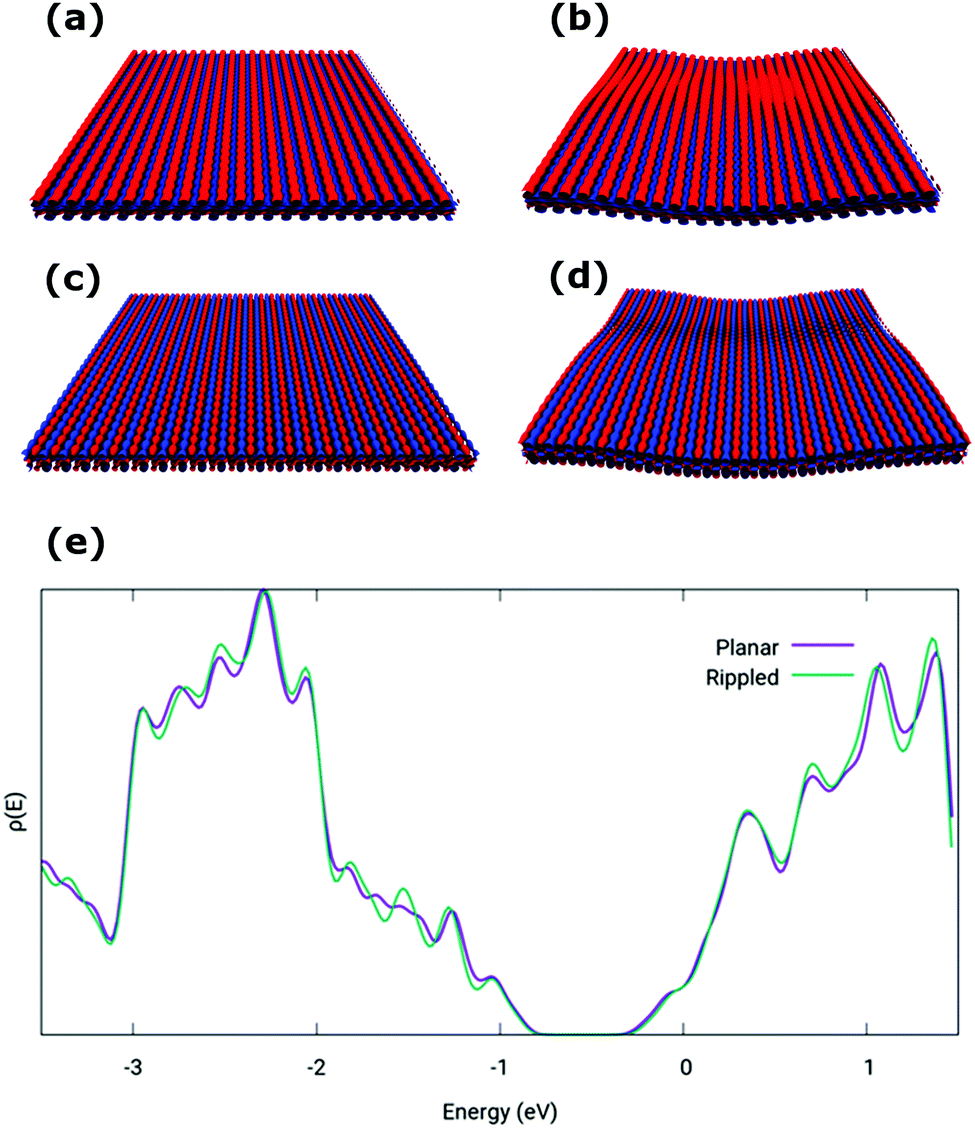 | ||
| Fig. 2 The HOCO (top) and LUCO (bottom) orbitals for a free-standing (a and c) and PMMA supported phosphorene layer (b and d); DOS (e) of a free-standing planar (purple curve) and PMMA supported (green curve) phosphorene. | ||
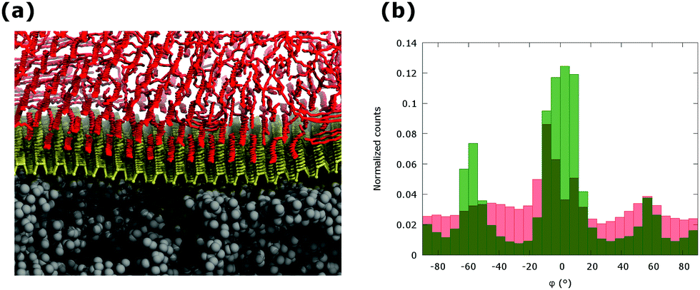
A non-covalent passivation of a phosphorene layer with alkane chains has been initially modelled as an aggregation of alkanes on the surface of a planar, free-standing phosphorene. A computational model for the growth of alkane aggregates on phosphorene in kinetically- and thermodynamically-controlled conditions has been set-up as described above (Computational details section). A relaxed model of the phosphorene layer with lateral sizes of 12.0 × 11.3 nm (36 × 25 unit cells) and a box size of 10 nm in the out-of-plane direction was used. The obtained morphology of the alkane network for the increasing value of the nominal coverage (from Θ = 0.25 to Θ = 2.00) suggests a clear propensity to the formation of ordered aggregates at the interface with phosphorene (see Fig. 3). No significant rippling of the phosphorene surface was observed upon formation of the passivating alkane layer. The ordered morphology indicates an extremely efficient passivation of the phosphorene surface by alkanes, with a striking correspondence between the nominal coverage Θ and the effective coverage η, which deviate by only about 2% (see Fig. S2 and Table S1 in ESI†). At the nominal coverage Θ = 1.00 corresponding to a nominally complete monolayer (1 ML), the effective coverage η is about 0.99, thus indicating an almost full passivation and a strong potential of alkane chains as protective material for phosphorene layers. Remarkably, the effective coverage is essentially independent from the thermal treatments as similar values for η have been obtained for alkane chains relaxed in both kinetically- and thermodynamically-controlled conditions (see Table S1 in ESI†). The different degree of structural ordering for kinetically- and thermodynamically-controlled growth of alkanes on phosphorene is observed in the whole range of nominal coverages considered, from Θ = 0.25 to Θ = 2.00 (see Fig. S2 in ESI†). It is also worth noting that the post-annealing of layers of alkanes grown on phosphorene in strongly kinetically-controlled conditions can lead to efficiently packed structures. These structures, however, exhibit a slightly less pronounced structural ordering with respect to the thermodynamically-controlled growth (see Fig. S3 in ESI†). Also, in the range of the values considered in this work, the effective coverage does not depend on the length of the alkane chain (see Fig. S4 in ESI†). In kinetically-controlled growth conditions – these occur, for example, in solution-phase deposition of alkanes on phosphorene at room temperature – local crystalline ordering of alkane chains is observed (Fig. 3a), with the formation of strongly ordered nanometre sized grains, which are mostly oriented along the ZZ direction of the phosphorene lattice (φ = 0°) and along two equivalent directions of the phosphorene lattice at φ = 55° and φ = −55°, respectively (see Fig. 3c). Upon annealing at a 400 K, and subsequent cooling to room temperature a long-range ordered packing of alkane chains is achieved (see Fig. 3b), with most of the alkane chains oriented along the ZZ direction of phosphorene (see Fig. 3c). The predominance of preferential high-symmetry orientation for alkane layers on phosphorene can be understood by investigating a model system containing a single alkane chain or a small cluster on the phosphorene surface. These calculations indicate a significant interaction energy between alkanes and phosphorene, amounting to 2.75 eV per molecule for a C30 chain, which contributes to the formation of stable aggregates (see Fig. S5a in ESI†). The adsorption energy per molecule further increases as the number of passivating alkanes goes up as a result of the intra-layer lateral chain interactions. The optimised lateral distance between alkane chains in planar aggregates is predicted to be 4.39 Å. This value is remarkably close to the lattice constant of phosphorene in the AC direction, 4.38 Å, which corresponds to the distance between the surface grooves, thus favoring the alignment of alkanes on phosphorene along the ZZ direction in thermodynamically stable aggregates (Fig. S5b in ESI†). The anisotropy of the phosphorene surface and the peculiar match between the underlying lattice and the intrinsic propensity of alkanes to form planar ordered aggregates greatly improve the packing at the interface and lead to the formation of compact passivation layers. Passivation of the exposed surface by a compact layer of weakly-bound molecules prevents the material from chemical degradation and, at the same time, is expected to have a very small impact on the intrinsic properties of phosphorene.
 | ||
| Fig. 3 Morphology of C30 chains on phosphorene at the coverage of Θ = 1.0 as obtained by MD simulations at room temperature (a) and after an annealing/cooling cycle (b). Distribution of the angular parameter (c) for the system relaxed at room temperature (blue bars) and after annealing/cooling cycle (red bars) (inset: definition of the angular parameter φ). | ||
To consider the morphology of a passivating layer of alkanes on supported phosphorene, the deposition of individual C30 alkane chains on a phosphorene monolayer supported on PMMA has been simulated by combining the non-equilibrium and equilibrium MD. The equilibrated model of phosphorene relaxed on PMMA, with lateral box size of 9.57 × 10.1 nm and 20 nm along the z direction was used. The nominal coverage corresponding to approximately five monolayers (5 ML) has been achieved and subsequently equilibrated at room temperature for 10 ns. These simulations correspond to the growth of alkane layers at the interface with supported phosphorene in kinetically controlled conditions. The equilibrated configuration (see Fig. 4a) shows an ordered and anisotropic aggregation of alkanes at the interface, similar to the case of aggregation on planar phosphorene. The C30 molecules, which are in direct contact with the phosphorene surface, are aligned along the three preferential orientations described above (φ = 0° and φ = ±55°). A slight preference is observed for the orientation along the ZZ axis of the phosphorene layer, as supported phosphorene exhibits larger bending along the AC direction. The morphology of PMMA supported phosphorene is unaffected by the overlying aggregate of alkane chains as indicated by the overall roughness, rRMS = 0.17 nm, and by the roughness parameters for specific orientations, rRMSZZ = 0.08 nm and rRMSAC = 0.15 nm, extracted from the equilibrated structure of the sandwiched layer. This behaviour differs from that of alkanes on supported graphene, where a significant change in the surface morphology are observed upon the interaction with the adsorbate.18 However, the anisotropy of the aggregation on PMMA supported phosphorene is only partially retained if the distance from the interface is increased, as shown by the distribution of the angular parameter φ as a function of the distance between the alkane chains and the phosphorene layer (see Fig. 4b). The formation of highly ordered alkane aggregates at the interface leads to the efficient protection of the exposed surface of PMMA supported phosphorene layers. Even at the nominal coverage of 1 ML, the exposed surface of supported phosphorene is less than 5% of the total surface area, thus suggesting an optimal and effective coverage by alkane layers. The presence of passivating layers of alkanes is also expected to have a minimal impact on the electronic properties of phosphorene. Dispersion-corrected DFT calculations indicate an interaction energy of less than 0.1 eV per carbon atom, mostly due to van der Waals interactions (see Fig. S6 and Table S2 in ESI†). The electronic properties of phosphorene supported on PMMA and passivated by alkane layers can therefore be expected to be very similar to those of a pristine phosphorene layer, with a slight effect due to rippling.
 | ||
| Fig. 4 Morphology of C30 chains on phosphorene at the coverage of Θ = 5.0 placed on PMMA substrate as obtained by MD simulations at room temperature (a) and distribution of the angular parameter as a function of the distance from the interface of alkane chains in stacked layered slices (interface: green bars; above interface: red bars) (b). | ||
The changes in the dynamical and transport properties of a phosphorene monolayer induced by the interactions with the PMMA substrate and the passivating layer of alkanes have been further assessed by computing the phonon power spectrum and its in-plane and out-of-plane components (see Fig. 5). The intensity of the low-frequency phonons in the ZZ direction of the phosphorene lattice (top panel in Fig. 5) is slightly lowered as a result of interaction with alkanes (yellow curve); this is expected for the vibration modes of phosphorus atoms aligned with the principal axis of the overlying alkane. Conversely the components of the high-frequency modes in the AC and out-of-plane directions, related to the vibrations of P–P bonds, are slightly enhanced by sandwiching the phosphorene layer between PMMA and the alkane layer (purple curves in Fig. 5). Therefore, the properties related to the phonon spectrum of phosphorene, in the passivated and supported configuration, (including, for example, thermal transport properties), are only marginally different from those of a planar phosphorene monolayer.
 | ||
| Fig. 5 Components of the phonon power spectrum (ZZ direction: top; AC direction: middle; out-of-plane direction: bottom) of phosphorene (orange), phosphorene supported on PMMA (blue), phosphorene interacting with 1 ML alkanes (yellow) and 5 ML alkanes on phosphorene supported on PMMA (purple). | ||
4 Conclusions
Effective protection of phosphorene from severe degradation effects, such as damage by moisture, oxygen in air, molecular diimides and other surface reactions, which make phosphorene unstable in atmosphere, is critical for its practical use in applications including optoelectronic devices. New strategies are emerging to reduce the structural and property degradation using the encapsulation and surface passivation techniques. Previous device concepts have been realized in laboratories in high vacuum environments in order to eliminate the agents causing degradation,9 however the large-scale device implementation requires alternative feasible solutions. The success of encapsulation and coating has been tested in silicene FET protection44 and in protecting the flakes of BP with overlayers of Al2O3.13,17 The non-covalent passivation has shown to provide another efficient route to preserving phosphorene morphology and its electronic, thermal and mechanical properties from the surface degradation effects.19 In this work, we have investigated the phosphorene surface, supported on PMMA and protected by alkane chain layers to show that although phosphorene adopts a slight rippling on a PMMA slab this minor structure deformation does not affect its electronic properties. An effective use of long alkane chains as protection is promising as alkanes tend to form ordered and compact aggregates at the interface with phosphorene. The alkane chains are aligned along three main orientations, which are topologically related to the underlying phosphorene lattice, however the specific orientational distribution depends on the growth conditions and thermal treatment. The difference between the interaction energy in two minima is comparable to the thermal energy at room temperature and only one preferential orientation was observed experimentally.19 In our simulations, upon annealing at 400 K and subsequent cooling to room temperature a long-range ordered packing of alkane chains has been achieved where most of the alkane chains were aligned along the ZZ direction of phosphorene. The overall coverage of the phosphorene layer, however, is not quantitatively affected by the specific arrangement of individual alkane chains at the interface. The properties of a double interface, in which a phosphorene monolayer is sandwiched between a support layer (PMMA) and a protective alkane layer, are largely unaltered as compared to pristine, free-standing phosphorene layers. This conclusion points out some remarkable possibilities of using alkanes as non-covalent passivating layers to prevent phosphorene from surface degradation phenomena and suggests new technological routes for the fabrication of electronic devices based on phosphorene. Although phosphorene is not as stable as graphene and TMD, recent success in protection of unstable materials such as silicene44 suggests that the development of passivation and encapsulation solutions could lead to protection of even vulnerable 2D materials such as phosphorene.Conflicts of interest
There are no conflicts to declare.Acknowledgements
We acknowledge the CINECA award under the ISCRA initiative, for the availability of high performance computing resources and support. We acknowledge the use of Athena at HPC Midlands+, which was funded by the EPSRC on grant EP/P020232/1 as part of the HPC Midlands+ consortium. Computational simulations were also partially performed at the High Performance Computing Facility at the University of Nottingham. EB would like to thank the Royal Society for the award of a Royal Society Wolfson Fellowship.Notes and references
- V. Eswaraiah, Q. Zeng, Y. Long and Z. Liu, Small, 2016, 3480–3502 CrossRef CAS PubMed.
- A. Carvalho, M. Wang, X. Zhu, A. S. Rodin, H. Su and A. H. Castro Neto, Nat. Rev. Mater., 2016, 1, 16061 CrossRef CAS.
- M. Akhtar, G. Anderson, R. Zhao, A. Alruqi, J. E. Mroczkowska, G. Sumanasekera and J. B. Jasinski, npj 2D Mater. Appl., 2017, 1, 5 CrossRef.
- S. Appalakondaiah, G. Vaitheeswaran, S. Lebègue, N. E. Christensen and A. Svane, Phys. Rev. B: Condens. Matter Mater. Phys., 2012, 86, 035105 CrossRef.
- J. Dai and X. C. Zeng, J. Phys. Chem. Lett., 2014, 5, 1289–1293 CrossRef CAS PubMed.
- C. R. Ryder, J. D. Wood, S. A. Wells, Y. Yang, D. Jariwala, T. J. Marks, G. C. Schatz and M. C. Hersam, Nat. Chem., 2016, 8, 597–602 CrossRef CAS PubMed.
- V. V. Korolkov, I. G. Timokhin, R. Haubrichs, E. F. Smith, L. Yang, S. Yang, N. R. Champness, M. Schröder and P. H. Beton, Nat. Commun., 2017, 8, 1–8 CrossRef CAS PubMed.
- F. Xia, H. Wang and Y. Jia, Nat. Commun., 2014, 5, 1–6 Search PubMed.
- L. Li, Y. Yu, G. J. Ye, Q. Ge, X. Ou, H. Wu, D. Feng, X. H. Chen and Y. Zhang, Nat. Nanotechnol., 2014, 9, 372–377 CrossRef CAS PubMed.
- H. Liu, A. T. Neal, Z. Zhu, Z. Luo, X. Xu, D. Tománek and P. D. Ye, ACS Nano, 2014, 8, 4033–4041 CrossRef CAS PubMed.
- J.-S. Kim, Y. Liu, W. Zhu, S. Kim, D. Wu, L. Tao, A. Dodabalapur, K. Lai and D. Akinwande, Sci. Rep., 2015, 5, 8989 CrossRef CAS PubMed.
- B. Wan, Q. Zhou, J. Zhang, Y. Wang, B. Yang, W. Lv, B. Zhang, Z. Zeng, Q. Chen, J. Wang, W. Wang, F. Wen, J. Xiang, B. Xu, Z. Zhao, Y. Tian and Z. Liu, Adv. Electron. Mater., 2018, 1700455, 1700455 CrossRef.
- J. D. Wood, S. A. Wells, D. Jariwala, K. S. Chen, E. Cho, V. K. Sangwan, X. Liu, L. J. Lauhon, T. J. Marks and M. C. Hersam, Nano Lett., 2014, 14, 6964–6970 CrossRef CAS PubMed.
- Y. Y. Illarionov, M. Waltl, G. Rzepa, J. S. Kim, S. Kim, A. Dodabalapur, D. Akinwande and T. Grasser, ACS Nano, 2016, 10, 9543–9549 CrossRef CAS PubMed.
- A. Avsar, I. J. Vera-Marun, J. Y. Tan, K. Watanabe, T. Taniguchi, A. H. Castro Neto and B. Özyilmaz, ACS Nano, 2015, 9, 4138–4145 CrossRef CAS PubMed.
- S. Sinha, Y. Takabayashi, H. Shinohara and R. Kitaura, 2D Mater., 2016, 3, 035010 CrossRef.
- J. Na, Y. T. Lee, J. A. Lim, D. K. Hwang, G. T. Kim, W. K. Choi and Y. W. Song, ACS Nano, 2014, 8, 11753–11762 CrossRef CAS PubMed.
- S. A. Svatek, O. R. Scott, J. P. H. Rivett, K. Wright, M. Baldoni, E. Bichoutskaia, T. Taniguchi, K. Watanabe, A. J. Marsden, N. R. Wilson and P. H. Beton, Nano Lett., 2015, 15, 159–164 CrossRef CAS PubMed.
- M. Bolognesi, M. Brucale, A. Lorenzoni, F. Prescimone, S. Moschetto, V. V. Korolkov, M. Baldoni, M. Serrano-Ruiz, M. Caporali, F. Mercuri, E. Besley, M. Muccini, M. Peruzzini, P. H. Beton and S. Toffanin, Nanoscale, 2019, 11, 17252–17261 RSC.
- R. A. Doganov, E. C. O'Farrell, S. P. Koenig, Y. Yeo, A. Ziletti, A. Carvalho, D. K. Campbell, D. F. Coker, K. Watanabe, T. Taniguchi, A. H. Neto and B. Özyilmaz, Nat. Commun., 2015, 6, 6647 CrossRef CAS PubMed.
- N. Gillgren, D. Wickramaratne, Y. Shi, T. Espiritu, J. Yang, J. Hu, J. Wei, X. Liu, Z. Mao, K. Watanabe, T. Taniguchi, M. Bockrath, Y. Barlas, R. K. Lake and C. N. Lau, 2D Mater., 2015, 2, 1–8 Search PubMed.
- X. Chen, Y. Wu, Z. Wu, Y. Han, S. Xu, L. Wang, W. Ye, T. Han, Y. He, Y. Cai and N. Wang, Nat. Commun., 2015, 6, 1–6 Search PubMed.
- S. Tanida, K. Noda, H. Kawabata and K. Matsushige, Thin Solid Films, 2009, 518, 571–574 CrossRef CAS.
- P. Lutsyk, K. Janus, J. Sworakowski, G. Generali, R. Capelli and M. Muccini, J. Phys. Chem. C, 2011, 115, 3105–3114 CrossRef.
- F. Telesio, E. Passaglia, F. Cicogna, F. Costantino, M. Serrano-Ruiz, M. Peruzzini and S. Heun, Nanotechnology, 2018, 29, 295601 CrossRef PubMed.
- V. Sresht, A. A. H. Pádua and D. Blankschtein, ACS Nano, 2015, 9, 8255–8268 CrossRef CAS PubMed.
- W. L. Jorgensen, D. S. Maxwell and J. Tirado-Rives, J. Am. Chem. Soc., 1996, 118, 11225–11236 CrossRef CAS.
- A. Lorenzoni, M. Muccini and F. Mercuri, RSC Adv., 2015, 5, 11797–11805 RSC.
- Q. X. Pei, X. Zhang, Z. Ding, Y. Y. Zhang and Y. W. Zhang, Phys. Chem. Chem. Phys., 2017, 19, 17180–17186 RSC.
- N. Wei, Y. Chen, Y. Zhang, C. Zhou, X. Hao, K. Xu, K. Cai and J. Chen, Nanoscale, 2018, 10, 4385–4390 RSC.
- V. V. Chaban, E. E. Fileti and O. V. Prezhdo, ACS Nano, 2017, 11, 6459–6466 CrossRef CAS PubMed.
- A. Lorenzoni, M. Muccini and F. Mercuri, Adv. Theory Simul., 2019, 2, 1900156 CrossRef CAS.
- A. Lorenzoni, A. Mosca Conte, A. Pecchia and F. Mercuri, Nanoscale, 2018, 10, 9376–9385 RSC.
- D. Nečas and P. Klapetek, Cent. Eur. J. Phys., 2012, 10, 181–188 Search PubMed.
- S. Plimpton, J. Comput. Phys., 1995, 117, 1–19 CrossRef CAS.
- J. Perdew, K. Burke and M. Ernzerhof, Phys. Rev. Lett., 1996, 77, 3865–3868 CrossRef CAS PubMed.
- G. Lippert, J. Hutter and M. Parrinello, Mol. Phys., 1997, 92, 477–488 CrossRef CAS.
- J. Vandevondele, M. Krack, F. Mohamed, M. Parrinello, T. Chassaing and J. Hutter, Comput. Phys. Commun., 2005, 167, 103–128 CrossRef CAS.
- J. Hutter, M. Iannuzzi, F. Schiffmann and J. VandeVondele, Wiley Interdiscip. Rev.: Comput. Mol. Sci., 2014, 4, 15–25 CAS.
- J. VandeVondele and J. Hutter, J. Chem. Phys., 2007, 127, 114105 CrossRef PubMed.
- S. Goedecker, M. Teter and J. Hutter, Phys. Rev. B: Condens. Matter Mater. Phys., 1996, 54, 1703–1710 CrossRef CAS PubMed.
- C. Hartwigsen, S. Goedecker and J. Hutter, Phys. Rev. B: Condens. Matter Mater. Phys., 1998, 58, 3641–3662 CrossRef CAS.
- M. Krack, Theor. Chem. Acc., 2005, 114, 145–152 Search PubMed.
- L. Tao, E. Cinquanta, D. Chiappe, C. Grazianetti, M. Fanciulli, M. Dubey, A. Molle and D. Akinwande, Nat. Nanotechnol., 2015, 10, 227–231 CrossRef CAS PubMed.
Footnote |
| † Electronic supplementary information (ESI) available. See DOI: 10.1039/d0cp00939c |
| This journal is © the Owner Societies 2020 |