
 Open Access Article
 This Open Access Article is licensed under a Creative Commons Attribution-Non Commercial 3.0 Unported Licence
Large scale indium tin oxide (ITO) one dimensional gratings for ultrafast signal modulation in the visible spectral region†
Michele
Guizzardi
a,
Silvio
Bonfadini
b,
Liliana
Moscardi
ab,
Ilka
Kriegel
c,
Francesco
Scotognella
 *ab and
Luigino
Criante
b
*ab and
Luigino
Criante
b
aDipartimento di Fisica, Politecnico di Milano, Piazza Leonardo da Vinci 32, 20133 Milano, Italy. E-mail: francesco.scotognella@polimi.it
bCenter for Nano Science and Technology@PoliMi, Istituto Italiano di Tecnologia, Via Giovanni Pascoli, 70/3, 20133, Milan, Italy
cDepartment of Nanochemistry, Istituto Italiano di Tecnologia (IIT), via Morego, 30, 16163 Genova, Italy
First published on 5th March 2020
Abstract
Indium tin oxide (ITO) is a heavily doped semiconductor with a plasmonic response in the near infrared region. When exposed to light, the distribution of conduction band electron induces a change in the real and imaginary parts of the dielectric permittivity. The coupling of the electromagnetic waves with the electrons in the conduction band of metallic nanostructures with ultrashort light pulses results in a nonlinear plasmonic response. Such optical modulation occurring on ultrafast time scales, e.g. picosecond response times, can be exploited and used to create integrated optical components with terahertz modulation speed. Here, we present a photophysical study on a one dimensional ITO grating, realized using a femtosecond micromachining process, a very industrially accessible technology. The geometries, dimensions and pitch of the various gratings analyzed are obtained by means of direct ablation in a controlled atmosphere of a homogeneous thin layer of ITO deposited on a glass substrate. The pitch has been selected in order to obtain a higher order of the photonic band gap in the visible spectral region. Femtosecond micromachining technology guarantees precision, repeatability and extreme manufacturing flexibility. By means of ultrafast pump–probe spectroscopy, we characterize both the plasmon and inter-band temporal dynamics. We observe a large optical nonlinearity of the ITO grating in the visible range, where the photonic band gap occurs, when pumped at the surface plasmon resonance in the near infrared (1500 nm) region. All together, we show the possibility of all-optical signal modulation with heavily doped semiconductors in their transparency window with a picosecond response time through the formation of ITO grating structures.
Introduction
Heavily doped semiconductors are materials in which the carrier density is a few orders of magnitude below the ones of metals.1–6 Thus, these materials show a metallic behavior with a good conductivity. The plasmonic resonance is shifted to lower energies, mostly in the near infrared spectral range, and therefore heavily doped semiconductors display transparency in the visible spectral region, hence the term transparent conducting oxides. Transparent conducting oxides are a famous class of heavily doped semiconductors that find wide applications for optical and optoelectronic device fabrication.7,8 Indium tin oxide (ITO) is one of most used transparent conducting oxides and has a carrier density ranging from about 1.5 × 10²⁰ carriers per cm−3 to about 3.5 × 10²¹ carriers per cm−3.1The ultrafast optical nonlinearity in ITO has been studied, highlighting its epsilon-near-zero region.9 Very interesting samples are the arrays of ITO nanostructures. In 2014, a plasmonic–photonic mode coupling was observed in ITO nanorod arrays.10 Ultrafast switching in ITO nanorod arrays was observed in 201411 and in 2016.12 Moreover, with a precise fabrication of the ITO nanorod arrays, sub-picosecond all-optical modulation has been demonstrated in the visible spectral region.13,14 The ITO nanorod arrays have been fabricated by electron beam lithography and it is interesting to pursue other ways to fabricate periodic arrangements of ITO at a length scale comparable with visible and near infrared wavelengths. Just as an example, ultrafast modulation has been demonstrated also in ITO/SiO2 multilayer photonic crystals.15
We present here the fabrication of ITO gratings by means of femtosecond laser micromachining, a technology that is very relevant for industrial application. The transient response of ITO and relative gratings was studied by ultrafast pump–probe transient absorption measurements. To fully characterize intra and interband carrier dynamics, we performed two different experiments. When the sample is excited via an intraband excitation, we see an ultrafast modulation of the photonic band gap of the ITO grating that is induced by the Fermi gas heating with picosecond response time. On the other hand, the interband excitation results in the formation of long-living states that we ascribe to electron traps at the material surface, possibly generated in the fabrication process.
Methods
Fabrication
The patterning of ITO substrate was performed using femtosecond (fs) laser micromachining. This maskless technique is based on nonlinear processes, such as multiphoton absorption, which allows highly controlled energy deposition in an automatic way. The system is based on a mode-locked solid-state laser source (Yb:KGW active medium, Pharos by Light Conversion) with a regenerative amplifier. Emitted pulses are characterized by a wavelength of 1030 nm, duration of 240 fs, repetition rate of up to 1 MHz and pulse energy of up to 0.2 mJ. The laser radiation can be modified in wavelength, thanks to the external harmonic generator (2nd, 3rd and 4th, HIRO by Light Conversion), intensity and polarization. The pulsed light is then statically focused on the substrate surface (1.1 mm thickness) with a 20X – 0.4 NA microscope objective (M Plan Apo SL20X Ultra-Long Working Distance Plan-Apochromat, Mitutoyo). Computer-controlled, high precision 3-axis motion stages (air-baring ABL-1000, Aerotech) interfaced by CAD-based software (ScaBase, Altechna) with an integrated acousto-optic modulator are used to translate the sample relative to the laser irradiation of the desired pattern of the sample. It is well known that direct laser ablation typically creates a large amount of debris. In order to overcome this problem, a particular precaution has been used: the sample was placed in a controlled atmosphere chamber in which the working condition is maintained slightly below the atmosphere pressure (2 × 10⁻² bar) via a flux provided by a gas tank and a vacuum pump.16 The low pressure avoids debris deposition and significantly improves the ablation quality by promoting the separation of the ablated material from the crystal bulk. In this way, the low size debris created by femtosecond ablation (tens of nanometers in diameter) is free to “fly” away from the unprocessed area, thanks to the increase in its average free path and its low kinetic energy.Sample characterization
The scanning electron microscopy characterization of the 1D pattern has been conducted with a Joel SEM. The measurement has been performed at a voltage of 5 kV and backscattered electrons have been detected. The optical transmission spectrum of the photonic crystal has been measured using a PerkinElmer Lambda 1050 WB spectrophotometer over the full working range, from 200 nm up to 3300 nm.Pump probe experiments
For intraband pumping of ITO, we use a non-collinear optical parametric amplifier (OPA) tuned at 1500 nm, which permits resonance absorption in the metallic region of the ITO (plasmon resonance). To excite the interband transition of ITO, taking into account that the electronic bandgap of ITO is around 3.6 eV, we utilize the third harmonic of the fundamental (800 nm) and we generate 266 nm (4.65 eV). The pump pulses are focused to a 400 μm diameter spot. A white light probe is generated by focusing the laser into a sapphire plate, covering the range of 400–700 nm and focused on the sample. Chirp-free differential transmission, , spectra are collected by using an optical multichannel analyzer with a dechirping algorithm.17
Results and discussion
Sample fabrication and characterization
The gratings have been fabricated by femtosecond laser micromachining via ablation of a commercial ITO thin film deposited on a glass substrate (ITO-15 Glass 1.1 mm, XOP FÍSICA SL). A square area of 5 × 5 mm was patterned with a 1D periodic structure composed by ITO lines separated by an empty space, as shown in Fig. 1a. To fabricate this pattern, we use the fundamental of the laser (1030 nm) at a repetition rate of 500 kHz, while to obtain a clear ablation line around 4 μm wide, we use an average power of 120 mW and 20![[thin space (1/6-em)]](https://www.rsc.org/images/entities/char_2009.gif) 000 pulses per mm. We have realized two periodic patterns, with periods Λ = 6 μm (Fig. 1c and d) and Λ = 9 μm (Fig. 1e and f). The distance between ablation lines has been engineered to be around 1.5 μm and 1.9 μm as the dimension of the periodic ITO line (d) of the 6 μm and 9 μm pattern periods, respectively. It is noteworthy that with this technique, it is possible to achieve a very high homogeneity of the sample over a large area with at least millimeter dimensions.
000 pulses per mm. We have realized two periodic patterns, with periods Λ = 6 μm (Fig. 1c and d) and Λ = 9 μm (Fig. 1e and f). The distance between ablation lines has been engineered to be around 1.5 μm and 1.9 μm as the dimension of the periodic ITO line (d) of the 6 μm and 9 μm pattern periods, respectively. It is noteworthy that with this technique, it is possible to achieve a very high homogeneity of the sample over a large area with at least millimeter dimensions.
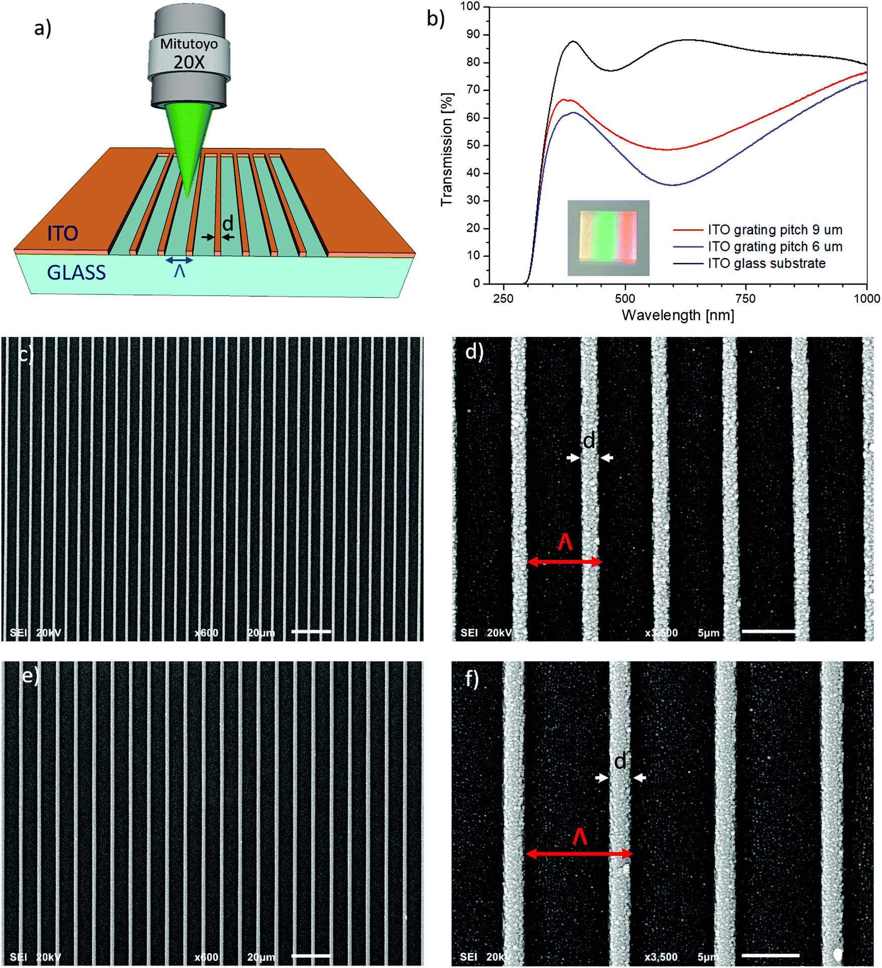 | ||
| Fig. 1 Sketch of the ITO pattern made by femtosecond-laser fabrication (a). Comparison of transmission spectra of pure ITO glass substrate, and patterned ITO areas (capture) with a pitch of 6 μm and 9 μm (b), with an image of the fabricated grating in the inset. Different scale SEM images of the two patterns fabricated, with pitch Λ = 6 μm and d = 1.5 μm (c and d) and Λ = 9 μm and d = 1.9 μm (e and f). | ||
After the ablation, the sample was cleaned in an ultrasonic bath of water and isopropanol mixed solution to remove possible remaining debris. The obtained ITO pattern was quality controlled in its dimensions using scanning electron microscopy (SEM). Different scale SEM images of the patterns are reported in Fig. 1c–f. The optical properties of the ITO, patterned or unpatterned films, have been initially investigated by measuring the transmission spectra in the range of 220 nm up to 1000 nm. Machined ITO shows a clear change in the spectral transmission in the visible spectral range compared to the pure substrate, as reported in Fig. 1b. This variation in optical signal is ascribed to the appearance of the photonic stop band of the grating due to the periodic arrangement of the structure.
For comparison, we also measured the transmission spectra in the near infrared region up to about 2200 nm (see Fig. S2 of the ESI†), which shows that the ITO film is nearly transparent in the visible range, while in the infrared part of the spectra, the presence of the plasmonic resonance decreases the transmission from 80% to below 10%. The valley at about 400 nm is due to the interband absorption of ITO. These results show clearly that the strong transmission dip around 600 nm is due to the microfabrication of the ITO patterns.
Ultrafast pump probe spectroscopy
To study the variation of the signal in our ITO gratings, we chose two different excitation schemes: pumping at 1500 nm in order to achieve intraband excitation and pumping at 266 nm to excite the interband transitions. First, we focus on the intraband excitation with an ultrashort pulse that is resonant with the plasmon resonance of the ITO and we study the reference ITO thin film without the grating structure. In Fig. 2, we show the results of our intraband ultrafast experiment performed on ITO.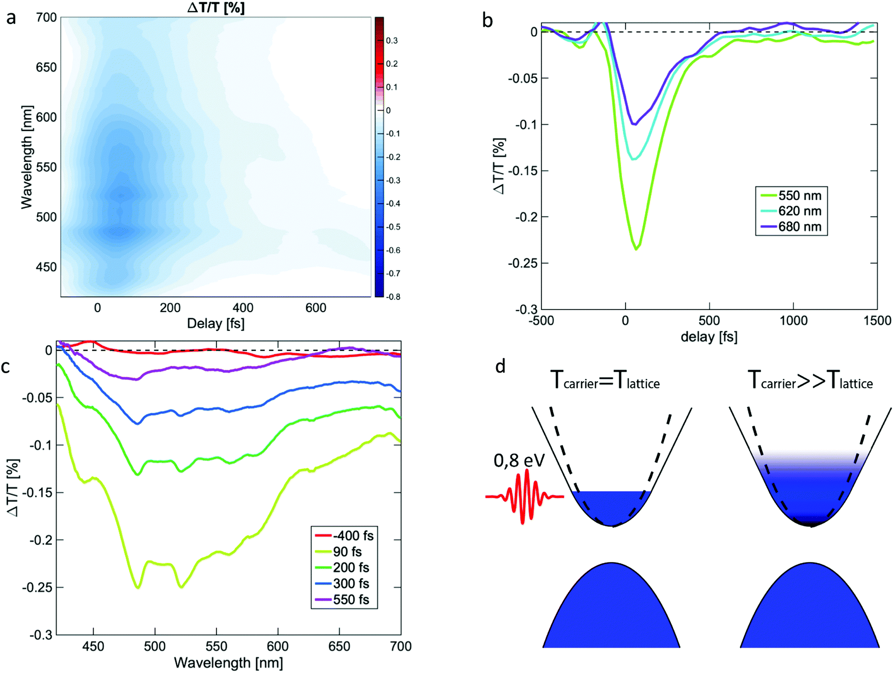 | ||
| Fig. 2 (a) Differential transmission 2D map as a function of wavelength and time delay for the ITO film; (b) temporal behavior at 500 nm; (c) spectral evolution at different time delays; (d) sketch of the intraband excitation in ITO and non-parabolicity of the ITO band. | ||
Fig. 2a shows a color coded pump probe map in the range of 450–700 nm, where we see a broad negative signal. In Fig. 2b and c, we can see two different cuts of the map: in Fig. 2b, we plot the recovery dynamics at different wavelengths and we can see that we have a sub-picosecond relaxation that is associated with electron–phonon scattering in ITO, while in Fig. 2c, we plot the evolution of the whole spectrum at some selected pump–probe delay. When exciting the electron gas of a metal with resonant light pulses, an out of equilibrium distribution of hot electrons is created. In the first tens of femtoseconds, the electrons thermalize to a hot Fermi–Dirac distribution with an electronic temperature Tcarrier ≫ Tlattice. This gives the highest transient signal in ultrafast measurements. Thereafter, the hot electron distribution cools down through electron–phonon scattering (Fig. 2d), which results in the initial ultrafast decay observed in Fig. 2c within the first picosecond of the measurement.18,19 The second longer decay then is a result of the hot lattice after the carriers cooled down.
Intraband excitation of ITO gratings
The fabrication of the ITO grating allows us a control of the ultrafast modulation of an optical signal in terms of either an increase (positive ΔT/T) or a decrease (negative ΔT/T) of light transmission through the sample. Such control is determined via the choice of the grating pitch. We show the result of the intraband excitation measurement on the two gratings in Fig. 3. In Fig. 3a, we can see that in this case, we have a positive and a negative signal in the measurement, differently than in the case of ITO film. This change of transmission arises from the shift of transmission minima of the grating caused by an ultrafast modulation of the refractive index of the ITO. The dielectric permittivity, i.e. the square of the refractive index, of materials with a significant free carrier density, such as ITO, can be described well by the Drude function. This depends on the high frequency dielectric constant ε∞ of the material and the plasma frequency ωp, which itself is a function of the carrier density and the effective mass. Since intraband pumping does not excite any additional electron from the valence band, we are not changing the carrier density. The change of refractive index instead is associated with a change in the plasma frequency arising from a variation of the effective mass of the carriers m*, due to the non-parabolicity of the conduction band of heavily doped semiconductors. In a parabolic band, the associated effective mass is constant all along the band dispersion, while in a non-parabolic one, the effective mass depends on the energy of the carriers, and m* increases with increasing energy.12 In fact, this strong modulation of the photonic bandgap in the visible spectral region as observed by us is a result of an intense variation of the dielectric permittivity as a result of the effective mass variation of the hot carriers (and not the high frequency dielectric constant ε∞ as in noble metals).12 We further observed that we can modulate the spectral window of the ultrafast variation by controlling the fabrication parameters, giving us room for the direct design of signal modulation in the visible spectral range (see Fig. S3 of the ESI†).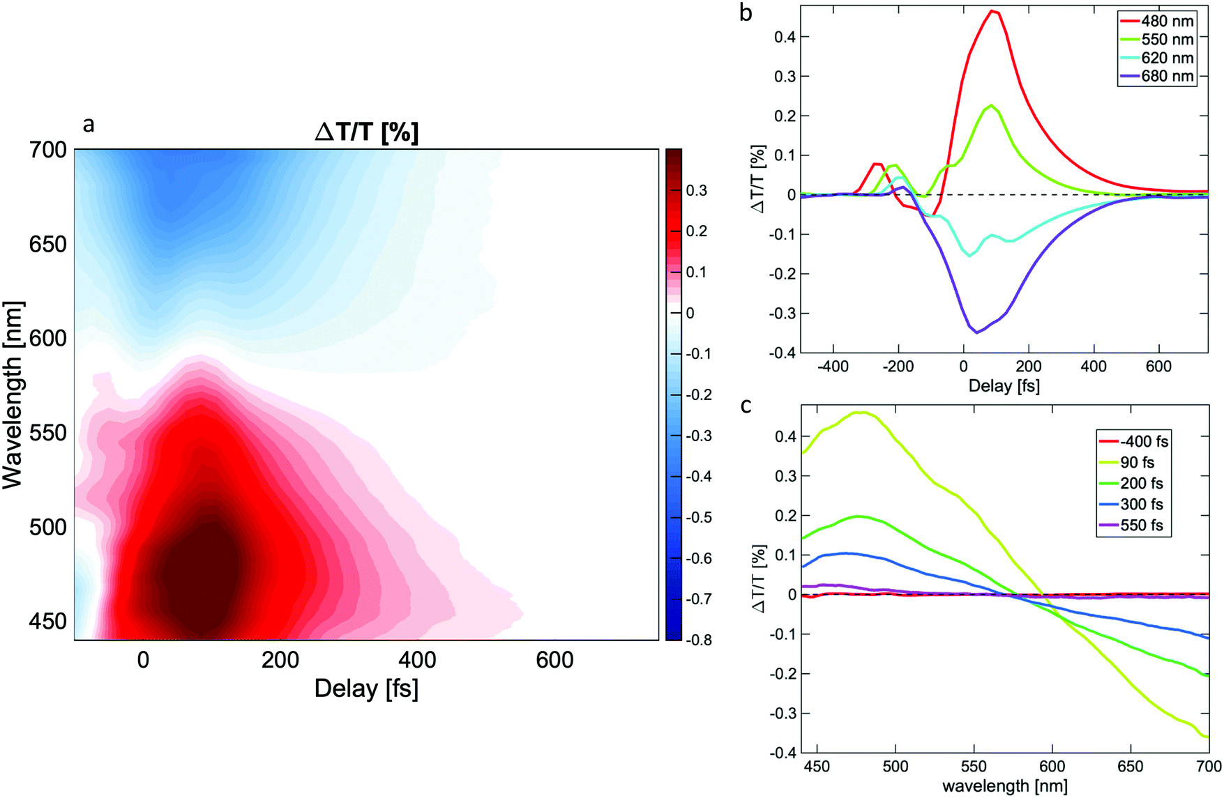 | ||
| Fig. 3 Intraband dynamics: (a) Differential transmission 2D map of the grating. (b) Recovery dynamics of the grating. (c) Spectral evolution at different time delays. | ||
The relaxation dynamics as seen in Fig. 3b is driven by the electron cooling and is sub-picosecond, resulting in a two orders of magnitude faster decay channel than in metals, e.g. gold.20 The presence of the glass behind the ITO causes the so called cross-phase modulation (XPM) artifact. This can be seen in the dynamics, where before the decay, we have some unwanted modulation. This is induced by the change of the refractive index in the glass caused by the huge amount of photons passing through.21 This does not in any case change the relaxation dynamics. The artifact does not have a proper dynamics and after the artifact ends, we have zero contribution from it.
Thus, we have shown the possibility to shift the photonic features of the ITO grating in the visible spectral region by exciting ITO in the near-infrared region, exploiting the non-parabolicity of the ITO conduction band.
Interband excitation of ITO gratings
As a final investigation, we pumped the interband transitions of ITO by using a pump pulse at 266 nm, which is beyond the bandgap of ITO. In this scenario, the energy of the photons is enough to promote an electron from the valence band to the conduction band. This results in an increase of the carrier density, which in turn increases the plasma frequency ωp and, thus, has an overall effect on the dielectric permittivity. The results for both the thin films and the gratings are shown in Fig. 4. For both cases, a negative signal is observed corresponding to a decrease of the transmission. Notably, the ITO film in Fig. 4 is governed by sub-picosecond decay, while the result from our grating appears to have a much slower decay. In the case of thin ITO film, the decay dynamics look very similar to what is observed in the intraband transition case, i.e. a two-step decay with an ultrafast component of less than 0.5 picoseconds, and a second slower one over several hundreds of picoseconds, which resembles strongly the direct excitation of the plasmon resonance. The usual process takes place: electron–electron scattering and electron phonon scattering, followed by the cooling of the lattice. This is a typical signal response of thin heavily doped metal oxide films.22 It is notable that we are able to modify the signal response of the ITO film strongly by forming the grating structure. It appears that this structural arrangement strongly confined in width on the micrometer scale favors the excitation of the interband processes. This latter signal displays a signal build-up of about 150 femtoseconds, followed by an initial decay within the first 100 picoseconds. We interpret the results in the following way: the initial rise time is a result of the cooling of the hot carriers that were excited way beyond the bandgap to the edge of the conduction band of the material. The following exponential decay resembles strongly the electron–hole recombination of semiconductors (see Fig. S4 of the ESI†).23 Thereafter, a long-living signal is observed, which we assign to either the strong heating of the lattice due to the creation of the initial hot carriers, or, more likely, to the creation of trap states induced by the femtosecond laser micro-machining process that changes the relaxation path of the electrons. Possibly, the trapping of the carriers towards the surface of the fabricated structure extends the lifetime of the carriers and therefore favors the interband relaxation processes, observed by us in the grating structure and similar to what has been observed in other confined structures of heavily doped metal oxides.23,24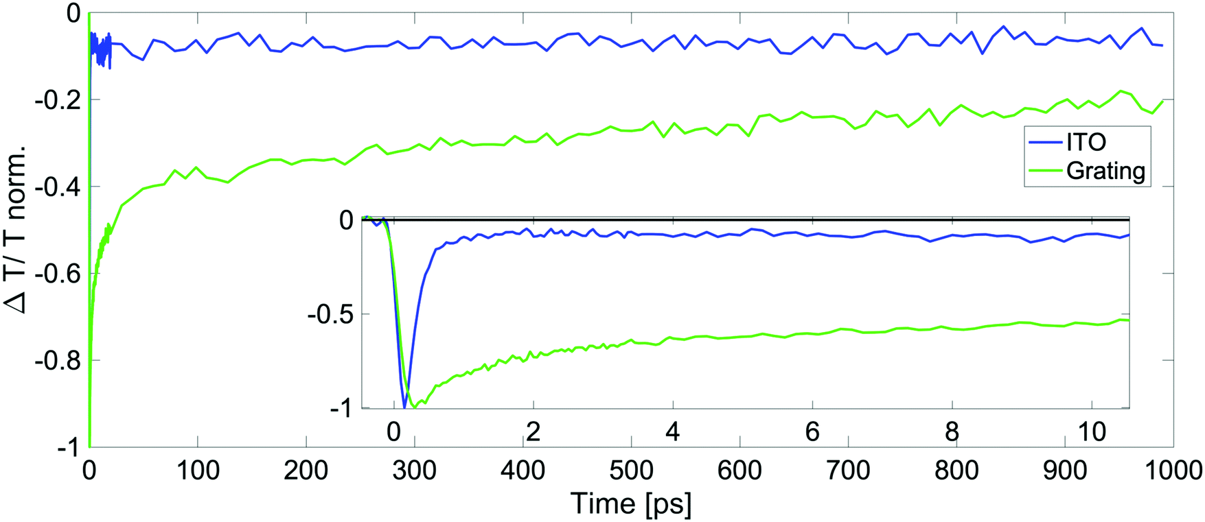 | ||
| Fig. 4 Interband dynamics and comparison of normalized decay at 550 nm between thin film and ITO grating (inset: zoom of the dynamics in the first 10 picoseconds). | ||
Thus, the interband excitation leads to a change of the dielectric permittivity of ITO and sheds light on the trap states in the ITO grating induced by the fabrication.
Conclusion
In conclusion, we demonstrate the fabrication of ITO grating structures with varying width and pitch distance via femtosecond laser micromachining. This technique allowed us to create large areas of periodic structures in the millimeter regime and therefore enabled the work with laser beams with large beam waists, reducing the use of optical components. Our transient absorption measurements display an ultrafast signal modulation on the picosecond time scale. A further investigation would be the refinement of a theoretical tool that takes into account how the transmittivity of the grating is changed after the pump pulse is absorbed, and this can be quantified by modeling the temporal behavior of the dielectric permittivity of ITO in the case of interband and intraband excitation. Such modelized dielectric permittivity can be employed to understand the temporal behavior of the ITO gratings. The formation of the grating structure delivers the opportunity to control exactly the signal wavelength and to induce transmission suppression and enhancement in the visible spectral range as a result of the refractive index variation of ITO on the ultrafast timescale. Such control could be exploited for all-optical signal modulation, which has been demonstrated by employing ITO nanorods13 and in nanoantenna-ITO hybrids.25 We suggest here a modulation that is similar to the one suggested by Guo et al.:13 we use near infrared laser pulses of about 100 fs to modulate the transmission spectrum of the ITO grating in the visible spectral region exploiting the modulation of the dielectric permittivity of ITO. Our results show that picosecond spectral modulation in the visible spectral region becomes accessible in ITO microarray structures on a scale of 5 × 5 mm fabricated by femtosecond laser micromachining, bringing this system closer to industrial relevance.Conflicts of interest
There are no conflicts to declare.Acknowledgements
This project has received funding from the European Research Council (ERC) under the European Union's Horizon 2020 research and innovation programme (grant agreement No. [816313]). Moreover, this project has received funding from the European Union's Horizon 2020 research and innovation programme (SONAR) under the Marie Skłodowska-Curie grant agreement no. [734690].References
- I. Kriegel, F. Scotognella and L. Manna, Plasmonic doped semiconductor nanocrystals: properties, fabrication, applications and perspectives, Phys. Rep., 2017, 674, 1–52 CrossRef CAS.
- A. Agrawal, R. W. Johns and D. J. Milliron, Control of Localized Surface Plasmon Resonances in Metal Oxide Nanocrystals, Annu. Rev. Mater. Res., 2017, 47, 1–31 CrossRef CAS.
- A. Comin and L. Manna, New materials for tunable plasmonic colloidal nanocrystals, Chem. Soc. Rev., 2014, 43, 3957–3975 RSC.
- F. Scotognella, G. Della Valle, A. R. Srimath Kandada, M. Zavelani-Rossi, S. Longhi, G. Lanzani and F. Tassone, Plasmonics in heavily-doped semiconductor nanocrystals, Eur. Phys. J. B, 2013, 86, 154, DOI:10.1140/epjb/e2013-40039-x.
- A. L. Routzahn, S. L. White, L.-K. Fong and P. K. Jain, Plasmonics with Doped Quantum Dots, Isr. J. Chem., 2012, 52, 983–991 CrossRef CAS.
- J. M. Luther, P. K. Jain, T. Ewers and A. P. Alivisatos, Localized surface plasmon resonances arising from free carriers in doped quantum dots, Nat. Mater., 2011, 10, 361–366 CrossRef CAS PubMed.
- P. P. Edwards, A. Porch, M. O. Jones, D. V. Morgan and R. M. Perks, Basic materials physics of transparent conducting oxides, Dalton Trans., 2004, 2995–3002 RSC.
- N. R. Armstrong, P. A. Veneman, E. Ratcliff, D. Placencia and M. Brumbach, Oxide Contacts in Organic Photovoltaics: Characterization and Control of Near-Surface Composition in Indium−Tin Oxide (ITO) Electrodes, Acc. Chem. Res., 2009, 42, 1748–1757 CrossRef CAS PubMed.
- M. Z. Alam, I. D. Leon and R. W. Boyd, Large optical nonlinearity of indium tin oxide in its epsilon-near-zero region, Science, 2016, 352, 795–797 CrossRef CAS PubMed.
- S.-Q. Li, P. Guo, D. B. Buchholz, W. Zhou, Y. Hua, T. W. Odom, J. B. Ketterson, L. E. Ocola, K. Sakoda and R. P. H. Chang, Plasmonic–Photonic Mode Coupling in Indium-Tin-Oxide Nanorod Arrays, ACS Photonics, 2014, 1, 163–172 CrossRef CAS.
- D. B. Tice, S.-Q. Li, M. Tagliazucchi, D. B. Buchholz, E. A. Weiss and R. P. H. Chang, Ultrafast Modulation of the Plasma Frequency of Vertically Aligned Indium Tin Oxide Rods, Nano Lett., 2014, 14, 1120–1126 CrossRef CAS PubMed.
- P. Guo, R. D. Schaller, J. B. Ketterson and R. P. H. Chang, Ultrafast switching of tunable infrared plasmons in indium tin oxide nanorod arrays with large absolute amplitude, Nat. Photonics, 2016, 10, 267–273 CrossRef CAS.
- P. Guo, R. D. Schaller, L. E. Ocola, B. T. Diroll, J. B. Ketterson and R. P. H. Chang, Large optical nonlinearity of ITO nanorods for sub-picosecond all-optical modulation of the full-visible spectrum, Nat. Commun., 2016, 7, 12892 CrossRef CAS PubMed.
- P. Guo, R. P. H. Chang and R. D. Schaller, Transient Negative Optical Nonlinearity of Indium Oxide Nanorod Arrays in the Full-Visible Range, ACS Photonics, 2017, 4, 1494–1500 CrossRef CAS.
- G. M. Paternò, C. Iseppon, A. D’Altri, C. Fasanotti, G. Merati, M. Randi, A. Desii, E. A. A. Pogna, D. Viola, G. Cerullo, F. Scotognella and I. Kriegel, Solution processable and optically switchable 1D photonic structures, arXiv:1711.03192 [cond-mat, physics:physics].
- S. L. Turco, A. D. Donato and L. Criante, Scattering effects of glass-embedded microstructures by roughness controlled fs-laser micromachining, J. Micromech. Microeng., 2017, 27, 065007 CrossRef.
- G. Cerullo, C. Manzoni, L. Lüer and D. Polli, Time-resolved methods in biophysics. 4. Broadband pump–probe spectroscopy system with sub-20 fs temporal resolution for the study of energy transfer processes in photosynthesis, Photochem. Photobiol. Sci., 2007, 6, 135–144 RSC.
- G. V. Hartland, Optical Studies of Dynamics in Noble Metal Nanostructures, Chem. Rev., 2011, 111, 3858–3887 CrossRef CAS PubMed.
- F. Scotognella, G. Della Valle, A. R. Srimath Kandada, D. Dorfs, M. Zavelani-Rossi, M. Conforti, K. Miszta, A. Comin, K. Korobchevskaya, G. Lanzani, L. Manna and F. Tassone, Plasmon Dynamics in Colloidal Cu2−x Se Nanocrystals, Nano Lett., 2011, 11, 4711–4717 CrossRef CAS PubMed.
- S. Link and M. A. El-Sayed, Spectral Properties and Relaxation Dynamics of Surface Plasmon Electronic Oscillations in Gold and Silver Nanodots and Nanorods, J. Phys. Chem. B, 1999, 103, 8410–8426 CrossRef CAS.
- M. Lorenc, M. Ziolek, R. Naskrecki, J. Karolczak, J. Kubicki and A. Maciejewski, Artifacts in femtosecond transient absorption spectroscopy, Appl. Phys. B: Lasers Opt., 2002, 74, 19–27 CrossRef CAS.
- N. Kinsey, C. DeVault, J. Kim, M. Ferrera, V. M. Shalaev and A. Boltasseva, Epsilon-near-zero Al-doped ZnO for ultrafast switching at telecom wavelengths, Optica, 2015, 2, 616–622 CrossRef CAS.
- I. Kriegel, C. Urso, D. Viola, L. De Trizio, F. Scotognella, G. Cerullo and L. Manna, Ultrafast Photodoping and Plasmon Dynamics in Fluorine–Indium Codoped Cadmium Oxide Nanocrystals for All-Optical Signal Manipulation at Optical Communication Wavelengths, J. Phys. Chem. Lett., 2016, 7, 3873–3881 CrossRef CAS PubMed.
- B. T. Diroll, P. Guo, R. P. H. Chang and R. D. Schaller, Large Transient Optical Modulation of Epsilon-Near-Zero Colloidal Nanocrystals, ACS Nano, 2016, 10, 10099–10105 CrossRef CAS PubMed.
- M. Abb, P. Albella, J. Aizpurua and O. L. Muskens, All-Optical Control of a Single Plasmonic Nanoantenna-ITO Hybrid, Nano Lett., 2011, 11, 2457–2463 CrossRef CAS PubMed.
Footnote |
| † Electronic supplementary information (ESI) available. See DOI: 10.1039/c9cp06839b |
| This journal is © the Owner Societies 2020 |