Van der Waals induced molecular recognition of canonical DNA nucleobases on a 2D GaS monolayer
Received
27th November 2019
, Accepted 25th February 2020
First published on 25th February 2020
Abstract
In the present study, we systematically investigated the adsorption mechanism of canonical DNA nucleobases and their two nucleobase pairs on a single-layer gallium sulfide (GaS) substrate using DFT+D3 methods. The GaS substrate has chemical interactions with molecules 0.02 |e| 0.11 |e| from molecules to the monolayer GaS surface. Due to the chemical interactions of adenine, cytosine, guanine, and thymine on the monolayer GaS surface, the work function is decreased by 0.69, 0.60, 0.97, and 0.20 eV, respectively. It is displayed that the bandgap of the monolayer GaS sheet can be significantly affected as induced molecular electronic states tend to appear near the Fermi level region due to chemical and physisorption mechanism. We have also investigated the transport properties of DNA nucleobases, namely, AT and GC pair molecules on the GaS surface, which shows significant reduction in the zero-bias transmission spectra. Moreover, with and without DNA nucleobases, namely, AT and GC pair molecules’ absorptions on the GaS surface, clearly expressed in terms of distinct current signals, can be observed as ON and OFF states for this device. The distinctive nucleobase adsorption energies and different I–V responses may serve as potential probes for the selective detection of nucleobase molecules in imminent DNA sequencing applications based on a monolayer GaS surface.
Introduction
Molecular recognition and self-assembly process of DNA with 2D materials have reinvigorated strategies for personalized medicine and biomedical applications using the elimination of dependence on the biological regime for which it is contemplated or conceived as a possible, desirable future event for many researchers.1 To a greater extent, theoretical studies have been proposed in many 2D materials for the physisorption of nucleobases. However, the major challenge lies in the sensitivity and specificity of nucleobase detection. Layered semiconductors that have been extensively studied due to their peculiar electronic properties and a promising class of 2D topological insulators include Group-III monochalcogenides (MX, M = Ga, In; X = S). The functionalization of 2D materials is an effective strategy for tailoring the properties to trigger several phenomena such as physisorption, chemisorption, and many biological regimes. Physical adsorption of nucleobases has not been investigated previously using the GaS monolayer. The results of our first-principles study on the interaction of nucleobases with a GaS monolayer surface may serve as a viewpoint for understanding the interaction of ssDNA with the GaS monolayer.
GaS monolayer has been studied in previous literature,2,3 which possesses a carrier mobility of 0.6 cm2 V−1 s−1,4 tunable electronic properties via external electric fields and strains,2,5 exciting anisotropic features, controllable optical properties,6 and better photocatalyst for water splitting.7 Meanwhile, a stable class of 2D metal dichalcogenides (MD) materials, GaS monolayer has been synthesized experimentally,4,8 opening an attractive type of materials for optoelectronic applications. These fascinating characteristics make monolayer GaS promising for applications in high-performance photodetectors on both the conventional silicon and flexible substrates3 as an efficient candidate for making single-sheet based field-effect transistors (FET).4 Additionally, a photodetector based on few-layer GaS was established to show the disparities in photoresponsivity in different gas environments. A higher photoresponsivity and external quantum efficiency was obtained in ammonia than in air or oxygen.9
Motivated by the promising achievements of monolayer GaS, we have explored the adsorption of DNA nucleobase molecules on the surface of GaS monolayer using DFT calculations. Superior interactive configurations of these nucleobase molecules were obtained by computing the adsorption energies. The charge transfer mechanism between the adsorbed nucleobase molecules and the monolayer GaS surface was then theoretically calculated to determine the doping behaviour of these nucleobase adsorbates. The monolayer GaS structures also regulate the work function of GaS and adsorbates of the nucleobase molecule complexes. Our present findings highlight the significance of monolayer GaS in dominating the electronic properties of GaS and adsorbates of nucleobase molecule complexes; this would also be important to guide the design and fabrication of strategies for the detection of nucleobase molecules in future DNA sequencing devices.
Theoretical methods
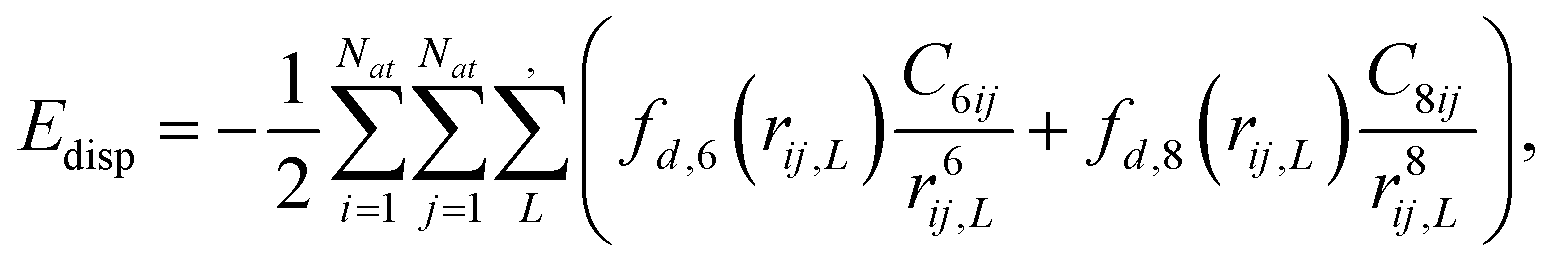
Density functional theory (DFT) based calculations using the generalized gradient approximation (GGA) with Perdew–Burke–Ernzerhof (PBE) exchange functional,10–12 as implemented in the Vienna Ab initio Simulation Package (VASP) software,12–14 were performed. It is a well-known fact that GGA-PBE underestimates the binding energies coupled with the van der Waals forces that influence the binding properties. With a hindsight on the underestimation of the van der Waals correction, we employed the DFT-D3 method15 of Grimme, as implemented in the VASP software. The DFT-D3 method determines the self-consistent total energy obtained from Kohn–Sham DFT (KS-DFT) additionally corrected by the Edisp term, as given by:| | | EDFT-D3 = EKS-DFT + Edisp | (1) |
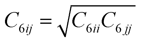
where the underlying Edisp is a pairwise term accounting for the long-range van der Waals (vdW) interactions and is defined as,| | 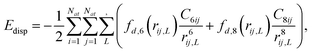 | (2) |
Here,  , is the dispersion coefficient,
  is the vdW radius, and f(rij)is the damping function.
We have used 6 × 6 × 1 supercell of GaS monolayer having 144 atoms (72 Ge and 72 S atoms). The energy cutoff of 500 eV was employed and a vacuum space of about 24 Å was used in the z-direction to minimize physical interactions between consecutive sheets. The Brillouin Zone (BZ) was validated with 3 × 3 × 1 k-points by using the Monkhorst–pack scheme16 along with the energy and force convergence of 10−6 eV and 0.001 eV Å−1, respectively. Bader charge analysis17 was performed to depict the charge transfer between the GaS monolayer and the molecules. The absorption energy was deduced using the following relation between the DNA nucleobases and aromatic amino acids with the GaS monolayer:
| | | Eabs = Esheet+molecule − Esheet − Emolecule, | (3) |
where,
Esheet+molecule,
Esheet, and
Emolecule represent the total energy of the sheet with the molecule, pristine sheet, and molecule, respectively. In general, the energetically favorable reaction represents an exothermic reaction followed by negative values, while the endothermic reaction gives positive values that represent energetically unfavorable reactions. The charge transfer between the GaS surface and the molecules was calculated by Bader charge analysis. During the Bader charge calculations, we have used the full all-electron charge density, which calculates the fine FFT-grid.
In order to further investigate the potential of the GaS monolayer for the adsorption of DNA nucleobase pairs AT and GC, the electronic transport properties of the GaS monolayer prior to and post DNA nucleobase pairs AT and GC adsorption was carried out using the non-equilibrium Green's function (NEGF) in TranSiesta module of Siesta code.18,19 For this purpose, we again systematically relaxed the GaS monolayer with the DNA nucleobase pairs AT and GC systems in Siesta with an energy cutoff of 350 Ry using double-polarized (DZP) basis sets. For Siesta calculations, however, we also considered the van der Waals interactions (Grimme). For the geometry, optimization was achieved when the maximum difference between the output and input on each element of the Density Matrix was less than 10−4. The electron wave function was expanded using a DZP basis set. Monkhorst–Pack k-point grids of 10 × 1 × 100 and 10 × 1 × 1 were employed for electrode and transport calculations, respectively. The electric current through the atomic scale system was calculated from the Landauer–Buttiker formula;
| |  | (4) |
where,
T(
E,
Vb) is the transmission coefficient at energy
E and applied bias voltage
Vb, and it is followed by
T(
E,
Vb) = Tr[
ΓR(
E,
Vb)
GR(
E,
Vb)
ΓL(
E,
Vb)
GA(
E,
Vb)] quantity, which is the probability that an incoming electron with energy
E at a given bias
Vb will be transmitted across the scattering region. Also,
μL and
μR are the two electrochemical potentials of left and right electrodes, respectively,
f(
E) is the Fermi–Dirac distribution function, and
G0 = 2
e2/
h is the quantum conductance. As seen from the above equation, the current is the integral of the transmission coefficient over the applied bias window.
Results and discussion
Structural and electronic properties
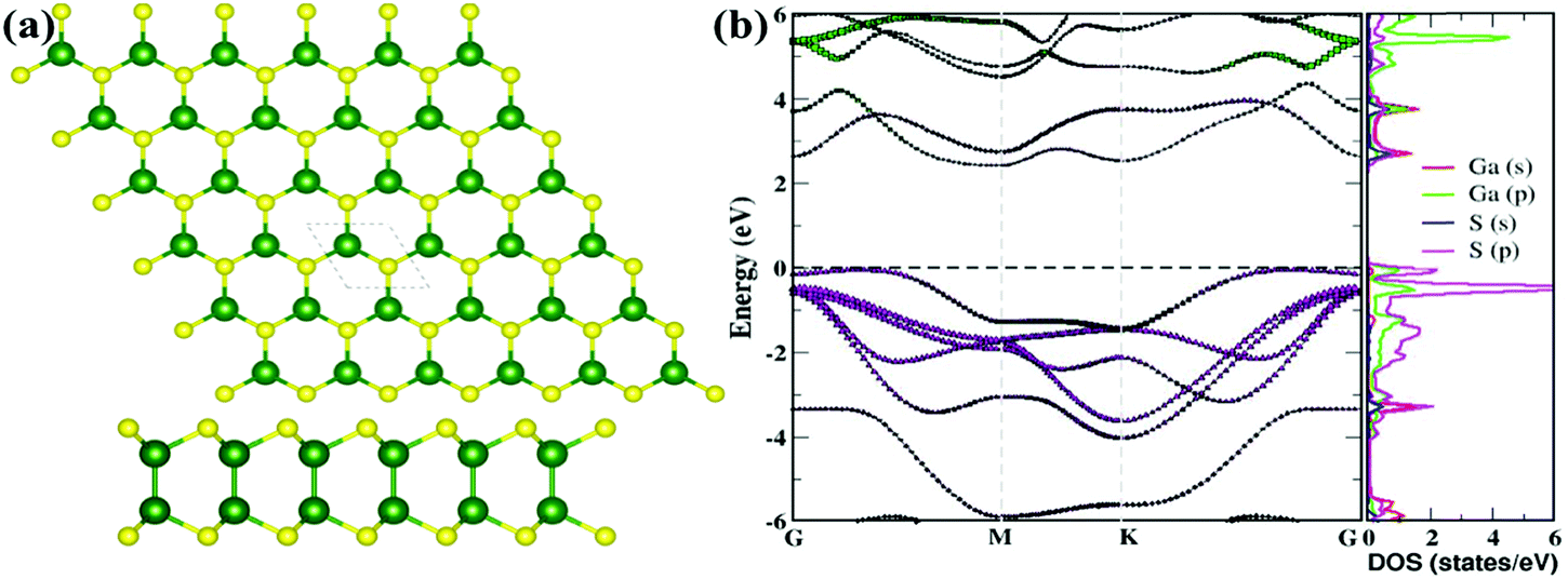
The computed lattice parameters of pristine gallium sulfide (GaS) monolayer are 3.58 Å, bond lengths of Ga–Ga and Ga–S are 2.47 Å and 2.35 Å, respectively (see Fig. 1(a)), which are well consistent with the previously reported theoretical as well as experimental works.3,7,8 The thickness of the GaS layer is 4.71 Å. The computed net electronic charges are +0.84 |e|and −0.84 |e| for Ga and S atoms, respectively, based on Bader analysis.17 The electronic band structures and projected density of states are depicted in Fig. 1(b). Analyzing the band structure, pristine GaS is noticeably a semiconductor with an indirect bandgap of 2.50 eV, while a direct bandgap was also observed (2.79 eV). Along with the band structures, the projected density of states was illustrated to understand the orbital contribution to the valence band maximum (VBM) and conduction band minimum (CBM). The top of VBM in the band structure is mainly contributed by p-orbitals of S atom and has a weak component from p-orbitals of Ga atom. On the other hand, the bottom of CBM is made by s-orbital of Ga atom and P-orbital of S atom, as presented in Fig. 1(b), which is consistent with the previous work. Conduction bands are primarily made of s- and p-orbitals of Ga.7
 |
| | Fig. 1 (a) The optimized structure, (b) corresponding band structure and projected density of states (PDOS) of the pristine GaS sheet. | |
Furthermore, we have taken 6 × 6 × 1 supercell of GaS monolayer having 144 atoms (72 Ge and 72 S atoms) in a single unit cell for the absorption mechanism of nucleobases. During the geometry relaxation process, each nucleobase molecule is placed at 3.0 Å vertical distance from the top layer of the S-atoms in the monolayer GaS. We took two possible orientations of the nucleobase; one is parallel to the sheet and the other is vertical to the sheet. The most energetically favorable optimized structures have been depicted in Fig. 2 and 3. It is noticed that the nucleobase A favorably adopts a parallel orientation whereas C, G, T, and their pairs A–T and G–C are slightly tilted towards the GaS sheet. Due to the high electronegativity of oxygen atom, DNA molecules (oxygen-containing molecules) tend to interact more with the GaS sheet, which is oriented/tilted towards the GaS surface. Due to the absence of oxygen atoms in A nucleobase, it is oriented parallel to the GaS sheet, as presented in Fig. 2. The computed vertical height between the nucleobase molecules A, C, G, T, and their pairs A–T and G–C with the monolayer GaS surface are about 3.24, 3.19, 2.48, 2.65, 2.68, and 2.91 Å, and the corresponding absorption energies are predicted to be −0.49, −0.44, −0.71, −0.63, −2.02, and −2.49 eV, respectively. The absorption energy of nucleobase pair A–T and G–C is higher than that of the individual nucleobases. The adsorption energy of G and T is higher than that of A and C due to the strong affinity of oxygen atoms with the GaS sheet. The order of absorption energies of A, C, G, and T on the surface of GaS is G > T > A > C, which is different from graphene, MoS2 and WS2 monolayer (G > A > T > C), antimonene (G > A > C > T), silicene (G > A > T > C), and germanene (G > A > T > C), as calculated by van der Waals (vdW) corrected DFT method.20–22 The absorption energy illustrated in our work was noted to be in the order GC > AT in accordance with the absorption energy, while the previously reported work on antimonene for nucleobase pair show sAT > GC.20 From the above results as well as the previously reported works, we concluded that G energetically interacts with the surface. We have also reported the charge transfer mechanism using Bader charge analysis and we found that A, C, G, and T gain 0.05, 0.05, 0.06, and 0.04 e from the GaS sheet, respectively. In addition, nucleobase pairs AT and GC gain more charges, viz., 0.11 and 1.10 e, from the monolayer GaS sheet. Moreover, we also investigated the binding strength of the vertical nucleobase concerning the GaS sheet. The absorption energies of −0.18, −0.17, −0.33, and −0.52 eV for each nucleobase A, C, G, and T, respectively, were observed during the vertical alignments with the GaS monolayer, while the nucleobase pairs AT and GC give −1.47 and −1.91 eV, respectively. The calculated vertical height of these nucleobases A, C, G, and T, and the pairs AT and GC were about 2.17, 2.18, 2.06, 2.21, 2.21, and 2.11 Å, respectively, which is lower than the parallel orientations of the nucleobases displayed above. According to charge analysis, the results showed A, C, G, T, AT, and GC gains of 0.04, 0.02, 0.03, 0.03, 0.07, and 0.07 e from the GaS surface, respectively. From these findings, it can be depicted that the nucleobase pairs AT and CG have more binding energy and gain more charge as compared to single nucleobases on the monolayer GaS sheet (see Table 1).
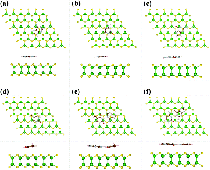 |
| | Fig. 2 Fully optimized structures of DNA nucleobases, aromatic amino acids on the surface of the GaS monolayer. (a) Adenine, (b) cytosine, (c) guanine, (d) thymine, (e) base pair adenine–thymine, and (f) cytosine–guanine horizontally absorbed on the GaS surface. | |
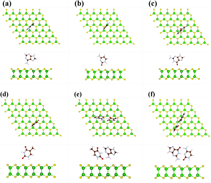 |
| | Fig. 3 Fully optimized structures of DNA nucleobases, aromatic amino acids on the surface of the GaS monolayer. (a) Adenine, (b) cytosine, (c) guanine, (d) thymine, (e) base pair adenine–thymine, and (f) cytosine–guanine vertically absorbed on the GaS surface. | |
Table 1 Structural parameters of DNA nucleobases, aromatic amino acids on the surface of GaS monolayers such as horizontal and vertical heights (Å) of GaS monolayer and molecules, adsorption energies (eV), charge transfer (e) from the GaS surface to the molecules, work function, Φ (eV) and changes of work function, ΔΦ (eV) with the interaction of molecules on the surface of GaS monolayer
| System |
A |
C |
G |
T |
A–T |
G–C |
| Heights, H/V |
3.24/2.17 |
3.19/2.18 |
2.48/2.06 |
2.65/2.21 |
2.68/2.21 |
2.91/2.11 |
|
E
a
|
−0.49/−0.18 |
−0.44/−0.17 |
−0.71/−0.33 |
−0.63/−0.52 |
−2.02/−1.47 |
−2.49/−1.91 |
| Charge transfer |
0.05/0.03 |
0.05/0.02 |
0.06/0.03 |
0.04/0.03 |
0.11/0.07 |
1.10/0.07 |
|
Φ (eV) |
5.56/5.30 |
5.64/5.52 |
5.28/5.21 |
6.04/5.91 |
5.42/5.13 |
4.86/4.32 |
| ΔΦ (eV) |
0.69/0.94 |
0.60/0.72 |
0.97/1.03 |
0.20/0.34 |
0.83/1.12 |
1.38/1.93 |
Electronic properties of monolayer GaS with the interaction of nucleobase
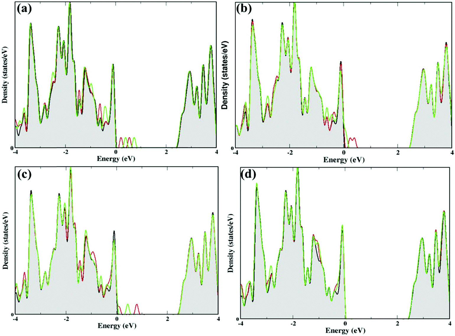
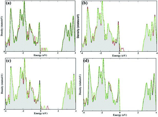
In addition, we have calculated the density of states (DOS) to understand the effect of these nucleobase molecules on the monolayer GaS surface. Fig. 4 and 5 show the DOS for nucleobase molecules A, C, G, T, AT, and GC. The absorption of A with parallel, as well as vertical orientation on the GaS sheet gives rise to significant changes in the electronic states in the DOS spectrum, as presented in Fig. 4a. For comparison, we obtained the DOS spectrum of pristine monolayer and with absorption of nucleobase molecules, as presented with black color for pristine GaS, and red and green color for parallel and vertical orientation to the GaS sheet, respectively. Near the Fermi level, the parallel orientation of nucleobase molecule A significantly reduces the bandgap of the GaS monolayer as compared to the vertical orientation of A molecule.
 |
| | Fig. 4 The density of states of pristine GaS and absorption of amino-acid on the surface of GaS. Black color represents pristine surface, and red and green color represents (a) adenine, (b) cytosine, (c) guanine, (d) thymine absorbed on the GaS surface horizontally and vertically, respectively. The zero of energy on the x-axis has been set to the Fermi energy. | |
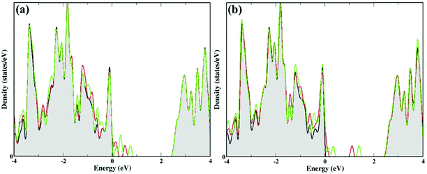 |
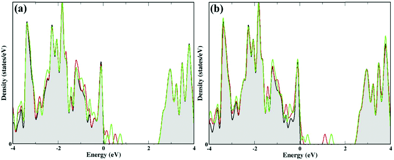
| | Fig. 5 The density of states of pristine GaS and absorption of amino-acid on the surface of the GaS surface. Black color represents the pristine monolayer, and red and green color represents the base pair (a) adenine–thymine and (b) cytosine–guanine absorbed on the GaS surface horizontally and vertically, respectively. The zero of energy on the x-axis has been set to the Fermi energy. | |
From the DOS spectrum, the primary influence was noticed in the range of −1.6 eV to −0.30 eV near the Fermi level in the occupied orbital (valence band). On the other hand, peaks are seen in the range of 0.20 eV to 0.90 eV near the Fermi level in the conduction band minimum (CBM) due to the absorption of nucleobase adenine molecule on the surface of the GaS monolayer. Further, the interactions of cytosine and guanine on the surface of the GaS monolayer are strongly influenced near the Fermi level from −0.90/−2.0 eV (valence band) to 0.50/0.90 eV (conduction band), respectively. On the other hand, the interaction of thymine with the GaS monolayer is not affected by the electronic states on the GaS monolayer near the Fermi level but from the DOS spectrum, the peak maximum is noticed in the range −1.30 eV to −0.20 eV in the valence band but is evident in the conduction band region on the right of the Fermi level. In the case of nucleobase pairs AT and GC, interactions of the GaS monolayer significantly change the electronic states, as shown in Fig. 5(a and b). Herein, nucleobase AT molecular states appeared close to the Fermi level on the valence band and conduction band between −2 eV and 1 eV, while in the case of nucleobase pairs, GC molecular states appeared between −1.50 eV to 1.50 eV from the valence band to the conduction band near the Fermi level. From the electronic properties, the monolayer GaS sheet can pay a vital role in distinguishing different nucleobase molecules in DNA sequencing.
Charge distributions and work function
To check the interaction mechanism between the nucleobases and the monolayer GaS surface, we computed the charge density redistribution (Δρ) plot, which is as follows:| | | ρ = ρGaS+nucleobase − ρGaS − ρnucleobase, | (5) |
where, ρGaS+nucleobase, ρGaS, and ρnucleobase are the total charge density of the nucleobase molecules on the GaS monolayer, isolated pristine GaS monolayer, and isolated nucleobase molecule. The charge density difference redistribution profiles of the adsorbed nucleobase molecules to investigate the interactions and bonding nature are presented in Fig. 6 and 7 for the parallel and vertical orientation of each of the nucleobase molecules on the surface of the GaS monolayer. The red and blue colour charge-density iso-surfaces denote the charge accumulation and depletion regions, respectively. In all the cases, the adsorbed nucleobase molecules gain some electrons from the GaS surfaces and accumulate the isosurface around the nucleobase molecules. Due to significant charge transfer between the GaS surface and the adsorbed nucleobase molecules, a local dipole along the perpendicular direction of the surface is developed. Also, a larger charge density difference will occur due to the adsorbed nucleobase molecules, which indicates larger dipole moment between the GaS surface and the nucleobase molecules. The top of the GaS surface contains S (2.58) atom that have lower electronegativity as compared to the O (3.44) atom presented in the nucleobase molecules; this is why nucleobase molecules capture some electrons from the GaS surface. It seems that the monolayer GaS sheet involves charge rearrangement at the interface, which gives rise to an interfacial dipole, thereby causing a shift in the work function.
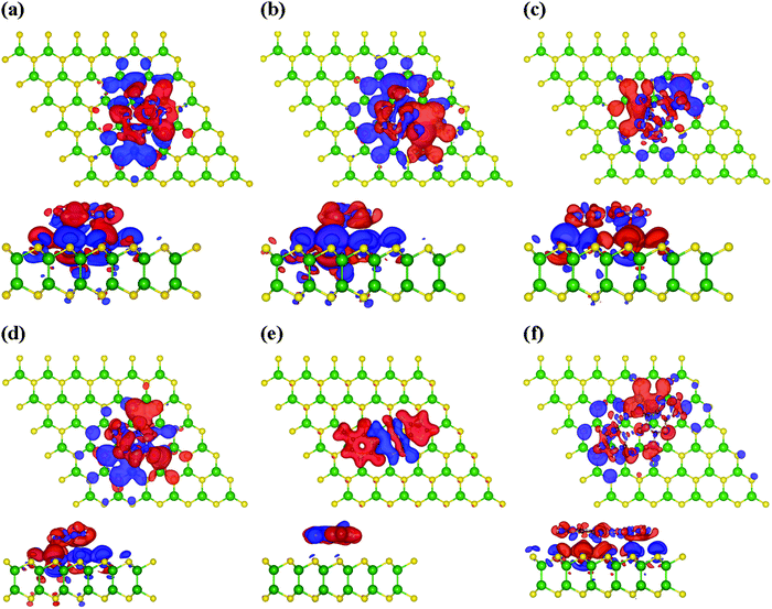 |
| | Fig. 6 Top and side views of the charge-density difference on the adsorption of nucleobase (a) A, (b) C, (c) G, (d) T, (e) AT, and (f) GC molecules in the parallel orientation on the surface of the GaS monolayer. The red and blue charge-density iso-surfaces denote the charge accumulation and depletion regions, respectively. | |
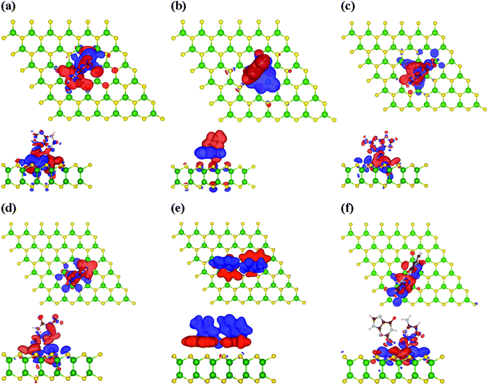 |
| | Fig. 7 Top and side views of the charge-density difference on the adsorption of nucleobase (a) A, (b) C, (c) G, (d) T, (e) AT, and (f) GC molecules in the vertical orientation on the surface of the GaS monolayer. The red and blue charge-density iso-surfaces denote the charge accumulation and depletion regions, respectively. | |
Moreover, the surface sensitivity of two-dimensional materials is a noteworthy parameter dependent on the surface potential, which could be approximated by calculating the deviation in the work function (ϕ). The energy required in separating an electron from a 2D surface to infinity (∞) is expressed by quantity ϕ. Correspondingly, the conductivity of the 2D surface is directly related to the change in ϕ, which is computed as the energy difference between the Fermi energy (EF) and the vacuum potential (Evac),
where the self-consistently governs the Fermi energy in a ground state electronic structure calculation of the system and the vacuum potential is assessed by the limiting value of the electrostatic potential in the perpendicular direction to the monolayer surface at a distance far away, which is mostly 10 Å. In our case, we have taken 24 Å to prevent physical interaction between the periodic images.
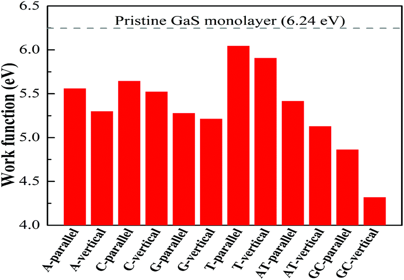
The work function of the pristine GaS monolayer is 6.24 eV, which is consistent with that in the previously reported work.7 The calculated work function for these shifts is presented in Table 1. Clearly, upon the absorption of nucleobase molecules in the single and paired form on the monolayer GaS surface, the work function is either decreased or left almost intact.23 From the obtained results, the magnitude of work function shifts for the nucleobase molecules on the GaS monolayer in the order G > A > C > T for both parallel and vertical orientations of the nucleobase, which is similar to that in the previously reported work on graphene and a single layer of MoS2 (G > A > C > T).23,24 Additionally, the nucleobase pairs AT and GC have shifts in the work function in the order GC > AT (see Table 1). These nucleobases’ single and paired molecule particular work function Φ shifts signatures, which are in the range of 0.20 eV to 1.03 eV for single nucleobase and 0.83 eV to 1.93 eV for nucleobase pairs that have likely consequences in nucleobase identifications (Fig. 8).
 |
| | Fig. 8 The significant changes in the work function with two orientations of the DNA nucleobase molecules. The dotted line in the bar plot shows the work function of the pristine GaS monolayer presented at 6.24 eV. | |
Transport properties
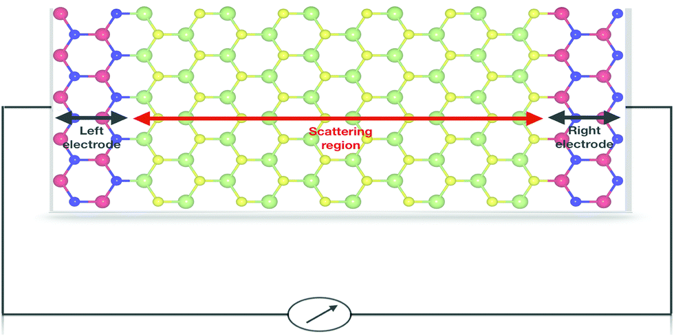
Furthermore, to evaluate the performance of the GaS monolayer for the DNA nucleobase sensing properties, we applied the NEGF approach for computing the transport properties (transmission spectra and current–voltage I–V relations) of pristine GaS monolayer and after the DNA nucleobases’ adsorption on the GaS monolayer, which allows to invigilate the change in resistivity. Herein, we have calculated the variations in current in a series of voltage with the interval of 0.5 V for GaS sheet junctions without and with adsorption of different gas molecules. The acquired results can be directly compared to experimental measurements. For the demonstrative model of transport properties, we have chosen DNA nucleobase pairs AT and GC molecules’ adsorptions on the GaS surface. In the case of transport properties presented in Fig. 9, the arrangement of the two probe systems is used, where the shaded areas represent that left and right electrodes are in contact with the central scattering region.
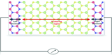 |
| | Fig. 9 Schematic illustration of the proposed device setup with left and right GaS electrodes, and a central scattering region containing the same material, the target nucleobase pairs AT and GC molecules, and a portion of the semi-infinite GaS electrodes. The blue (S atom) and red (Ga atom) atoms on both side in the device modelling represents the size of the left/right electrode. The light green and yellow color atoms represent the scattering region. | |
To better understand the effect of DNA nucleobase pairs AT and GC molecules on the GaS monolayer, we initially computed the zero-bias transmission spectra without and with the adsorption of DNA nucleobase pairs AT and GC. Fig. 10 shows the transmission spectra of without and with different gas adsorptions on the GaS monolayer at zero-bias. From Fig. 10, the zero-bias transmission spectra show a remarkable effect on the adsorption of DNA nucleobase pairs AT and GC. The adsorption of DNA nucleobase pairs AT and GC molecules shows suppressed transmission spectra, which can be credited to backscattering that reduces the available conduction channels. Similar results are found for 2D phosphorene with the absorption of different gas molecules, which shows decreased transmission.25 It seems that there is a region of zero-bias transmission near and beyond the Fermi level; there is a step-like feature in the transmission spectra, which is originated from the available conductance channels of various energy bands. It is clear that the AT molecule induces a small effect in the transmission spectra while GC has a significant effect in the transmission spectra. The reduced conductance channels reflect on the reduction of passing current, as presented in Fig. 11. Also, the significant decrease in the conduction channels in both cases of AT and GC pairs, which reflect on more interaction and charge transfer with the GaS sheet, are presented in Table 1.
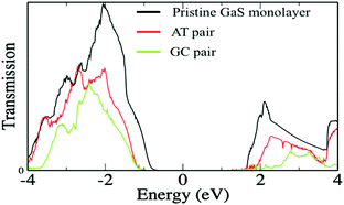 |
| | Fig. 10 Zero-bias transmission spectra of the pristine GaS monolayer (black line), DNA nucleobase pair molecules AT (red line), and GC (green line) adsorbed on the GaS monolayer. | |
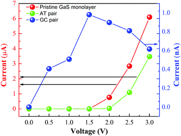 |
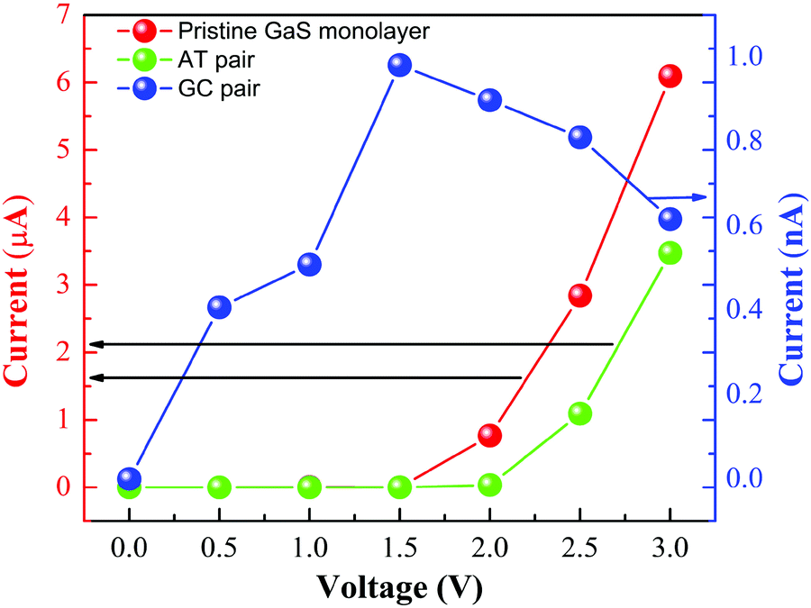
| | Fig. 11 Current–voltage characteristics of (a) pristine GaS monolayer (Redline), AT pair molecules of DNA nucleobase adsorbed on the GaS monolayer (green line) presented on the y-axis with red color (left-side) and GC pair molecules of the DNA nucleobase absorb on the GaS monolayer (blue line) presented on the y-axis with blue color (right-side). | |
Now, we have systematically designed the GaS system with DNA nucleobase sensing characteristics, where DNA nucleobase pairs AT and GC detections can be achieved by the corresponding current–voltage (I–V) relations, which is beneficial to simulate the I–V curves. In Fig. 11, I–V qualities for both the AT and GC pairs with the GaS sheet have been summarized. As a result, the pristine GaS system shows almost no Ohmic behaviors through the current characteristics26 in which there is current passing through the center scattering region that showed increasing behaviour when the bias voltage was applied with the interval of 0.5 V due to the presence of semiconducting behavior. Fig. 11 shows the I–V curves for pristine as well as AT and GC pairs varying up to 3.0 V. When the DNA nucleobase pairs AT and GC molecules interact with the GaS surface, then the current suppressed as compared to the pristine GaS monolayer. Because with the interaction of DNA nucleobase pairs, AT and GC molecules will increase the resistance of the GaS monolayer. This is why the current is suddenly suppressed in DNA nucleobase pairs AT and GC that interact with the GaS sheet. In case of the AT pair, the current increases linearly above 2.0 V because it has less binding energy and charge transfer between the GaS sheet and the AT pair. On the other hand, in case of a GC pair, it has strong binding energy and more charge-transfer, which is why it produces more resistance in the GaS sheet, which decreases the current as compared to pristine GaS and shows non-linear behavior in the I–V characteristics. Remarkably, the current is found to decrease at specific values of the bias voltage, which represents the negative differential resistance (NDR). NDR is an essential property for fast switching of the nanodevices. For the detection of DNA nucleobase pairs AT and GC, a clear distinction can be made. In the case of DNA nucleobases, pairs AT and GC appear to have different resistance and can be easily distinguishable. With and without DNA nucleobases pairs AT and GC molecules, are clearly expressed in terms of distinct current signals that can be observed as ON and OFF states for this device. The sizable distinction in the current signals by properties of DNA nucleobase pairs AT and GC adsorption can be the premise of a predominant GaS based detecting device with better sensitivity. In this association, it is essential to take note of the performance of some other 2D materials such as graphene in which beyond 0.4 V, there is a rapid decrement in the current with the increase in bias voltage reported earlier for DNA nucleobase detection.27,28 According to this, a 2D GaS monolayer has superior features for detecting and modelling sensing nanodevices.
Conclusion
We have systematically inspected the adsorption and transport characteristics of nucleobases on a monolayer GaS surface by employing the vdW-DFT. These studied single nucleobases and pairs have peculiar interaction with the GaS surface with specific electron transfer in the range of 0.02 e to 1.10 e from the adsorbed molecules to the GaS surface. The absorption strength for these nucleobase molecules is in the order G > T > A > C. The individual work function shift signatures for nucleobases were in the range of 0.20 eV to 0.97 eV, which may have promising implications for nucleobase identifications. Further, we have confirmed that the bandgap of the GaS monolayer can be significantly reduced with the adsorption of nucleobase molecules. Also, substantial distinction in the current signals by transport properties of DNA nucleobases pairs AT and GC molecules adsorption can be the premise of a predominant GaS based detecting device with better sensitivity. From these theoretical investigations, it can be depicted that the monolayer GaS surface can be an imminent fortuity for DNA sequencing nanodevice. Furthermore, in the future, the monolayer GaS surface can be attributed to a solid-state nanopore sequencing device where possibilities to detect dsDNA with sugar and phosphate groups attached under different electric fields can be explored.
Conflicts of interest
There are no conflicts to declare.
Acknowledgements
We acknowledge the Carl Tryggers Stiftelse for Vetenskaplig Forskning (CTS), Olle Engkvists stiftelse and Swedish Research Council (VR) for financial support. SNIC and HPC2N are acknowledged for providing the computing facilities.
References
- P. H. Chang, H. Liu and B. K. Nikolić, First-principles versus semi-empirical modeling of global and local electronic transport properties of graphene nanopore-based sensors for DNA sequencing, J. Comput. Electron., 2014, 13, 847–856 CrossRef CAS.
- Y. Ma, Y. Dai, M. Guo, L. Yu and B. Huang, Tunable electronic and dielectric behavior of GaS and GaSe monolayers, Phys. Chem. Chem. Phys., 2013, 15, 7098 RSC.
- P. Hu, L. Wang, M. Yoon, J. Zhang, W. Feng, X. Wang, Z. Wen, J. C. Idrobo, Y. Miyamoto, D. B. Geohegan and K. Xiao, Highly Responsive Ultrathin GaS Nanosheet Photodetectors on Rigid and Flexible Substrates, Nano Lett., 2013, 13, 1649–1654 CrossRef CAS PubMed.
- D. J. Late, B. Liu, J. Luo, A. Yan, H. S. S. R. Matte, M. Grayson, C. N. R. Rao and V. P. Dravid, GaS and GaSe Ultrathin Layer Transistors, Adv. Mater., 2012, 24, 3549–3554 CrossRef CAS PubMed.
- L. Huang, Z. Chen and J. Li, Effects of strain on the band gap and effective mass in two-dimensional monolayer GaX (X = S, Se, Te), RSC Adv., 2015, 5, 5788–5794 RSC.
- H. R. Jappor and M. A. Habeeb, Optical properties of two-dimensional GaS and GaSe monolayers, Phys. E, 2018, 101, 251–255 CrossRef CAS.
- S. Kouser, A. Thannikoth, U. Gupta, U. V. Waghmare and C. N. R. Rao, 2D-GaS as a Photocatalyst for Water Splitting to Produce H 2, Small, 2015, 11, 4723–4730 CrossRef CAS PubMed.
- D. J. Late, B. Liu, H. S. S. R. Matte, C. N. R. Rao and V. P. Dravid, Rapid Characterization of Ultrathin Layers of Chalcogenides on SiO2/Si Substrates, Adv. Funct. Mater., 2012, 22, 1894–1905 CrossRef CAS.
- S. Yang, Y. Li, X. Wang, N. Huo, J.-B. Xia, S.-S. Li and J. Li, High performance few-layer GaS photodetector and its unique photo-response in different gas environments, Nanoscale, 2014, 6, 2582–2587 RSC.
- J. P. Perdew, K. Burke and M. Ernzerhof, Generalized Gradient Approximation Made Simple, Phys. Rev. Lett., 1996, 77, 3865–3868 CrossRef CAS PubMed.
-
F. Han, Problems in Solid State Physics with Solutions, World Scientific, 2011, vol. 50, pp. 391–396 Search PubMed.
-
K. Mathew and R. G. Hennig, Implicit self-consistent description of electrolyte in plane-wave density-functional theory, 2016, 1–6.
- G. Kresse and J. Furthmüller, Efficiency of ab-initio total energy calculations for metals and semiconductors using a plane-wave basis set, Comput. Mater. Sci., 1996, 6, 15–50 CrossRef CAS.
- S. Grimme, J. Antony, S. Ehrlich and H. Krieg, A consistent and accurate ab initio parametrization of density functional dispersion correction (DFT-D) for the 94 elements H-Pu, J. Chem. Phys., 2010, 132, 154104 CrossRef PubMed.
- G. Román-Pérez and J. M. Soler, Efficient Implementation of a van der Waals Density Functional: Application to Double-Wall Carbon Nanotubes, Phys. Rev. Lett., 2009, 103, 096102 CrossRef PubMed.
- H. J. Monkhorst and J. D. Pack, Special points for Brillouin-zone integrations, Phys. Rev. B: Condens. Matter Mater. Phys., 1976, 13, 5188–5192 CrossRef.
- G. Henkelman, A. Arnaldsson and H. Jónsson, A fast and robust algorithm for Bader decomposition of charge density, Comput. Mater. Sci., 2006, 36, 354–360 CrossRef.
- X. Shen, L. Sun, E. Benassi, Z. Shen, X. Zhao, S. Sanvito and S. Hou, Spin filter effect of manganese phthalocyanine contacted with single-walled carbon nanotube electrodes, J. Chem. Phys., 2010, 132, 054703 CrossRef PubMed.
- A. R. Rocha, V. M. García-Suárez, S. Bailey, C. Lambert, J. Ferrer and S. Sanvito, Spin and molecular electronics in atomically generated orbital landscapes, Phys. Rev. B: Condens. Matter Mater. Phys., 2006, 73, 085414 CrossRef.
- T. Xue, W. Liang, Y. Li, Y. Sun, Y. Xiang, Y. Zhang, Z. Dai, Y. Duo, L. Wu, K. Qi, B. N. Shivananju, L. Zhang, X. Cui, H. Zhang and Q. Bao, Ultrasensitive detection of miRNA with an antimonene-based surface plasmon resonance sensor, Nat. Commun., 2019, 10, 28 CrossRef CAS PubMed.
- H. Vovusha and B. Sanyal, Adsorption of nucleobases on 2D transition-metal dichalcogenides and graphene sheet: a first principles density functional theory study, RSC Adv., 2015, 5, 67427–67434 RSC.
- T. Hussain, H. Vovusha, T. Kaewmaraya, V. Amornkitbamrung and R. Ahuja, Adsorption characteristics of DNA nucleobases, aromatic amino acids and heterocyclic molecules on silicene and germanene monolayers, Sens. Actuators, B, 2018, 255, 2713–2720 CrossRef CAS.
- S.-M. Tabatabaei, M. Pourfath and M. Fathipour, Adsorption characteristics of epigenetically modified DNA nucleobases on single-layer MoS2: A first-principles study, J. Appl. Phys., 2018, 124, 134501 CrossRef.
- J.-H. Lee, Y.-K. Choi, H.-J. Kim, R. H. Scheicher and J.-H. Cho, Physisorption of DNA Nucleobases on h -BN and Graphene: vdW-Corrected DFT Calculations, J. Phys. Chem. C, 2013, 117, 13435–13441 CrossRef CAS.
- L. Kou, T. Frauenheim and C. Chen, Phosphorene as a Superior Gas Sensor: Selective Adsorption and Distinct I–V Response, J. Phys. Chem. Lett., 2014, 5, 2675–2681 CrossRef CAS PubMed.
- J. E. Padilha, R. H. Miwa and A. Fazzio, Directional dependence of the electronic and transport properties of 2D borophene and borophane, Phys. Chem. Chem. Phys., 2016, 18, 25491–25496 RSC.
- J. Li, T. Li, Y. Zhou, W. Wu, L. Zhang and H. Li, Distinctive electron transport on pyridine-linked molecular junctions with narrow monolayer graphene nanoribbon electrodes compared with metal electrodes and graphene electrodes, Phys. Chem. Chem. Phys., 2016, 18(40), 28217–28226 RSC.
- J. Prasongkit, A. Grigoriev, B. Pathak, R. Ahuja and R. H. Scheicher, Theoretical study of electronic transport through DNA nucleotides in a double-functionalized graphene nanogap, J. Phys. Chem. C, 2013, 117(29), 15421–15428 CrossRef CAS.
|
| This journal is © the Owner Societies 2020 |
Click here to see how this site uses Cookies. View our privacy policy here. 
 Open Access Article
 This Open Access Article is licensed under a Creative Commons Attribution-Non Commercial 3.0 Unported Licence
 *a,
Pritam Kumar
Panda
a,
Yogendra Kumar
Mishra
*a,
Pritam Kumar
Panda
a,
Yogendra Kumar
Mishra
 , is the dispersion coefficient,
  is the vdW radius, and f(rij)is the damping function.