
Formation of the Cd2Te2O7 phase induced by chemical etching and its influence on the electrical properties of Au/CdTe contacts†
 *a
and
*a
and
Abstract
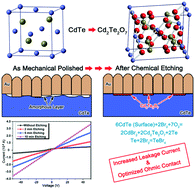
CdTe and related II–VI compound semiconductors have been widely utilized in the field of optoelectronic devices, detectors, solar cells and so on. As the surface treatment on the wafer involved in the device fabrication process has an important impact on its subsequent photoelectric performance, the investigations on the change in structures and properties of the wafer after different surface treatments, especially the formation of new phases at the surface, have important theoretical significance and practical application value. In this work, the surface morphology and microstructure of CdTe single crystal wafers after different chemical etching processes were investigated by atomic force microscopy (AFM), Raman spectroscopy and transmission electron microscopy (TEM). With the increase of etching time to 10 min, the surface gradually became smoother with a significantly reduced surface roughness from 61.4 nm to 30.5 nm. In addition, the I–V curves of Au/CdTe contact structure illustrate the optimized ohmic contact characteristics after chemical etching with the surface leakage current increasing from 4.723 × 10⁻¹⁰ A to 3.640 × 10⁻⁹ A when the etching time extends up to 10 min. TEM analysis on the chemical etched surface of CdTe confirms the formation of Cd2Te2O7 phase with two variants. The d-spacing of (100)CTO and twice that of {111}CdTe being similar is the main reason for the existence of low lattice mismatch and formation of coherent interface between Cd2Te2O7 and CdTe. Furthermore, the chemical etching process is also confirmed to remove the surface damage caused by mechanical polishing effectively by comparing the interface microstructures of Au/CdTe contacts without and after 10 min of chemical etching. The formation mechanism of Cd2Te2O7 and the structure model of Au/CdTe interface are also proposed based on the TEM results.
 Please wait while we load your content...

