
 Open Access Article
 This Open Access Article is licensed under a
 Creative Commons Attribution 3.0 Unported Licence
Impact of various dopant elements on the electronic structure of Cu2ZnSnS4 (CZTS) thin films: a DFT study
Andrey A.
Kistanov
 *a,
Wei
Cao
a,
Marko
Huttula
a,
Salavat Kh.
Khadiullin
b,
Elena A.
Korznikova
c,
Aliaksandr
Smirnov
d,
Xinghui
Wang
e and
Siarhei
Zhuk
d
*a,
Wei
Cao
a,
Marko
Huttula
a,
Salavat Kh.
Khadiullin
b,
Elena A.
Korznikova
c,
Aliaksandr
Smirnov
d,
Xinghui
Wang
e and
Siarhei
Zhuk
d
aNano and Molecular Systems Research Unit, University of Oulu, 90014 Oulu, Finland. E-mail: andrey.kistanov@oulu.fi
bUfa State Aviation Technical University, 450000 Ufa, Russia
cInstitute for Metals Superplasticity Problems, Russian Academy of Sciences, 450001 Ufa, Russia
dBelarusian State University of Informatics and Radioelectronics, 220013 Minsk, Belarus
eCollege of Physics and Information Engineering, Institute of Micro-Nano Devices and Solar Cells, Fuzhou University, Fuzhou 350108, China
First published on 4th August 2020
Abstract
New structures made based on Cu2ZnSnS4 (CZTS) by substitutions with Cr, Ti, V, and Mo species were investigated via density functional theory. The total substitution of Zn by Cr and V leads to the vanishing of the bandgap, while n-type conductivity with a low bandgap of 0.19 eV was predicted in the case Ti. In addition, the conduction band minimum and valence band maximum overlapping were observed for the Mo/Sn ratio of 1/3. Therefore, our study suggests that even the low content of alternative cations in CZTS allows to control its band alignment. The obtained results can be helpful for designing CZTS-based intermediate layers to improve the quality of the back interface of the CZTS thin-film solar cells.
Introduction
Cu2ZnSnS4 (CZTS) thin films have attracted considerable interest in the last decade due to their high potential for the application in photovoltaics.1,2 Suitable optical and electronic properties make CZTS a promising photovoltaic material for the thin-film solar cells.3 The CZTS thin films are characterized by a moderate direct bandgap of 1.5 eV and high absorption coefficient (>104 cm−1) making them interesting candidates for single-junction solar cells.4 Moreover, CZTS possesses intrinsic p-type conductivity due to the presence of Cu vacancies that form shallow acceptor levels.5 In addition, the bandgap of CZTS can be modulated in the range from 1 to 1.5 eV by tuning S/(Se + S) ratio from 0 to 1.6 Furthermore, CZTS thin films demonstrate electronic properties comparable to those of Cu(In,Ga)Se2 (CIGS) films.1 The latter are widely used in the commercial fabrication of highly efficient thin-film solar cells. In contrast to CIGS, rare-earth elements, In and Ga, are replaced with abundant Zn and Sn in CZTS. The highest reported power conversion efficiency (PCE) for CZTSSe solar cells is 12.6%.7On the other hand, champion CIGS and CdTe thin-film solar cells demonstrate PCE of 23.35% and 22.2%, respectively.8 The lack of improvement in the performance of kesterite solar cells is attributed to the defect intolerant nature of the photovoltaic (PV) material.9 The formation of various anti-site defects and clusters of defects is reported for the complex quaternary compound system.10 These defect centers contribute to the recombination and result in low open-circuit voltage (Voc) of kesterite solar cells, which is known to be a major bottleneck limiting the device performance. Moreover, cation-disordering causing the recombination is associated with similar size of cations constituting CZTS.11 Replacing a cation with an isovalent cation of different size is an effective way to suppress the defect formation and reduce the Voc deficit of kesterite solar cells.12 Recent progress in the cation substitution is systematically reviewed in the work of Li et al.13 The incorporation of Ag caused an increase in the bandgap and decrease of carrier concentration.14 The reduced concentration of Ag, in turn, led to an increase in the width of the depletion region.
For CZTS, it has been found that the partial substitution of Zn by Cd causes a decrease in its bandgap and enhancement of the minority carrier lifetime.15,16 Moreover, the Cd substitution allows the fabrication of highly efficient pure sulfide kesterite solar cells prepared using the sputtering and solution-based approach.17 However, the addition of toxic Cd into non-toxic CZTS may limit its application perspectives because of the environmental concern. Another study by Kumar et al. focused on the review of Zn substitution in CZTS.18 Alternatives to Cd such as Mn, Fe, Co, Ni and Ba are examined in the study in detail.
Obviously, experimental brute force methods of searching for the best substituents are expensive, requiring significant labor inputs, and are time-consuming. To suggest the optimal substituents and speed up the progress in the synthesis of high-quality kesterite thin films, atomic simulations are required. The density functional theory (DFT) is the most popular approach in solid-state physics as this method is able to predict the electronic properties of a solid with an excellent ratio of accuracy and computational demand.19–21
In contrast to the above-mentioned studies, which aims to find suitable cation substitution approaches to fabricate CZTS absorber layers of higher quality, the present study demonstrates a way to develop the CZTS-based intermediate layer. CZTS is known for its instability when in contact with Mo at high processing temperatures.22 Detrimental solid-state reactions at the rear contact lead to the void formation due to the evaporation of volatile secondary phases.5,22 Furthermore, the loss of Zn and Sn occurs during sulfurization.5 In addition, voids are reported to increase the series resistance of CZTS solar cells.23 Therefore, ILs are deposited to suppress the reaction at the interface between Mo and CZTS.24 However, the insertion of an IL may lead to the degradation of CZTS crystallinity as the crystal structures of the materials are different.25
In this work, we use first-principles DFT simulations to study the effect of Zn substitution by Cr, Ti, and V. These elements were chosen for the substitution as they are characterized by a significantly higher melting temperature relative to that of Zn with the oxidation state of +2. To the best of our knowledge, no studies on simulation of Cu2CrSnS4, Cu2TiSnS4 and Cu2VSnS4 are reported to date. In addition, in a recent report, we demonstrated a remarkable improvement in the PCE of sputtered CZTS solar cells from 1.6% to 5.5% owing to the Mo incorporation.26 Since evidence of Sn substitution by Mo were observed, in this study, we also investigate the effect of the partial substitution of Sn by Mo on the energy bands distribution using DFT simulations to provide insights enabling more efficient designing of CZTS based absorbers.
Methods
The DFT based first-principles calculations were performed using the plane-wave Vienna ab initio simulation package (VASP).27 The Perdew–Burke–Ernzerhof (PBE) exchange–correlation functional under the generalized gradient approximation28 (GGA) together with the van der Waals corrected functional with Becke88 optimization29 were used for geometry optimization of all structures and band structure calculations of strained Cu2TiSnS4. The electronic structure of the structures with the full substitution of Zn/Sn was considered using the accurate hybrid functional (HSE06). Due to the high computational cost of hybrid functionals, the electronic structure of all the remaining structures (with the partial substitution) was considered using PBE GGA. All the structures are fully relaxed until the atomic forces and total energy values were smaller than 0.01 eV Å−1 and 10−6 eV, respectively. The kinetic energy cutoff of 400 eV was adopted. Periodic boundary conditions were applied in all three directions. The first Brillouin zone was sampled with a 15 × 15 × 8 k-mesh grid. The Mo/Sn ratio was controlled by the substitution of the Sn by Mo atoms.The calculated lattice constants a (b) and c of the considered pure CZTS unit cell (see Fig. 1a) were found to be 5.435 Å and 10.843 Å, respectively. Our results are well compared with experimental30 and theoretical data.31–33 The bandgap size (1.38 eV) calculations for pure CZTS (see Fig. 1b) show high accuracy and are comparable with the theoretical and experimental data (1.4–1.5 eV) reported in a number of works.34–36
 | ||
| Fig. 1 Atomic configuration (a) and band structure (HSE06) (b) of CZTS. The red dashed line represents the Fermi level. | ||
Results and discussion
Firstly, the effect of the partial substitution of Zn by Cr, Ti, and V is considered. Fig. 2a–c show the band (bottom panel) and the atomic (top panel) structures of CZTS with Zn atoms substituted by Cr, Ti, and V atoms, respectively. The study shows the presence of Cr (see Fig. 2a) that leads to the downward shift of the conduction band minimum (CBM) and the upward shift of valance band maximum (VBM). The CBM crosses the Fermi level at the point between Γ and X points, and VBM crosses the Fermi level at the point between nearby the N point, which evidences the closing of the Cu2CrSnS4 bandgap. It should be noted that the partial substitution of Zn by Cr (at the Cr/Zn ratio of 1/1) also leads to the closing of the bandgap (see Fig. 3a). The modification of the CZTS bandgap with the incorporation of Cr was also observed in the experimental study.37 The addition of Cr in CZTS was carried out by the co-sputtering of CZTS and Cr targets. It has been reported that the incorporation of Cr into CZTS performed by the co-sputtering of CZTS and Cr targets modified the bandgap and structural properties of CZTS thin films. With the increase of Cr content from 0 to ∼9%, the bandgap increased from 1.51 eV to 1.7 eV. On the other hand, the bandgap decreased to 1.54 eV when measured Cr was ∼15.8%. Note, that in contrast to the study of Sapeli et al., the case of the full substitution of Zn by Cr is simulated in this report.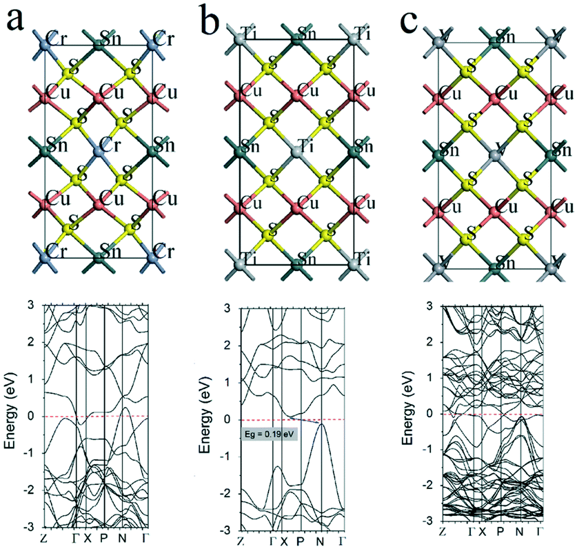 | ||
| Fig. 2 Atomic configuration and band structure (HSE06) of (a) Cr-, (b) Ti-, and (c) V-doped CZTS. The red dashed lines represent the Fermi level. | ||
 | ||
| Fig. 3 Band structure (GGA PBE) of (a) Cr-, (b) Ti-, and (c) V-doped CZTS. From the left to the right the concentration of dopants is 0%, 50%, and 100%. The black dashed lines represent the Fermi level. | ||
The substitution of Zn by Ti also induces the shift of CBM towards VBM and a shift of CBM from the Γ point to the point between the X and P points and VBM shifts from the Γ point to the N point. As a result, the indirect bandgap of 0.19 eV was observed for Cu2TiSnS4 (see Fig. 2b). It can also be seen that the compound demonstrates n-type conductivity, unlike CZTS. It may be expected that by controlling the Zn/Ti ratio, it is possible to tune not only the bandgap of Cu2TiSnS4 but also band alignment by manipulating CBM and VBM bands. Indeed, Fig. 3b shows that with an increase in the concentration of Ti from 0% to 50%, the band alignment significantly changes, which leads to the shift of CBM and VBM and the closure of the bandgap. Furthermore, the use of ultrathin Cu2TiSnS4 instead of the CdS buffer layer may be useful to passivate the hetero-interface and reduce the density of defects, and thus, improve the open-circuit voltage deficit.
The simulation study reveals that the substitution of Zn by V causes strong band mixing, which leads to the vanishing of the bandgap (see Fig. 2c). This suggests a metallic-like behavior of Cu2VSnS4. As shown in Fig. 3c, even the partial substitution of Zn by V leads to the formation of a metallic-like Cu2VSnS4 structure. Thus, it can be concluded that the full substitution of Zn by alternative cations (Cr, Ti, and V) is not suitable for the fabrication of thin-film absorbers due to the low bandgap or its absence. By the interpolation of the obtained results, the existence of bandgap for a low ratio of the substituted cations can be expected. Moreover, the cation substitution with Cr, Ti, and V was found to be effective in tuning CBM and VBM. Hence, these alternative cations may be used to provide tools for adjusting band alignment at the back and front interfaces of the CZTS absorber layer if used in a relatively small amount.
Owing to the observed metallic-like properties of Cu2CrSnS4 and Cu2VSnS4, these materials can be used as IL to improve the ohmic contact between the CZTS absorber layer and Mo back contact. Furthermore, as Cu2CrSnS4 and Cu2VSnS4 possess the same crystal structure as CZTS, they can serve as a seed layer to enhance CZTS crystal growth and reduce the density of defects. Moreover, the deposition of Cu2CrSnS4 and Cu2VSnS4 IL at the back interface may reduce the void formation as the loss of volatile elements during sulfurization is suppressed. Therefore, the series resistance of the solar cells can be reduced with the reduced voids at the back interface.
Next, the effect of the partial substitution of Sn by Mo is investigated. More detailed consideration is addressed to the substitution of Sn by Mo as in our recent study the positive effect of Mo incorporation into sputtered CZTS has been shown.26 To investigate the impact of the Mo content on the band structure of CZTS some of the Sn atoms are replaced with Mo atoms. Fig. 4 and 5 show the atomic configurations and band structures, respectively, of pristine and Mo-doped CZTS.
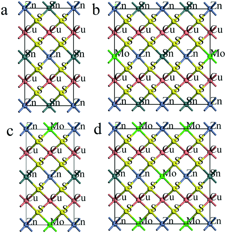 | ||
| Fig. 4 Atomic configuration of Mo-doped CZTS for the Mo/Sn ratio of (a) 0, (b) 1/3, (c) 1/1 and (d) 3/1. The Cu, Zn, Sn, S, and Mo atoms are colored in red, violet, gray, yellow and green, respectively. | ||
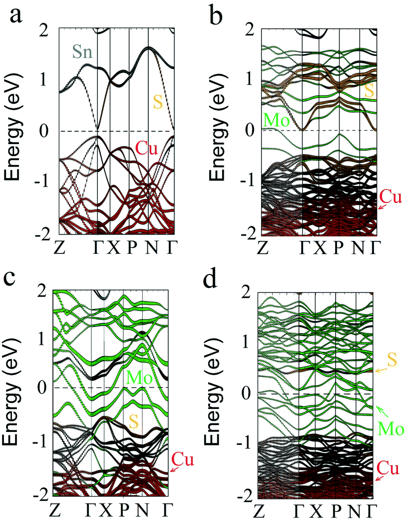 | ||
| Fig. 5 Band structure (GGA PBE) of Mo-doped CZTS for the Mo/Sn ratio of (a) 0, (b) 1/3, (c) 1/1 and (d) 3/1. The bands corresponding to Cu, Zn, Sn, S, and Mo atoms are colored in red, violet, gray, yellow and green, respectively. The horizontal black line represents the Fermi level. | ||
Surprisingly, at the Mo/Sn ratio of 1/3, the bandgap shrinks to zero (see Fig. 5b) because the valence and conduction bands are crossing the Fermi level between the Γ and Z points, which supposes the formation of metal-like CZ(Sn0.75Mo0.25)S. Importantly, there is still an energy gap between the X and N points. Further, with an increase in the Mo content (up to the full substitution of Sn by Mo) in CZTS its bandgap vanishes due to the overlapping of valence and conduction bands, as shown in Fig. 5c and d.
To deeply understand changes taking place within the energy gap of CZTS upon Mo doping, the local density of states (LDOS) analysis of pristine and Mo-doped CZTS was also conducted (see Fig. 6). As shown in Fig. 6b, at the Mo/Sn ratio of 1/3, Mo states are significantly broadened and strongly mixed with the states of the host material. In addition, the upward shift of Sn states is observed. An increase of Mo concentration leads to the further shift of Sn states and the appearance of Mo states within the energy gap. Importantly, the spin splitting and broadening of Mo states increase with the increasing concentration (see Fig. 6c and d). An interesting feature of Mo-doped CZTS is that only spin up states (all are Mo states) are occupied below the Fermi level, which may be responsible for its enhanced light-harvesting ability.
 | ||
| Fig. 6 LDOS of Mo-doped CZTS for the Mo/Sn ratio of (a) 0, (b) 1/3, (c) 1/1 and (d) 3/1. The bands corresponding to Cu, Zn, Sn, S, and Mo atoms are colored in red, violet, gray, yellow and green, respectively. The vertical black lines represent the Fermi level. | ||
Using interpolation of the results we may expect the existence of the bandgap for CZTS with the Mo/Sn ratio in the range from 0 to 1/3. Formation of metallic-like CZTS supports observed reduction in resistivity of the CZTS thin films as a result of Mo incorporation in our recent experimental work.26 In addition, this may also explain the enhanced fill factor of Mo-incorporated CZTS solar cells by the formation of better ohmic contact at the CZTS/Mo interface.
The simulation data presented in Fig. 6 provides an additional explanation of the phenomena of the increased light absorbance for Mo-incorporated CZTS thin films reported in our experimental study.26 Given the short minority charge carrier diffusion length in CZTS,38 the fabrication of the solar cells with an ultrathin absorber layer is useful to enhance charge collection efficiency. Therefore, the improvement of light absorption in CZTS thin films via the alternative cation incorporation is critical for the ultrathin absorber layer to maintain the harvesting of a reasonable portion of incident photons. For this reason, it may contribute to the overall improvement of CZTS solar cell performance. In addition, improved understanding of the nature of the increase in the conductivity of Mo-substituted CZTS thin films, allows the designing of CZTS solar cells with a back surface field where Mo-substituted CZTS is used as IL to reduce recombination at the back interface and improve charge transport.39
Conclusions
The study demonstrated that new compounds such as Cu2CrSnS4, Cu2TiSnS4, Cu2VSnS4 and Cu2Zn(Snx,Mo1−x)S4 can be formed. It has been revealed that the full substitution of Zn in CZTS results in the closing of the bandgap for the case of Cu2CrSnS4 and Cu2VSnS4, while the overlapping of CBM and VBM was observed at the Mo/Sn ratio of 1/3. In addition, n-type Cu2CrSnS4 with a low bandgap of 0.19 eV was simulated. This study shows that the relatively low content of alternative cations in the CZTS absorber layer significantly affects the distribution of energy levels in conduction and valence bands, thus providing additional ways to control band alignment.The obtained results can be useful for designing CZTS solar cells with IL based on the same crystal structure. First, highly conductive Cu2CrSnS4, Cu2VSnS4 and Cu2Zn(Snx,Mo1−x)S4 ILs can be used to improve the ohmic properties of the back contact. In addition, these IL may address the problem of the increased series resistance of the solar cells due to the presence of voids at the back interface. Second, since these new compounds exhibit the same crystal structure as CZTS, they can be used as a seed layer to facilitate the growth of high-quality CZTS absorber layer. Third, the substitution of Zn and Sn by elements with much higher melting temperatures may suppress its loss from the CZTS absorber layer during high-temperature sulfurization as the elemental loss causes the formation of anti-site defects and vacancies.
Conflicts of interest
There are no conflicts to declare.Acknowledgements
The authors acknowledge CSC–IT Center for Science, Finland, for computational resources. A. A. Kistanov, W. Cao, and M. Huttula acknowledge the financial support provided by the Academy of Finland (grant No. 311934).References
- X. Liu, Y. Feng, H. Cui, F. Liu, X. Hao, G. Conibeer, D. B. Mitzi and M. Green, Prog. Photovolt: Res. Appl., 2016, 24, 879–898 CrossRef
.
- S. A. Khalate, R. S. Kate and R. J. Deokate, Sol. Energy, 2018, 169, 616–633 CrossRef CAS
-
K. Ito, Copper zinc tin sulfide-based thin-film solar cells, Wiley, Chichester, 2015 Search PubMed
- D. B. Mitzi, O. Gunawan, T. K. Todorov, K. Wang and S. Guha, Sol. Energy Mater. Sol. Cells, 2011, 95, 1421–1436 CrossRef CAS
- M. Kumar, A. Dubey, N. Adhikari, S. Venkatesan and Q. Qiao, Energy Environ. Sci., 2015, 8, 3134–3159 RSC
- J. He, L. Sun, S. Chen, Y. Chen, P. Yang and J. Chu, J. Alloys Compd., 2012, 511, 129–132 CrossRef CAS
- W. Wang, M. T. Winkler, O. Gunawan, T. Gokmen, T. K. Todorov, Y. Zhu and D. B. Mitzi, Adv. Energy Mater., 2014, 4, 1–5 Search PubMed
- M. A. Green, E. D. Dunlop, D. H. Levi, J. Hohl-Ebinger, M. Yoshita and A. W. Y. Ho-Baillie, Prog. Photovoltaics, 2019, 27, 565–575 Search PubMed
- S. Siebentritt, Thin Solid Films, 2013, 535, 1–4 CrossRef CAS
- S. Chen, A. Walsh, X. G. Gong and S. H. Wei, Adv. Mater., 2013, 25, 1522–1539 CrossRef CAS PubMed
- S. Bourdais, C. Choné, B. Delatouche, A. Jacob, G. Larramona, C. Moisan, A. Lafond, F. Donatini, G. Rey, S. Siebentritt, A. Walsh and G. Dennler, Adv. Energy Mater., 2016, 6, 1502276 CrossRef
- C. Yan, K. Sun, J. Huang, S. Johnston, F. Liu, B. P. Veettil, K. Sun, A. Pu, F. Zhou, J. A. Stride, M. A. Green and X. Hao, ACS Energy Lett., 2017, 2, 930–936 CrossRef CAS
- J. Li, D. Wang, X. Li, Y. Zeng and Y. Zhang, Adv. Sci., 2018, 5, 1700744 CrossRef PubMed
- A. Guchhait, Z. Su, Y. F. Tay, S. Shukla, W. Li, S. W. Leow, J. M. R. Tan, S. Lie, O. Gunawan and L. H. Wong, ACS Energy Lett., 2016, 1, 1256–1261 CrossRef CAS
- Z. Su, J. Ming, R. Tan, X. Li, X. Zeng, S. K. Batabyal and L. H. Wong, Adv. Energy Mater., 2015, 5, 1500682 CrossRef
- S. H. Hadke, S. Levcenko, S. Lie, C. J. Hages, J. A. Márquez, T. Unold and L. H. Wong, Adv. Energy Mater., 2018, 8, 1802540 CrossRef
- J. Fu, Q. Tian, Z. Zhou, D. Kou, Y. Meng, W. Zhou and S. Wu, Chem. Mater., 2016, 28, 5821–5828 CrossRef CAS
- M. S. Kumar, S. P. Madhusudanan and S. K. Batabyal, Sol. Energy Mater. Sol. Cells, 2018, 185, 287–299 CrossRef CAS
-
W. Koch and M. C. Holthausen, A chemist's guide to density functional theory, Wiley-VCH, 2001 Search PubMed
- P. P. Sun, D. R. Kripalani, L. C. Bai and K. Zhou, J. Phys. Chem. C, 2019, 123, 12684–12693 CAS
- P. P. Sun, D. R. Kripalani, M. Hao, W. Chi, W. Li and K. Zhou, J. Phys. Chem. Lett., 2020, 11, 5234–5240 CrossRef CAS PubMed
- J. J. Scragg, T. Ericson, T. Kubart, M. Edoff and C. Platzer-Björkman, Chem. Mater., 2011, 23, 4625–4633 CrossRef CAS
- W. Li, J. Chen, H. Cui, F. Liu and X. Hao, Mater. Lett., 2014, 130, 87–90 CrossRef CAS
- S. Zhuk, T. K. S. Wong, M. Petrovic, E. Kymakis, S. S. Hadke, S. Lie, L. H. Wong, P. Sonar, A. Dey, S. Krishnamurthy and G. K. Dalapati, Sol. RRL, 2020, 2000293 CrossRef
- S. Zhuk, T. K. S. Wong, E. Tyukalova, A. Guchhait, D. H. L. Seng, S. Tripathy, T. I. Wong, M. Sharma, H. Medina and G. K. Dalapati, Appl. Surf. Sci., 2019, 471, 277–288 CrossRef CAS
- S. Zhuk, T. K. Sh. Wong, S. Sudhakar, S. Lie, A. Guchhait, Y. Gao, L. Helena, S. Cheng and X. Wang, Sol. Energy, 2019, 194, 777–787 CrossRef CAS
- G. Kresse and J. Furthmüller, Phys. Rev. B: Condens. Matter Mater. Phys., 1996, 54, 11169 CrossRef CAS PubMed
- J. P. Perdew, K. Burke and M. Ernzerhof, Phys. Rev. Lett., 1996, 77, 3865–3868 CrossRef CAS PubMed
- A. D. Becke, Phys. Rev. A: At., Mol., Opt. Phys., 1988, 38, 3098 CrossRef CAS PubMed
- S. R. Hall, J. T. Szymanski and J. M. Stewart, Kesterite, Can. Mineral., 1978, 16, 131 CAS
- J. Paier, R. Asahi, A. Nagoya and G. Kresse, Phys. Rev. B: Condens. Matter Mater. Phys., 2009, 79, 115126 CrossRef
- S. Chen, X. G. Gong, A. Walsh and S. H. Wei, Appl. Phys. Lett., 2010, 96, 021902 CrossRef
- A. J. Jacksona and A. Walsh, J. Mater. Chem. A, 2014, 2, 7829–7836 RSC
- J. Chen, F. Wang, B. Yang, X. Peng, Q. Chen, J. Zou and X. Dou, Coatings, 2019, 9, 130 CrossRef
- H. Katagiri, K. Jimbo, W. S. Maw, K. Oishi, M. Yamazaki, H. Araki and A. Takeuchi, Thin Solid Films, 2009, 517, 2455–2460 CrossRef CAS
- M. Y. Yeh, P. H. Lei, S. H. Lin and C. D. Yang, Materials, 2016, 9, 526 CrossRef PubMed
- M. M. I. Sapeli, M. T. Ferdaous, S. A. Shahahmadi, K. Sopian, P. Chelvanathan and N. Amin, Mater. Lett., 2018, 221, 22–25 CrossRef CAS
- S. Zhuk, A. Kushwaha, T. K. S. Wong, S. Masudy-Panah, A. Smirnov and G. K. Dalapati, Sol. Energy Mater. Sol. Cells, 2017, 171, 239–252 CrossRef CAS
- A. E. H. Benzetta, M. Abderrezek and M. E. Djeghlal, Optik, 2019, 181, 220–230 CrossRef CAS
| This journal is © The Royal Society of Chemistry 2020 |