
Tuning of the morphological and electronic properties of In2S3 nanosheets by cerium ion intercalation for optimizing photocatalytic activity†
Soumya Shankar
Basu
,
Sibsankar
Rahut
 ,
Charishma
Chinthala
and
Jayanta Kumar
Basu
*
,
Charishma
Chinthala
and
Jayanta Kumar
Basu
*
Department of Chemical Engineering, Indian Institute of Technology, Kharagpur, India. E-mail: basuhitk@gmail.com; jkb@che.iitkgp.ernet.in; Tel: +91 3222 283914
First published on 15th June 2020
Abstract
In this work, a facile hydrothermal treatment has been followed to develop In2S3 nanosheets doped with 0–2 mol% cerium. Morphological and structural analyses have revealed the development of highly crystalline smooth In2S3 nanosheets upon 1 mol% cerium doping. The substitutionally doped cerium ions have led to hybridization of the Ce 4f and In 5p orbitals resulting in downshift of the conduction band edge thus aiding in higher photon absorption for enhanced photocatalytic activity. Such characteristics have been deduced from the UV-vis spectra and further theoretically verified by employing first principles density functional theory (DFT) calculations to obtain density of states (DOS) plots of computationally constructed 1 mol% Ce doped In2S3 structures. Transient photocurrent responses have been obtained and photocatalytic degradation of neurotoxic drug ciprofloxacin has been performed to demonstrate the enhanced photocatalytic and photoelectrocatalytic potential of cerium doped samples. The marked improvement showed a rapid decline in the 2 mol% Ce doped samples, due to the limited solubility of cerium ions in the In2S3 lattice leading to structural deformities upon excess cerium doping. Thus, the synergistic influence of indium and cerium atoms in In2S3 nanocompounds for solar energy applications has been established by various experimental analyses complemented with theoretical investigations via DFT calculations.
Introduction
Ever since the photoelectrochemical water splitting experiment demonstrated by Fujishima and Honda in 1972, there has been extensive research across the globe to utilize solar energy for electrochemical/photochemical reactions. The depletion of nonrenewable sources of energy and severe environmental pollution has provided further impetus to the quest for utilizing renewable sources of energy, like solar energy, for energy production and environmental remediation. In this context, photocatalysis is a technique which has garnered tremendous attention due to its vast applications in H2 energy production,1 wastewater treatment,2 gas sensing,3etc. Photocatalysts are materials which can harness solar energy to produce electrons and holes, which drive the photocatalytic reactions towards their desired objectives.In the last decade, scientists and researchers across the world have developed several such photocatalysts, the foremost being TiO2 (ref. 4) and ZnO.5 However these materials have a wide band gap of 3.0–3.4 eV limiting their applicability in the presence of just UV light, in the solar spectrum. Thereafter, there has been immense focus on the development of narrow band gap visible light active photocatalysts, like BiVO4,6 Ag3PO4,7 Bi2WO6,8 Ag3VO4,9etc. In this context, chalcogenides like In2S3,10–12 ZnIn2S4 (ref. 13) and Bi2S3 (ref. 14) have exhibited strong photocatalytic activity due to their unique optoelectronic properties. In particular, indium sulphide (In2S3) has been of much interest to researchers because of its advantageous properties like excellent photostability, visible light activity and low toxicity.12
A group III–VI sulphide, In2S3 exists in 3 polymorphic forms at room temperature, i.e. the defective cubic structure α-In2S3 (stable up to 693 K), a defective spinel structure called β-In2S3 (stable up to 1027 K), and the higher temperature layered structure γ-In2S3 (above 1027 K).15 Among these, spinel structure β-In2S3 has garnered maximum attention due to its visible light active band gap (2–2.3 eV), stability at room temperature and promising results with regard to applications in photovoltaic solar cells16,17 and photocatalytic dye degradation.18,19 Since the morphological characteristics of the photocatalysts determine their electronic configuration and charge carrier generation, researchers have developed In2S3 samples in several architectures like 3D-flower like structures,20 microspheres,19 nanobelts21 and nanosheets,22 in order to further enhance the photocatalytic activity. Doping semiconductor nanocompounds with foreign metal ions is another means of optimizing their electronic properties23 and in this regard, research has been conducted on In2S3 nanocrystals doped with metals like Zr,24 Sn,25 Co,26 V (ref. 27) and Ca.28 In all those reports, the doped In2S3 samples showed enhanced photocatalytic activity, thus proving improved visible light harvesting and charge separation upon the incorporation of foreign metal ions in the In2S3 lattice. However, there are a few other common metal ion dopants whose influence on the photocatalytic activity of In2S3 has not been explored yet. Cerium (Ce) is one such dopant which has significantly improved the photocatalytic activity of conventional metal oxide photocatalysts like TiO2 (ref. 29) and BiVO4.30 Cerium is an inexpensive nontoxic lanthanide element which can exist in the Ce3+ or Ce4+ atomic state, leading to electronic reconfiguration and band gap tuning in the photocatalysts. The partially populated 4f states in the Ce3+ ions have introduced new energy states in the optical band gaps of metal oxides resulting in the capability to harness a greater part of the solar spectrum and achieve enhanced electron–hole separation. The synergistic influence of cerium and indium atoms on sulphides has not been reported yet, and hence, it is desirable to investigate the effect of Ce doping on the structural and electronic properties of In2S3.
Herein, we report the effect of cerium ion doping on the morphological and optoelectronic properties of β-In2S3. Wafer thin 2D In2S3 nanosheets doped with Ce ions have been developed by a facile hydrothermal method. The concentration of Ce ions has been varied to investigate its influence on the In2S3 samples. This has been followed by extensive characterization, in order to study the effects of cerium ion intercalation and determine the most optimum dopant dosage for photocatalytic applications. Our analyses revealed that the substitutionally doped cerium ions enhanced the spectral response leading to maximum photocatalytic activity and photocurrent generation in the 1 mol% doped samples. To complement our experimental findings, first principles DFT calculations have been performed to theoretically generate the electronic and crystal structures of the doped In2S3 samples. The experimental and theoretical results have been analyzed in tandem to gain deeper insights into the effects of cerium ion insertion in the In2S3 lattice.
Results and discussion
The pristine In2S3 sample is labelled InS, and the samples doped with 0.5 mol%, 1 mol% and 2 mol% cerium are labelled 0.5C-InS, 1C-InS and 2C-InS, respectively.Structural characterization
X-Ray diffractograms were recorded to investigate the crystalline frameworks of the developed samples. From the distinct peaks in the X-ray diffractograms presented in Fig. 1a, we can conclude the development of highly crystalline samples. The XRD patterns of pristine In2S3 samples are well in agreement with those of tetragonal In2S3 (PDF# 00-051-1160). We can observe distinct peaks at 2θ values of 14.5°, 27.5°, 33.37°, 43.82°, and 47.8° corresponding to the (103), (213), (220), (309) and (400) facets of tetragonal In2S3, respectively. 0.5C-InS samples showed no conspicuous new peaks indicating that the Ce atoms underwent substitutional doping and did not alter the crystalline framework. However, upon increasing the Ce dopant dosage to 1%, we can observe 2 new peaks at 23.1° and 38.15°. Moreover a weak peak visible at 56.14° in the InS and 0.5C-InS samples has become much more prominent in the 1C-InS sample. These peaks correspond to the (200), (305), and (419) facets, respectively, of tetragonal In2S3, suggesting an improved crystalline structure upon doping with 1% Ce. It can be deduced that these facets which have developed only in the 1C-InS samples have played an important role in the development of the 2D nanosheets as observed in FESEM images. Likewise, a tiny peak observed at 28° in the 0.5C-InS sample has gained more prominence in the 1C-InS sample. This can be indexed to the (031) facet in orthorhombic Ce2S3 (PDF# 430800). The development of this particular facet of Ce2S3 has been observed in HRTEM images of lattice fringes, as discussed later. However, the new peaks developed in the 1C-InS samples lost their prominence upon increasing the Ce dosage to 2%. We can see weak peaks corresponding to the (305) and (419) facets, while the peak corresponding to the (200) facet disappeared. The peak corresponding to the (031) facet of Ce2S3 also became smaller and broader in the 2C-InS samples, indicating weaker crystallinity. It can be deduced that upon increasing the Ce dosage beyond a limit, the intercalating Ce ions impede the development of tetragonal In2S3 and orthorhombic Ce2S3 crystalline networks. Hence, the 2C-InS samples revealed an uneven diffuse morphology in FESEM images.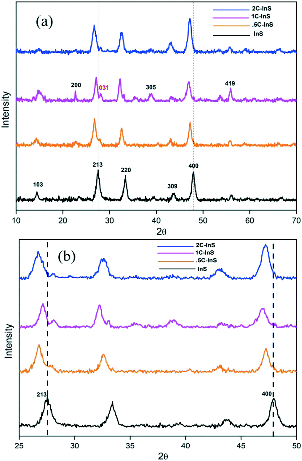 | ||
| Fig. 1 (a) X-Ray diffractograms of the developed samples. (b) Magnified view of peak shifts. | ||
Another important observation is the slight left shift of the peaks corresponding to the (213) and (400) facets (Fig. 1b), suggesting cell volume expansion upon cerium doping. This can be explained by the fact that the ionic radius of Ce3+ atoms (1.03 Å) is higher than that of In3+ (0.9 Å) resulting in higher crystallite sizes in the doped samples. This is further confirmed by calculation of the average crystallite sizes following the modified Debye–Scherrer equation,31 as presented in Table 1. Upon doping, a slight increment in crystallite sizes can be observed. This is well in accordance with the decreasing values of the BET surface area with increasing crystallite sizes. There have been similar reports on doping In2S3 with Ca and Ag atoms.32 Moreover, the crystallite sizes are in good agreement with the thickness of the nanosheets observed in the FESEM images. The lattice parameters a and c of the synthesized samples have been calculated considering the d-spacing values of the distinct (213) and (400) facets using the following established formula for tetragonal systems:
 | (1) |
| Sample | Pore dia. (nm) | Pore vol. (cc g−1) | Crystal size (nm) | BET surface area (m2 g−1) | Lattice parameter a (Å) | Lattice parameter c (Å) | Cell vol. (Å3) |
|---|---|---|---|---|---|---|---|
| InS | 13.31 | 0.25 | 76.73 | 15.62 | 7.600 | 31.961 | 1846.06 |
| 0.5C-InS | 14.26 | 0.24 | 67.48 | 16.92 | 7.661 | 31.982 | 1877.05 |
| 1C-InS | 20.26 | 0.225 | 58.41 | 18.68 | 7.688 | 35.873 | 2120.26 |
| 2C-InS | 28.53 | 0.225 | 41.41 | 19.96 | 7.691 | 37.291 | 2205.82 |
FTIR spectra of the InS and 1C-InS samples were recorded to investigate the nature of chemical bonds present (Fig. S1, ESI†). All samples showed similar trends with the 0.5C-InS, 1C-InS and 2C-InS samples showing a peak at 505 cm−1. This can be attributed to stretching vibration of the Ce–S bond.33 This peak appears to have broadened and lost its sharpness in the 2C-InS samples, probably due to excessive cerium doping. The peak visible at 780 cm−1 in pristine InS can be attributed to In–S bond stretching.34 It can be observed that this peak has undergone a slight left shift to 710 cm−1 in the doped samples. This can be attributed to the effects of intercalating Ce ions within the In–S networks. The peak at 1070 cm−1 can be attributed to stretching vibrations of the C![[double bond, length as m-dash]](https://www.rsc.org/images/entities/char_e001.gif) S bond arising from adsorbed CO2 molecules. The peaks at 1621 cm−1 and 3314 cm−1 have appeared due to bending and stretching vibrations of adsorbed OH groups, respectively.
S bond arising from adsorbed CO2 molecules. The peaks at 1621 cm−1 and 3314 cm−1 have appeared due to bending and stretching vibrations of adsorbed OH groups, respectively.
Morphological characterization
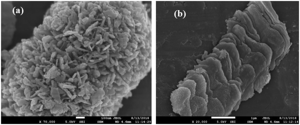
FESEM images have been recorded and analyzed to determine the morphological characteristics of the developed samples. From the images of InS samples presented in Fig. 2a, we can observe flake-like nanoparticles bundled together resembling a flower-like architecture. On closer inspection, we can observe the development of wafer thin nanosheets with a thickness ranging from 13–15 nm (Fig. 2b), which are closely intertwined to form microflowers having a diameter of around 800 nm. The development of flower-like β-In2S3 structures upon surfactant assisted synthesis is in good agreement with previous reports.20 There is no distinct change in morphology upon doping 0.5% Ce (Fig. 2c). The microflowers look more compact, having a diameter of around 450 nm, while the densely clustered nanosheets constituting the microflowers have slightly gained thickness, ranging from 13–17 nm. This can be attributed to unit cell expansion upon cerium doping, which was also established earlier from the XRD analysis. As observed in Fig. 2d, the magnified image reveals flake-like surfaces which might represent the cross sectional facets of nanosheets. The development of 2D nanosheets upon cerium ion intercalation can be further verified by increasing the amount of cerium doping to 1%. In Fig. 2e and f, distinct nanosheets with irregular dimensions ranging from 200–350 nm can be clearly observed in the 1C-InS samples. These ultrathin nanosheets have the potential of functioning as a smooth short pathway for efficient charge carrier separation.35,36 Such morphological characteristics have been further validated by obtaining TEM images for the 1C-InS sample. Distinct sheet-like structures with distinguishable grain boundaries are clearly visible in the images presented in Fig. 3a and b. Each sheet is clearly visible despite some being stacked upon each other, thereby confirming their ultrathin dimensions. The intercalation of Ce3+ ions in between the pristine In2S3 bundles and their strong electrostatic force with the S2− ions have led to the thermodynamic stabilization of the nanosheet surfaces. The interactions between the metal ions and the complex functional groups present along the L-cysteine surfactant chains can also be reasoned to have prevented the formation of flowerlike agglomerates. | ||
| Fig. 2 FESEM images of (a and b) pristine InS and (c) 0.5C-InS. (d) Magnified views of 0.5C-InS and (e and f) 1C-InS. | ||
 | ||
| Fig. 3 (a and b) TEM images, (c) high magnification HRTEM image of the lattice fringes and (d) SAED pattern of 1C-InS. | ||
The rings formed by bright spots in the SAED pattern suggest a highly nanocrystalline sample (Fig. 3d). The rings have been indexed to the (213), (400), and (419) planes of tetragonal In2S3. The development of such facets has been further established upon analyzing the X-ray diffractogram of 1C-InS, as discussed earlier. Lattice fringes corresponding to the (213), (400) and (305) facets are observable in the HR-TEM images (Fig. 3c). It is also observable that the (400) facet is intersected perpendicularly by another lattice fringe. This right angled cross fringe can be ascribed to the (031) facet in orthorhombic Ce2S3, suggesting slight formation of Ce–S bonds due to substitutional doping of Ce atoms in the 1C-InS sample. The lattice fringe corresponding to the (031) facet is again observable, making an angle of 72° with the fringe corresponding to the (305) facet of cubic In2S3. A tiny peak corresponding to the (031) facet of Ce2S3 was noticed in the X-ray diffractogram as well, as discussed earlier. Nanosheet like clusters are also visible in the 2C-InS samples. However, on closer inspection, the 2C-InS samples revealed two distinct types of morphology: 1) nanosheets as observed previously stacked onto one another, without proper distinguishable grain boundaries (Fig. 4a); 2) nanoflakes ranging from 15–35 nm in thickness clustered into flower-like bundles (Fig. 4b). The development of 2 types of nanoparticles may be attributed to phase separation of In2S3 nanoparticles at high Ce concentration during hydrothermal treatment, from which we further deduce that cerium has limited solubility in tetragonal β-In2S3. Thus, it can be concluded that cerium dopant ions play an important role in controlling the growth and morphology of In2S3 nanoparticles.
 | ||
| Fig. 4 (a and b) FESEM images of 2C-InS. | ||
The atomic composition of the developed samples was determined by EDX analysis and is reported in Table S2, ESI.† It can be observed that the atomic percentage of indium undergoes a slight decline with increasing cerium dopant concentration, possibly due to cerium atoms substituting indium atoms in the In2S3 lattice. The molar amounts in the precursors have been successfully transferred to the final products, except in the case of the 2C-InS sample. Only 1.48% Ce could be detected instead of the intended 2%, further confirming the limited solubility of cerium in the In2S3 lattice. The EDX spectrum and elemental mapping of the 1C-InS sample are reported in Fig. S3, ESI† where a homogeneous distribution of the individual atomic species can be observed.
Analysis of chemical states
The XPS spectra of the synthesized samples were recorded to investigate the chemical states of the elements present. The surface survey spectra of the InS, 1C-InS and 2C-InS samples are presented in Fig. 5a and the peaks have been indexed. The C 1s peaks can be attributed to adsorbed carbon atoms from the surfactant molecules, while the O 1s peaks arise due to adsorption of atmospheric oxygen. Peaks due to doped cerium atoms are clearly visible in the 1C-InS and 2C-InS samples. The S 2p survey spectrum of the InS samples has been deconvoluted into 2 peaks corresponding to the S 2p3/2 and S 2p1/2 orbitals in both the InS and 1C-InS samples (Fig. 5b). The binding energy values of 161.3 eV and 162.4 eV for the S 2p3/2 and S 2p1/2 orbitals, respectively, are well in agreement with the reported literature.20 A slight shift of the peaks can be noticed in the S 2p spectrum of the 1C-InS sample (Fig. 5c). The new peaks obtained at 161.0 eV and 162.8 eV can be attributed to changes in the crystalline framework due to intercalation of Ce atoms. As presented in Fig. 5d, the high resolution spectra of In 3d orbitals reveal 2 major peaks at 444.3 eV and 451.78 eV, which correspond to the In 3d5/2 and In 3d3/2 states, respectively. This further reveals a spin orbital splitting of 7.48 eV which can be attributed to the presence of indium in its +3 oxidation state in the synthesized samples.37 A slight left shift of the peaks can be clearly observed in case of the 1C-InS sample. It can be deduced that the slight decrease in binding energy in the case of the cerium doped sample arose due to the decreasing positive charge on In ions as a result of smooth electron transfer through the In–S–Ce bonds owing to In (χIn3+ = 1.78) having a greater electronegativity than Ce (χCe3+ = 1.12). Fig. 5e shows the high resolution spectrum of the Ce 3d orbitals, which upon deconvolution reveals 2 distinct peaks at binding energy values of 918.7 eV and 933.1 eV. These peaks correspond to the Ce 3d5/2 and Ce 3d1/2 states, respectively. This is well in agreement with the states of cerium in Ce2S3, thus confirming the slight formation of Ce2S3 networks owing to substitutionally doped Ce atoms. Another peak visible at 928.04 eV can be attributed to In–S–Ce bonds. No peaks corresponding to the Ce4+ states could be identified, leading to the conclusion that the doped cerium was mostly present in its trivalent state. Upon elemental quantification of the XPS spectra, the atomic percentage of cerium was found to be 0.9% and 1.55% in the 1C-InS and 2C-InS samples, respectively. The atomic percentage of indium was found to be 42.6%, 41.2% and 40.7% in the InS, 1C-InS and 2C-InS samples, respectively. This is very close to the atomic composition obtained from EDX analysis and is further proof of the substitutional nature of cerium atom insertion in the In2S3 lattice, and its limitations beyond 1 mol% dopant dosage. | ||
| Fig. 5 (a) XPS surface survey spectra; (b) S 2p XPS spectrum of InS; (c) S 2p XPS spectrum of 1C-InS; (d) In 3d XPS spectra; (e) XPS spectrum of Ce 3d in 1C-InS. | ||
Optical characterization
The optical properties of the synthesized samples were investigated by recording their UV-vis absorbance spectra. The band gaps have been calculated using the Tauc equation. From the UV-vis spectra (Tauc plots in inset) presented in Fig. 6, it can be observed that all the samples exhibited direct band gaps in the range of 2.0 to 2.48 eV. The reported bulk band gap of In2S3 is 2.07 eV.38 The deviation from the reported band gap is due to size quantization effects in In2S3 nanoparticles with crystal sizes close to its excitonic Bohr radius of 33.8 nm.39 The band gap of the pristine InS samples was found to be 2.48 eV with an absorbance edge at 500 nm, which is similar to the reported direct band gap value for 2D β-In2S3 nanostructures.34 The absorbance edge occurs due to charge transfer from the S 3p orbital to the empty In 5p orbital. The band gap underwent a steady reduction upon incorporating Ce, owing to electronic reconfiguration due to substitutionally doped Ce atoms. The 2C-InS samples showed a narrow band gap of 2.00 eV. This red shift can be attributed to a downshift of the CB owing to mixing of the In 5p and Ce 4f orbitals, as a result of incorporation of Ce ions in the In2S3 lattice. The presence of 4f orbitals in the CB edge of the doped samples has been verified by the detection of Ce 4f electronic states in the PDOS plots of 1C-InS. The 4f orbitals in Ce3+ ions are susceptible to 4f15d0 → 4f05d1 electronic transitions in the visible light region resulting in altered optical properties. Moreover, the steep absorption edges in all the samples indicate the consistent morphology and uniform size distribution in the developed nanosheets.40 The 4f to 5d transitions in the doped Ce3+ ions may also endow them with the capability of acting as electron traps, subsequently hindering electron–hole recombination. This has been elucidated further in the PL spectra.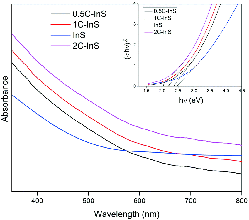 | ||
| Fig. 6 UV-vis absorbance spectra of the developed samples (Tauc plots in inset). | ||
Furthermore, the band edge potentials of the CB and VB from absolute electronegativity have been estimated from the following relation:41EVB = X − Ec + 0.5Eg and ECB = X − Ec − 0.5Eg, where X denotes the electronegativity of the constituent atoms (4.71 eV for In2S3) and Ec denotes the energy of free electrons on the hydrogen scale, which is about 4.5 eV. The calculated values are reported in Table S1, ESI.† The increasing CB edge with increasing Ce dopant concentration is well in agreement with the appearance of new atomic states in between 1 to 1.5 eV in the TDOS plots of 1C-InS, as discussed later.
The PL spectra of the synthesized samples have been recorded to assess their electron–hole recombination tendencies. An excitation wavelength of 325 nm has been used and the observed spectra are presented in Fig. 7a. All the samples exhibit emission bands centered around 460–480 nm, with the 1C-InS sample showing the least PL intensity. This is indicative of the least electron–hole recombination in the 1C-InS sample, in spite of having a narrower band gap than the pristine InS samples. This can be attributed to the intercalated Ce3+ ions acting as electron traps due to their 4f → 5d transitions, and hence, suppressing electron–hole recombination. However, excessive cerium doping has resulted in further atomic level defects acting as recombination centers, as manifested by the maximum PL response in the 2C-InS sample. This has been further validated by Gaussian deconvolution of the PL spectra of 2C-InS and 1C-InS.
 | ||
| Fig. 7 (a) PL spectra of the developed samples; (b) Gaussian deconvolution of the 1C-InS and 2C-InS PL spectra (dashed lines: original spectra, solid lines: Gaussian sum fit). | ||
The plots presented in Fig. 7b reveal 2 emission bands in the case of both 1C-InS and 2C-InS samples. The peak centered at around 460 nm can be attributed to band-to-band radiative recombination, which also results in the only peak visible in the pristine InS sample. The other peak centered at around 520 nm in the 1C-InS sample can be attributed to trapping luminescence arising from recombinations due to dopant ions. This has shown maximum intensity in the 1C-InS samples due to the successful insertion of Ce3+ ions acting as electron traps. The intensity of band-to-band excitonic luminescence in the case of the 2C-InS samples is nearly double that observed in the 1C-InS samples. Also, the trapping luminescence intensity has shown a marked reduction in 2C-InS, indicating that excess cerium ions have acted as recombination centres instead of electron trapping sites. The structural distortions due to excess cerium atoms along with its narrow band gap have resulted in maximum excitonic recombination in the 2C-InS sample. Thus, it can be concluded that the amount of cerium doping plays a major influence on the charge separation efficiency, along with controlling the morphology of the In2S3 nanoparticles.
Photoelectrochemical study
The modified electronic properties of the developed samples have been further established by measuring their transient photocurrent responses in a photoelectrochemical cell, as described earlier. From the photocurrent density plots presented in Fig. 8a, it can be clearly observed that the 1C-InS samples show a maximum photocurrent density of 0.52 mA cm−2, which is 1.15 times higher than that obtained with the pristine InS samples. The 1C-InS samples having the most optimum optical configuration as revealed by UV-vis and PL spectroscopy have achieved maximum photocurrent generation and electron–hole separation. As observed in the PDOS plots, the doped Ce atoms have resulted in the formation of new electronic states near the Fermi level of pristine In2S3, which have the ability to absorb more photons aiding in higher photocurrent generation. The Ce atoms also aid in suppressing electron–hole recombination, as established from the PL spectra. Thus, there has been good localization of charges on the smooth nanosheet surfaces. It can also be reasoned that the (200), (305) and (410) facets as observed in the 1C-InS samples have served as active sites for charge generation, resulting in higher photocurrent response than the 0.5C-InS samples. However, increasing the cerium doping percentage to 2% shows a marked reduction in photocurrent density. It can be deduced that the diffuse morphology as revealed in the SEM images, the narrow band gap as revealed in the UV-vis spectra, and the maximum electron–hole recombination as revealed in the PL spectra have impeded the localization of charges and photocurrent generation in the 2C-InS samples. | ||
| Fig. 8 (a) Transient photocurrent responses and (b) electrochemical impedance spectra (EIS) of the developed samples. | ||
The same electrochemical setup was used to obtain EIS spectra in order to evaluate the resistances to charge transfer in the developed photocatalysts. The semicircular plots observed in Fig. 8b correspond to charge transfer impedance at the electrode/electrolyte interface, with the sample exhibiting the minimum semicircular radius having the least resistance to charge transfer.42 The 1C-InS samples have shown the minimum arc radius with the arc radius increasing in the following order: 1C-InS < 0.5C-InS < InS < 2C-InS. This is well in agreement with the transient photocurrent responses, which revealed minimum photocurrent generation in the 2C-InS samples. The cerium dopants have reduced the charge transfer resistance, up to 1% doping, and upon increasing the dopant amount the charge transfer resistance showed a marked increase. Thus, the 1C-InS samples can be concluded to have the most optimum properties for photocatalytic applications. This has been validated by studying their photocatalytic activities in degradation of ciprofloxacin, as discussed later.
DFT study on geometric and electronic structures
The conventional unit cell of pristine tetragonal β-In2S3 with fully relaxed atomic coordinates is presented in Fig. 9a. The optimized lattice constants have been computed to be a = 7.61 Å and c = 32.16 Å which are very close to the experimentally obtained and reported values for tetragonal β-In2S3 belonging to the space group 141: I41/amd. As observed in Fig. 9a, the unit cell of β-In2S3 consists of layers of interlinked InS6 octahedra and InS4 tetrahedra. To realize the effect of substitutionally doped cerium atoms as revealed earlier in the TEM/XRD analyses, 1 indium atom was replaced by 1 cerium atom to obtain the cerium doped In2S3 crystal structure. Thus, a dopant concentration of 3.125% with respect to indium atoms and 1.25% with respect to all atoms in the unit cell was achieved, which can be considered reasonable enough for a comparative study with our experimentally prepared 1C-InS samples (Fig. 9b). An octahedral indium atom was replaced with a cerium atom since it is well known that dopant metals substitute octahedral indium atoms in In2S3-based compounds.43,44 Moreover, the only previous report on DFT calculations on metal ion doped tetragonal β-In2S3 revealed octahedral indium atoms to be the most energetically favorable lattice sites for metal ion substitution.45 The doped sample as presented in Fig. 9b revealed optimized lattice constant values of a = 7.64 Å and c = 36.23 Å. These are similar to the parameters obtained from the X-ray diffractograms, with the lattice constant c showing a slight increment due to the higher radius of the cerium atom.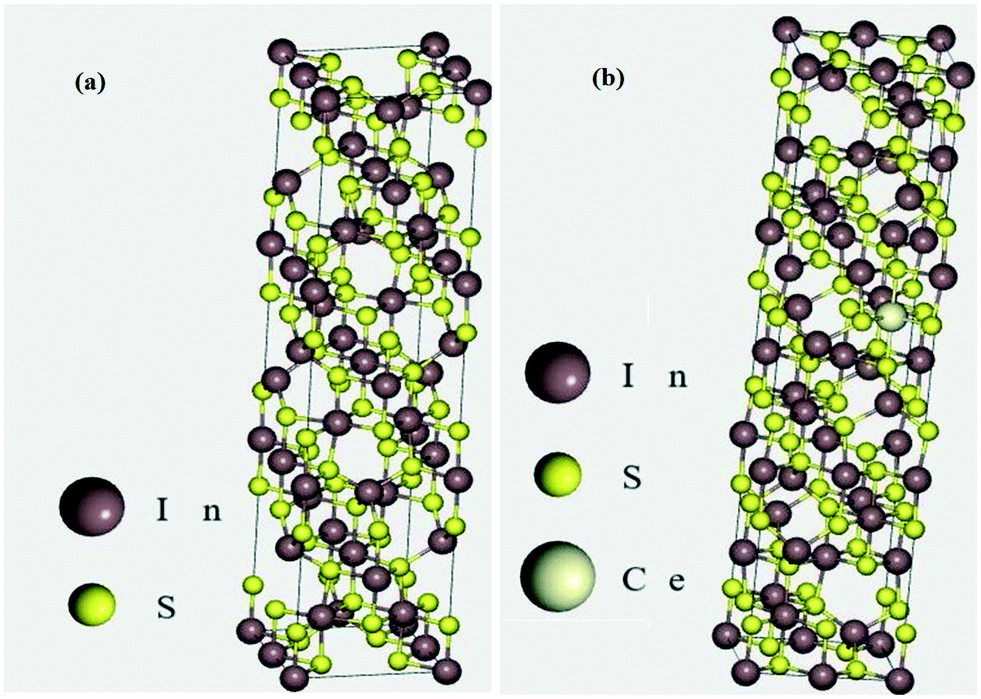 | ||
| Fig. 9 Optimized crystal geometry of (a) InS and (b) 1C-InS. | ||
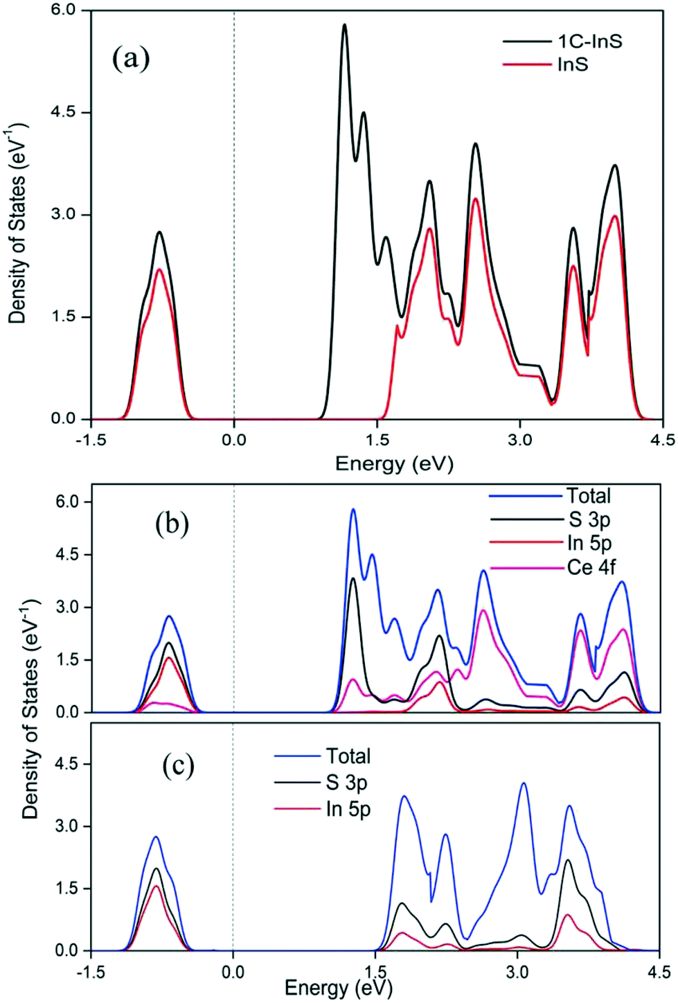
Upon obtaining the relaxed geometry, SCF convergence was performed followed by DOS calculations to theoretically determine the electronic states of the synthesized samples. The TDOS plots of InS and 1C-InS are displayed in Fig. 10a. The pristine InS reveals a band gap of almost 2 eV, which is slightly less than the experimentally obtained band gap of 2.48 eV. This slight discrepancy is due to the well-known shortcomings of DFT exchange correlations in describing electronic states. The TDOS plot of the 1C-InS samples revealed a narrowed band gap of 1.5 eV with the appearance of new atomic states very close to the Fermi level at around 1 eV. A marked increase in electron density peaks is also observed in the 1C-InS samples. This, along with the altered CB edge in the 1C-InS samples can be attributed to the presence of dopant atom cerium and hybridization of the Ce 4f and In 5p orbitals. This has been further elucidated in the PDOS plots.
 | ||
| Fig. 10 (a) TDOS plots; (b) PDOS plot of 1C-InS; (c) PDOS plot of InS. | ||
As observed in the partial density of states (PDOS) plots presented in Fig. 10b and c, the valence bands near the Fermi level in between −0.5 eV and −1.5 eV is mainly constituted of the S 3p and In 5p orbitals, with the slight presence of the Ce 4f energy states in the case of 1C-InS. Both the structures showed a broader conduction band near the Fermi level with the strong presence of the Ce 4f states in the case of 1C-InS. The hybridization of Ce 4f with the In 5p and S 3p orbitals has reduced the conduction band minimum to near 1 eV. This validates the marked reduction in the experimentally determined band gaps in the case of the doped samples. The deeper lying valence bands and conduction bands in both InS and 1C-InS also have contributions from the In 5 s and S 3s states. It can be observed that the hybridization with Ce orbitals has increased the density of states of both S 3p and In 5p orbitals in the conduction bands of the doped structures, leading to enhanced optoelectronic properties.
Photocatalytic activity
The photocatalytic properties of the developed samples were evaluated by degradation of a pharmaceutical drug ciprofloxacin in the photocatalytic reactor setup described earlier. Ciprofloxacin is a complex fluoroquinolone compound which has been earlier used as a model pollutant to test the photocatalytic potentials of novel systems like MgZnO@SiO2–tetrazine nanoparticles,46 CeO2–Ag/AgBr hybrids,47etc. However, there are no reports on In2S3-based photocatalytic degradation of ciprofloxacin.The photocatalytic performances of the prepared samples are displayed in Fig. 11. The InS/0.5C-InS/1C-InS samples have shown solid photocatalytic activity (Fig. 11a), with the 1C-InS samples achieving the best results. This can be attributed to their visible light active band gaps. The results are well in agreement with our previous analyses. The 1C-InS samples have achieved over 90% degradation in 90 minutes. The reduction of absorbance of ciprofloxacin with time during its photodegradation by 1C-InS is presented in Fig. S3, ESI.† The consistent morphology, narrow band gap, and maximum electron–hole separation of the 1C-InS samples have resulted in the maximum number of sites for photocatalytic activity. The 2C-InS samples have shown almost negligible photocatalytic activity, having degraded less than 30% in 90 minutes. This can be attributed to its maximum electron–hole recombination, as observed in the PL/EIS spectra. Thus, it can be concluded that despite its band gap narrowing, and consequent ability to absorb a greater part of the solar spectrum, doping cerium atoms into In2S3 beyond 1% is not at all suitable for photocatalysis.
 | ||
| Fig. 11 (a) Photocatalytic degradation over time; (b) degradation kinetics. | ||
From Fig. 11b, we can observe that the degradation kinetics have shown an excellent fit with pseudo first order kinetics: ln(C/C0) = −kt, which is the convention in heterogeneous photocatalysis. The rate constant values k have been computed to be 0.03 min−1, 0.02 min−1, 0.014 min−1, and 0.006 min−1 for the 1C-InS, 0.5C-InS, InS and 2C-InS samples, respectively.
Conclusion
In summary, insertion of cerium ions in the crystal lattice has a marked effect on the morphological and electronic properties of tetragonal β-In2S3 nanoparticles. The dopant concentration has been varied via a simple hydrothermal synthesis procedure to study the effects of cerium ion intercalation in the In2S3 lattice. The crystal alterations due to cerium ion incorporation have a strong effect on the morphological characteristics. As observed in the FESEM images, densely intertwined nanosheets as observed in the pristine InS samples have evolved into distinct rigid nanosheets in the 1C-InS samples. These smooth nanosheets have served as ideal sites for localization of charges, as evidenced by the maximum photocurrent generation and charge separation in the 1C-InS samples. The substitutionally doped cerium ions have also modified the optical properties of In2S3 by introducing new energy states in the band gap of pristine In2S3. The 1C-InS samples have thus shown the strongest photocatalytic activity, resulting in above 90% degradation of ciprofloxacin in visible light. However, the enhanced characteristics showed a marked deterioration upon increasing the dopant concentration to 2%. The distinct nanosheet morphology was no longer observed, owing to the limited solubility of cerium ions in the β-In2S3 lattice, and the photocatalytic activity showed a marked decline due to band gap narrowing. The excess Ce3+ ions might also serve as recombination centres, therefore hindering photocatalytic activity. The experimental results have been verified by DFT calculations by replacing an octahedral indium atom with a cerium atom in the pristine InS structures. Upon obtaining the relaxed geometry of doped structures, the DOS calculations performed revealed a downshift of the CB band edge due to hybridization of Ce 4f with the In 5p and S 3p orbitals. The narrowed band gap and the smooth electronic transitions between the Ce 4f and 5d orbitals have resulted in the capability to harness a greater part of the solar spectrum. Thus, this work demonstrates a novel approach in tuning the morphological and electronic properties of In2S3 nanoparticles by cerium ion intercalation.Conflicts of interest
There are no conflicts to declare.References
- V. Preethi and S. Kanmani, Mater. Sci. Semicond. Process., 2013, 16, 561–575 CrossRef CAS.
- M. Chong, B. Jin, C. Chow and C. Saint, Water Res., 2010, 44, 2997–3027 CrossRef CAS PubMed.
- A. Kusior, J. Kafel, A. Zajac, K. Swierczek, M. Radecka and K. Zakrzewska, J. Eur. Ceram. Soc., 2013, 33, 2285–2290 CrossRef CAS.
- K. Nakata and A. Fujishimaa, J. Photochem. Photobiol., C, 2012, 13, 169–189 CrossRef CAS.
- C. Ong, L. Ng and A. Mohammad, Renewable Sustainable Energy Rev., 2018, 81, 536–551 CrossRef CAS.
- A. Malathi, J. Madhavan, M. Ashokkumar and P. Arunachalam, Appl. Catal., A, 2018, 555, 47–74 CrossRef CAS.
- S. Rahut, S. S. Basu and J. Basu, CrystEngComm, 2019, 21, 23–29 RSC.
- T. Saison, P. Gras, N. Chemin, C. Chaneac, O. Durupthy, V. Brezova, C. Justin and J. Jolivet, J. Phys. Chem. C, 2013, 117, 22656–22666 CrossRef CAS.
- X. Hu and C. Hu, J. Solid State Chem., 2007, 117, 725–732 CrossRef.
- W. Gao, W. Liu, Y. Leng, X. Wang, X. Wang, B. Hu, D. Yu, Y. Sang and H. Liu, Appl. Catal., A, 2015, 176–177, 83–90 CrossRef CAS.
- A. Nayak, S. Lee, Y. Sohn and D. Pradhan, CrystEngComm, 2014, 16, 8064–8072 RSC.
- C. Wei, W. Guo, J. Yang, H. Fan, J. Zhang and W. Zheng, RSC Adv., 2014, 4, 50456–50463 RSC.
- S. Batabyal, S. Lu and J. Vittal, Cryst. Growth Des., 2016, 16, 2231–2238 CrossRef CAS.
- T. Tong Wu, X. Zhou, H. Zhang and X. Zhong, Nano Res., 2010, 3, 379–386 CrossRef.
- R. Diehl and R. Nitsche, J. Cryst. Growth, 1975, 28, 306–310 CrossRef CAS.
- N. Naghavi, S. Spiering, M. Powalla, B. Cavana and D. Lincot, Progr. Photovolt.: Res. Appl., 2003, 11, 437–443 CrossRef CAS.
- W. Yue, F. Wei, C. He, D. Wu, N. Tanga and Q. Qiao, RSC Adv., 2017, 7, 37578–37587 RSC.
- G. Gopinath and K. Reddy, ISRN Condens. Matter Phys., 2013, 2013, 14230–14236 CrossRef.
- S. Rengaraj, S. Venkataraj, C. Tai, Y. Kim, E. Repo and M. Sillanpaa, Langmuir, 2011, 27, 5534–5541 CrossRef CAS PubMed.
- L. Chen, Z. Zhang and W. Wang, J. Phys. Chem. C, 2008, 112, 4117–4123 CrossRef CAS.
- W. Du, J. Zhu, S. Li and X. Qian, Cryst. Growth Des., 2007, 8, 2130–2136 CrossRef.
- F. Ye, C. Cen Wang, G. Du, X. Chen, Y. Zhongb and J. Jiang, J. Mater. Chem., 2011, 21, 17063–17065 RSC.
- D. Mocatta, G. Cohen, J. Schattner, O. Millo, E. Rabani and U. Banin, Science, 2011, 77, 77–81 CrossRef PubMed.
- L. Wang, L. Xia, Y. Wu and Y. Tian, ACS Sustainable Chem. Eng., 2016, 4, 2606–2614 CrossRef CAS.
- M. Maha, M. Mohagheghi and H. Juybari, Thin Solid Films, 2013, 536, 57–62 CrossRef.
- S. Sung-Hyu Choe, T. Bang, N. Kim, H. Kim, C. Lee, M. Jin, S. Oh and W. Kim, Semicond. Sci. Technol., 2001, 16, 98–102 CrossRef.
- S. Yang, C. Xu, B. Zhang, L. Yang, S. Hua and L. Zhen, J. Colloid Interface Sci., 2017, 491, 230–237 CrossRef CAS PubMed.
- F. Li, X. Li, M. Hou, K. Cheah and W. Choy, Appl. Catal., A, 2005, 25, 181–189 Search PubMed.
- N. Yan, Z. Zhu, J. Zhang, Z. Zhao and Q. Liu, Mater. Res. Bull., 2012, 47, 1869–1873 CrossRef CAS.
- Z. Jiang, Y. Liu, T. Jing, B. Huang, X. Zhang, X. Qin, Y. Dai and M. Whangbo, J. Phys. Chem. C, 2016, 120, 2058–2063 CrossRef CAS.
- A. Monshi, M. R. Foroughi and M. R. Monshi, World J. Nano Sci. Eng., 2012, 2, 154–160 CrossRef.
- M. Mathew, R. Jayakrishnan, P. Ratheesh Kumar, C. Sudha Kartha and K. P. Vijayakumara, J. Appl. Phys., 2006, 100, 1–8 CrossRef PubMed.
- (a) J. A. Mohammed, M. Rahman and A. M. Asiri, RSC Adv., 2017, 7, 14649–14659 RSC.
- N. M. Huang, J. Nanomater., 2011, 2011, 1–6 Search PubMed.
- H. Lu, S. Wang, L. Zhao, J. Li, B. Donga and Z. Xu, J. Mater. Chem., 2011, 21, 4228–4234 RSC.
- S. Rahut, R. Panda and J. K. Basu, J. Photochem. Photobiol., A, 2017, 341, 12–19 CrossRef CAS.
- S.-H. Yu, L. Shu, Y.-S. Wu, J. Yang, Y. Xie and Y. Qian, J. Am. Chem. Soc., 1999, 82, 457–460 CAS.
- M. Afzaal, M. A. Malik and P. Brien, Chem. Commun., 2004, 334–335 RSC.
- A. I. Ekimov, A. L. Efros and A. A. Onushchenko, Solid State Commun., 1985, 56, 921–924 CrossRef CAS.
- W.-Y. Wu, J. N. Schulman, T. Y. Hsu and U. Efron, Appl. Phys. Lett., 1987, 51, 710–712 CrossRef.
- X. Lin, J. Xing, W. Wang, Z. Shan, F. Xu and F. Huang, J. Phys. Chem. C, 2007, 111, 18288–18293 CrossRef CAS.
- X. Xia, J. Tu, Y. Mai, R. Chen, X. Wang, C. Gu and X. Zhao, Chem. – Eur. J., 2011, 17, 10898–10905 CrossRef CAS PubMed.
- E. Ghorbani, P. Erhart and K. Albe, J. Mater. Chem. A, 2019, 7, 7745–7751 RSC.
- P. Palacios, I. Aguilera, K. Sanchez, J. C. Conesa and P. Wahnon, Phys. Rev. Lett., 2008, 101, 1–4 CrossRef PubMed.
- Z. Zhao, J. Yi and D. Zhou, Comput. Mater. Sci., 2013, 73, 139–145 CrossRef CAS.
- E. Parvizi, R. Tayebee, E. Koushki, M. F. Abdizadeh, B. Maleki, P. Audebertd and L. Galmiche, RSC Adv., 2019, 9, 23818–23831 RSC.
- X. Wen, C. Niu, L. Zhang, C. Liang, H. Guo and G. Zeng, J. Catal., 2018, 358, 141–154 CrossRef CAS.
Footnote |
| † Electronic supplementary information (ESI) available: Experimental section, computational methodology, Tables S1 and S2, and Fig. S1–S3. See DOI: 10.1039/d0ce00674b |
| This journal is © The Royal Society of Chemistry 2020 |