
Solution-synthesis of Sb2Se3 nanorods using KSeCN as a molecular selenium source†
Junli
Wang
 * and
Fan
Guan
* and
Fan
Guan
School of Materials Science & Engineering, Jiangsu University, Zhenjiang 212013, P. R. China. E-mail: wangjl@ujs.edu.cn; junleewang@yahoo.com
First published on 4th November 2019
Abstract
Antimony selenide (Sb2Se3) is a low-toxic, element-abundant, narrow bandgap (Eg = ∼1.1–1.3 eV) semiconductor that shows potential for UV-Visible-Near-infrared optoelectronic applications. This paper reports the use of potassium selenocyanate (KSeCN) as a novel molecular selenium source to synthesize Sb2Se3 uniform nanorods. The resulting nanorods have been carefully characterized and are found to exhibit decent photoconductivity as well as broad-spectrum optical absorption with an Eg value of ∼1.35 eV. A molecular reaction mechanism is rationally proposed and evidenced for forming Sb2Se3, which is related to the thermal decomposition of selenocyanate (SeCN−) anions through the cleaving of Se–CN bonds to elemental Se(0), followed by its reduction to Se2− anions. Our work using KSeCN offers an alternative method for the synthesis of metal selenides with desirable nanostructures and properties.
1. Introduction
Semiconductor nanowires (NWs) and nanorods (NRs) have attracted increasingly scientific and technical attention because of their promising applications in optics, electronics, optoelectronics, bioelectronics and energy-related fields.1–3 Antimony selenide (Sb2Se3) is a typical narrow bandgap (Eg = ∼1.1–1.3 eV) optoelectronic material with many attractive characteristics, such as earth-abundance and low toxicity, high optical absorption coefficient (>105 cm−1), high carrier mobility, long carrier lifetime, high photoconductivity, and decent photo and chemical stability,4,5 and therefore holds great potential as a favorable absorber or sensitizer in high-efficiency solar cells and optical detectors within the UV-visible-near-infrared (NIR) window.4–8 In recent years, a number of approaches have been exploited for the controllable preparation of Sb2Se3 films or 1D nanostructures (NWs and NRs) with the aim to obtain enhanced optoelectronic performance, generally including the physical/chemical thermal evaporation–deposition and wet chemistry methods. The thermal evaporation–deposition of thin films was often carried out with the commercially available Sb2Se3 bulk powder,5,6 which benefits from its low melting point (∼610 °C).4,6 Meanwhile, chemical vapor deposition from high purity Sb and Se powder was developed to produce high crystallinity Sb2Se3 NWs.7On the other hand, the wet chemistry routes mainly involve liquid-mediated hydrothermal/solvothermal8–14 and oil-bath reflux processes/colloidal approches.15–18 Likewise, the microwave-assisted solution synthesis,19 successive ionic layer adsorption and reaction (SILAR) method,20 electrodeposition method,21 and dissolution process in the organic amine–thiol mixture followed by recrystallization via spin-cast deposition and annealing22,23 can also be classified as wet chemistry strategies. In these methods, different kinds of selenium sources have been selected to prepare Sb2Se3 NWs/NRs or its thin films. For example, elemental Se powder, selenium dioxide (SeO2) and sodium selenite (Na2SeO3) containing zero or positively valent Se could serve as selenium sources after they are reduced to divalent Se2− anions by certain reductants, such as sodium sulfite (Na2SO3),9,21 NaBH4,10,11,20 hydrazine hydrate (N2H4·H2O)12–15 and organic amines.16,19 Other Se precursors containing Se2−, such as dibenzyldiselenide (C6H5CH2SeSeCH2C6H5),8 a single-source molecular precursor (C15H38Cl6N8OSb2Se4),17 and selenourea,18 were also reported to synthesize Sb2Se3 NWs and NRs.
Potassium selenocyanate (KSeCN) is a commercially available, inexpensive, ambient-stable reagent, and more significantly, it is a soluble salt in protic solvents and non-protic polar solvents, such as water, methanol, ethanol, DMF, DMSO, NMP, and acetonitrile.24,25 These features make KSeCN to be widely used not only in organic selenide/selenocyanate synthesis24–26 and inorganic coordination chemistry,27 but also in the wet chemistry synthesis of inorganic metal selenide compounds. In an early report, CdSe thin films could be prepared by an electrodeposition process in the aqueous solution of Cd2+ and KSeCN,28 where SeCN− is electrochemically reduced to Se2− for the generation of CdSe. Similarly, the growth of CdSe nanocrystals could be performed by immersing Cd2+-doped porous silica matrix in a solution of acidic water and KSeCN; the researchers proposed that SeCN− anions produce H2Se gas by electrophilic substitution and then react with Cd2+ ions.29 Recently, Kukunuri et al. reported the hydrothermal synthesis of NiSe hexagons by using KSeCN as a selenium source and N2H4·H2O as a reductant.30
Herein, we demonstrate for the first time, to our knowledge, the use of KSeCN as a molecular selenium source for preparing Sb2Se3 NRs through an oleylamine-mediated reflux method. The as-obtained NRs and their optoelectronic properties have been carefully characterized and evaluated. A molecular reaction mechanism involving a two-step thermolysis and reduction process from SeCN− to Se(0) and then to Se2− is proposed and substantiated for the production of Sb2Se3.
2. Experimental section
Synthesis of Sb2Se3 nanorods
All chemicals were purchased from Aladdin Chemistry Co. Ltd. (China) and were used as received without further treatments.The synthesis of Sb2Se3 nanorods is similar to the method we recently reported for Bi2S3 and Sb2S3.31 In a typical procedure, 0.5 mmol SbCl3 (0.114 g, 99.98%) and 10 ml oleylamine (OLA, 80–90%, technical grade; boiling point: 348–350 °C) were added into a 50 ml three-necked flask, and the flask was heated to 200 °C. After 20 min of magnetic stirring at 200 °C, 1 mmol KSeCN (0.144 g, 99%, solid powder) was added and the reaction continued at this temperature for 1 hour. Caution: The whole synthetic procedure was protected under an Ar flow and carried out in a fume hood, since highly harmful HCN gas may be produced. When naturally cooled to room temperature, the black Sb2Se3 products were collected by centrifugation, washed with an n-hexane/ethanol mixture (two times) and a 5![[thin space (1/6-em)]](https://www.rsc.org/images/entities/char_2009.gif) :1 (v/v) ethanol/deionized water mixture (two times) to remove organic solvents and inorganic salts, and finally dried at 60 °C. Without washing with ethanol/water, KCl would be present in the products as an inorganic salt side-product, as discussed later.
:1 (v/v) ethanol/deionized water mixture (two times) to remove organic solvents and inorganic salts, and finally dried at 60 °C. Without washing with ethanol/water, KCl would be present in the products as an inorganic salt side-product, as discussed later.
Sample characterization
Powder X-ray diffraction (XRD) was carried out on a D8 Advance diffractometer with graphite-monochromatized Cu Kα radiation (λ = 1.54178 Å, Bruker-AXS). The size and morphology of the samples were examined using a JSM-7001F scanning electron microscope (SEM). Transmission electron microscopy (TEM) and high-resolution TEM (HRTEM) images were acquired on a JEM 2100 electron microscope (working at 200 kV), attached with an energy-dispersive X-ray spectrometer (EDS) for chemical composition analysis. X-ray photoelectron spectroscopy (XPS) measurements were done on an ESCALAB250Xi X-ray photoelectron spectrometer with an Al Kα excitation source (Thermo Fisher Scientific). A Shimadzu UV-2450 spectrophotometer was used to record the UV-visible absorption spectra of the powder samples. FT-IR spectra were recorded on a Nicolet FT-170SX Fourier transform spectrometer (KBr) within the wavenumber range of 400–4000 cm−1.Photoelectric measurements
A sandwich-structured ITO/Sb2Se3/ITO device (see Fig. 3c) was made to measure the photoelectronic properties of the as-prepared Sb2Se3 NRs. The assembly details for this prototype device can be referred to our recent studies.31 A xenon lamp (300 W) with an output wavelength range of 400–780 nm was used as a light source. The monochromatic visible light of different wavelengths was separated by using optical filters (e.g., blue: 450 nm, green: 550 nm, and red: 650 nm). The light intensity was tuned by changing the distance between the xenon lamp and the device. The intensity of white light was maintained at 100 mW cm−2, while that of three kinds of visible light was 18 mW cm−2. Current–voltage (I–V) and time-dependent current (I–t) curves were recorded with a two-probe model on an electrochemical workstation (CHI660e) under ambient conditions.3. Results and discussion
Fig. 1a shows the powder X-ray diffraction (XRD) pattern of the as-prepared Sb2Se3 NRs. All of the peaks can be accurately assigned to the diffractions from Sb2Se3 crystallized in an orthorhombic crystal structure, matching well with the literature data for Sb2Se3 (JCPDS card no. 89-0821; space group: Pbnm; a = 11.58 Å, b = 11.74 Å, and c = 3.96 Å). There are no impurities detected in the XRD pattern. It was found that as long as the amount of KSeCN is higher than the 1:1.5 Sb/Se stoichiometric ratio of Sb2Se3, e.g., 1:2 and 1:3, phase-pure Sb2Se3 can be synthesized in a broad temperature range of 160–220 °C; otherwise, for example, 1:1 KSeCN:SbCl3 would result in the formation of impurities, Sb2O3 nanoparticles, besides Sb2Se3 NRs (Fig. S1, see the ESI†). The formation of Sb2O3 is caused by the hydrolysis of unreacted Sb3+ ions upon contact with a small amount of residual water in the synthesis.16b
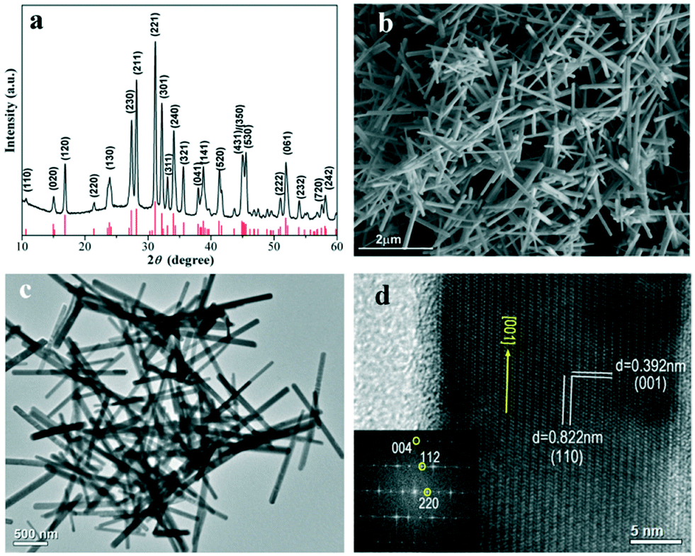 | ||
| Fig. 1 (a) XRD pattern, (b and c) SEM and TEM images, and (d) HRTEM image and FFT pattern (inset) of the Sb2Se3 NRs prepared using the 1:2 SbCl3/KSeCN precursor ratio. | ||
We will show and discuss our results for the Sb2Se3 sample prepared with a 1:2 SbCl3/KSeCN molar ratio. The scanning electron microscopy (SEM) and transmission electron microscopy (TEM) images, shown in Fig. 1b and c, clearly prove the nanorod-like morphology for the as-prepared Sb2Se3 products. Our statistical data (100 NRs) reveal the dimensional sizes of the Sb2Se3 NRs, that is, the average diameter is ∼100 nm and the length spans 1–2 micrometers. EDS elemental analysis verifies the chemical composition of ∼2:3 Sb:Se for these Sb2Se3 NRs (Fig. S1, ESI†). The crystal growth feature and lattice structure of the Sb2Se3 NRs were further investigated by high-resolution TEM (HRTEM, Fig. 1d). The result reveals the single-crystal characteristic and the favorable [001] growth direction for these NRs, which is in good agreement with the previous reports on Sb2Se3 NRs or NWs.7,8,12,13,15,19 The [001]-oriented growth habit is driven by the highly anisotropic crystal structure of orthorhombic Sb2Se3, which is composed of 1D (Sb4Se6)n ribbons as its basic building blocks. These ribbons extend along the [001] direction by the Sb–Se covalent bonds inside individual ribbons but they are linked with each other by the van der Waals attraction in the [100] and [010] crystal orientations.7,8,13 The extension of 1D (Sb4Se6)n ribbons in the [001] orientation endows Sb2Se3 NRs or NWs with the preferable [001]-grown feature.
The growth processes of the Sb2Se3 NRs were investigated by TEM characterization of the intermediate products obtained at earlier stages with short reaction times (20 and 40 min). As shown in Fig. S2,† a mixture of NRs and nanotubes were generated when the reaction duration was 20 min and they completely transformed into NRs by increasing the reaction time to 40 min. The presence of Sb2Se3 nanotubes at the early stage of the reaction was further proven by SEM studies, from which hollow cylinder-like tubes are clearly observed (Fig. S2g and h†). The production of a NR and nanotube mixture has been previously reported by Christian et al. for the octylamine-mediated synthesis of Sb2Se3 nanomaterials.16b These time-dependent experimental results suggest that NRs can be evolved from nanotubes by prolonging the reaction time.
The surface state and purity of the Sb2Se3 NRs were revealed by X-ray photoelectron spectroscopy (XPS) measurements. In the high-resolution XPS spectrum of the Sb 3d core-level, two strong major peaks with binding energies (BEs) located respectively at 528.2 and 537.6 eV (an energy split of ∼9.4 eV) are due to Sb–Se from Sb2Se3, as shown in Fig. 2a.8,11 Meanwhile, two shoulder peaks with BEs of 529.6 (3d5/2) and 539.0 eV (3d3/2), which are up-shifted by 1.4 eV relative to the two major Sb–Se peaks, can be attributed to the formation of Sb2O3 (Sb–O) at the surface.11,31 The O 1s peak, appearing at 532.2 eV, suggests the presence of surface adsorbed oxygen species (e.g., OH−, O−, and H2O),11,32 which may be removed by heating or Ar ion sputtering.33Fig. 2b shows the high-resolution Se 3d XPS spectrum, in which the BE values (Se 3d5/2: 53.5 eV and Se 3d3/2: 54.3 eV) match well with Se2− for Sb2Se3.8,11,34 The neighboring peaks with weaker intensity and a relatively high BE (3d5/2: 55.2 eV and 3d3/2: 55.9 eV) can be due to the presence of a trace amount of elemental Se(0) in the products. The BE difference and assignment in the Se(0) and Se2− 3d core-level XPS spectra are consistent with the previous reports.34,35 As revealed in the XPS survey spectrum (Fig. S3 in the ESI†), only Sb, Se, C and O elemental signals are detectable, verifying the high chemical purity of the as-prepared Sb2Se3 sample.
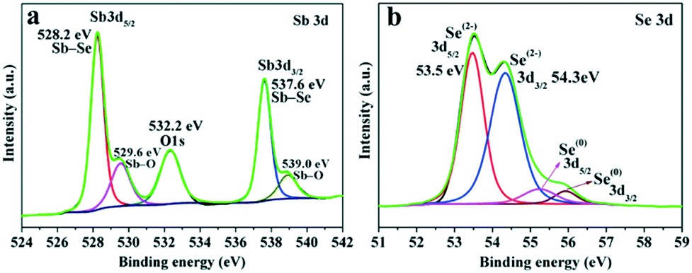 | ||
| Fig. 2 High-resolution XPS spectra of (a) Sb 3d and (b) Se 3d for the Sb2Se3 NRs. | ||
The surface oxidation and purity of the Sb2Se3 NRs could be further assessed by Raman spectroscopy (Fig. 3a). In brief, the Raman-active peak at 188 cm−1 and its relatively weak shoulder peak at 210 cm−1 are assigned to Sb2Se3,7,36 whereas those located at 188 (strong), 252 (strong), and 451 (weak) cm−1 are considered to be from surface oxide Sb2O3.7,36 A Similar Raman spectrum was also measured for the Sb2Se3 NRs that were prepared using a 1:3 SbCl3/KSeCN precursor ratio besides the same crystal structure and morphology (Fig. S4, ESI†).
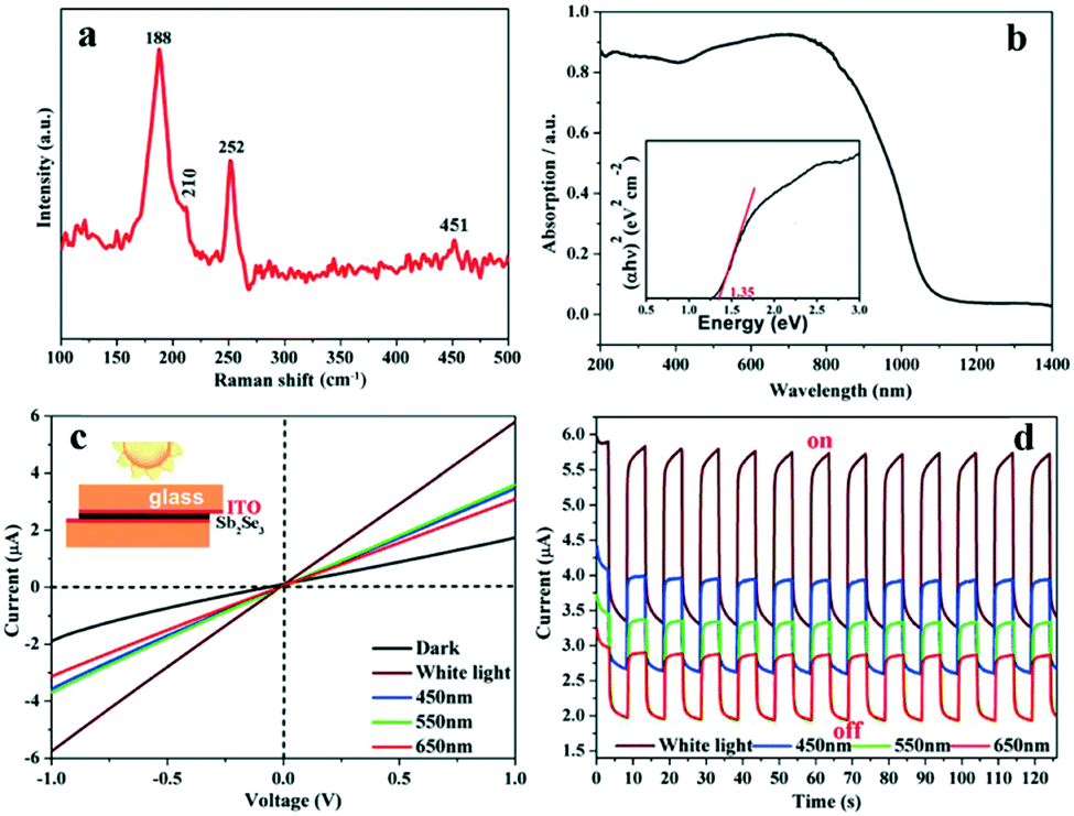 | ||
| Fig. 3 (a and b) Raman and UV-visible absorption spectra of the Sb2Se3 NRs; (c and d) I–V and I–t curves for the ITO/Sb2Se3/ITO-structured device measured under different illumination conditions. The I–t curves were recorded under 1 V. | ||
The UV-visible absorption spectrum of the Sb2Se3 NRs was recorded (Fig. 3b), from which a broad, strong absorbance peak is present in the range of 400–900 nm. Its band gap energy (Eg) can be derived to be ∼1.35 eV according to the Tauc plot of (αhν)n = B(hν − Eg) (n = 2 for a direct bandgap semiconductor; inset of Fig. 3b).7,15,18,34,37 Such an absorption nature and narrow band gap will enable the Sb2Se3 NRs as a superior optically-active material for applications in solar cells and visible-NIR photodetectors. A prototype device with an indium tin oxide (ITO)/Sb2Se3 NRs/ITO structure (inset of Fig. 3c)31 was made to investigate the photoelectronic properties of the Sb2Se3 NRs. Under irradiation with simulated sunlight (400–780 nm; 100 mW cm−2) or nearly monochromatic light of different wavelengths (e.g. blue: 450 nm, green: 550 nm, and red: 650 nm; ∼18 mW cm−2), an obviously enhanced photocurrent is detectable in the current–voltage (I–V) and time-dependent current (I–t) curves (Fig. 3c and d). This device shows good photostability during the time-dependent ON/OFF switching process as revealed by the I–t curves. Considering the surface oxidation, it is considered that the Sb2Se3 NRs can serve as an oxidation-resistant photoconductor used for optoelectronic devices, although the on/off ratio, the device structure and the quality of the Sb2Se3 film are needed to be further optimized.
Lastly, we investigate the chemical reaction process for the synthesis of Sb2Se3 from KSeCN. Firstly, as shown in reaction (1), selenocyanate (SeCN−) anions are thermally decomposed into cyanide ions (CN−) and elemental Se(0) via the cleaving of Se–CN bonds especially in the presence of reducing agents, for instance, organic amines (i.e., OLA) in this work. Similar reaction processes have been reported for the transformation of SeCN− into CN− and organic selenides24,25 or the cellular reducing process of SeCN− to elemental Se(0).38 Furthermore, it was found that KSeCN can be directly decomposed into KCN and Se(0), which is an amorphous red solid.39 The detailed analysis of the Se 3d XPS spectrum (Fig. 2b) indicates that there is a trace Se(0) impurity in the Sb2Se3 sample obtained at 1:2 SbCl3/KSeCN. As further revealed by the XPS result shown in Fig. 4a, the amount of elemental Se(0) impurity in Sb2Se3 significantly increased when a higher molar proportion of KSeCN, namely 1:10 SbCl3/KSeCN (0.1 mmol per 1 mmol), was used for the synthesis (at 220 °C for 1 h). The confirmation of the Se(0) generation supports the validity of the dissociation reaction in reaction (1).
| SeCN− → Se(0) + CN− | (1) |
| Se(0) + 2e− → Se2− | (2) |
| 3Se2− + 2Sb3+ → Sb2Se3 | (3) |
| 3KSeCH + 2SbCl3 + 6e− → Sb2Se3 + 3KCl + 3Cl− + 3CN− | (4) |
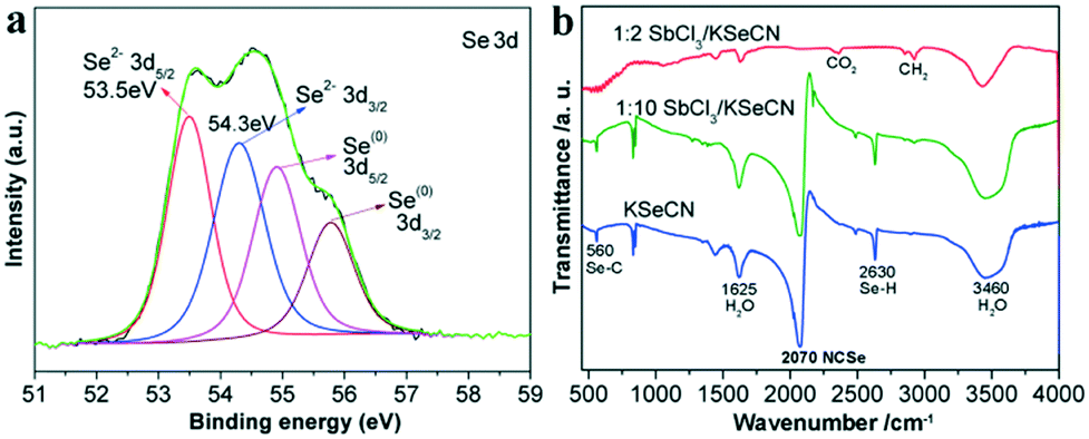 | ||
| Fig. 4 (a) Se 3d core-level XPS spectrum of the sample prepared at 1:10 SbCl3/KSeCN after washing with ethanol/water. The relative intensity of the Se(0) peaks is obviously enhanced compared to that detected for the sample prepared using 1:2 SbCl3/KSeCN shown in Fig. 2b; (b) FT-IR spectra of the dried powdered samples prepared at 1:2 and 1:10 SbCl3/KSeCN before washing with ethanol/water. IR spectrum of KSeCN is also shown for comparison. IR-active vibration bands of adsorbed H2O, CO2 and Se–H due to the adsorbed H2O are detectable in addition to selenocyanate (NCSe−, ∼2070 cm−1). | ||
The newly-yielded Se(0) can be then readily reduced to selenium anions (Se2−) through the thermal reduction process by OLA (see reaction (2)) at elevated temperatures. It is a common phenomenon that the elemental Se and S powders could be reduced to their divalent anions by octylamine, OLA or ODE (1-octadecene).16b,19,40–42 Metal cations would promote such a reduction process because of the formation of metal selenide precipitates.42 SeCN− is known as an IR-active group with a strong stretching frequency at ∼2070 cm−1 in the IR spectrum.27,39 The FT-IR spectra in Fig. 4b indicate that SeCN− exists in the Sb2Se3 sample prepared at 1:10 SbCl3/KSeCN, but not in the sample prepared at 1:2 SbCl3/KSeCN (two samples for IR studies were not washed with ethanol/water to remove the KSeCN residue for it is soluble in water). This result confirms that a suitable amount of Sb3+ can result in the complete dissociation of SeCN− to Se(0) and then to Se2− ions for the formation of Sb2Se3. Finally, an Sb2Se3 NR-like crystal grows by the cation–anion combination reaction between Sb3+ and Se2− (reaction (3)).
Overall, the whole molecular reaction mechanism for synthesizing Sb2Se3 NRs can be summarized as reaction (4). As side-products, inorganic salts and ions such as KCl, Cl− and CN− can be removed through ethanol/deionized water washing. If without this washing step, KCl will be clearly present in the Sb2Se3 NRs, which is evidenced by powder XRD studies, but KCN could not be detected (see Fig. S4a and S5, ESI†). The absence of KCN is further supported by the FT-IR spectrum (Fig. 4b, red line), in which the stretching mode due to free cyanide (CN−) at ∼2190 cm−1 (ref. 39) does not appear. At the same time, the FT-IR spectrum does not provide evidence for the existence of CN− ions in the final organic liquid reaction solvent (Fig. S6, ESI†). The concentration of CN− ions in the remaining organic solvent might be very low such that they cannot be clearly detected in the FT-IR spectrum. Another possibility is that CN− ions were discharged out with an Ar flow from the reaction flask in the form of HCN gas, which might be generated by the reaction of CN− with H+ that is released via the OLA thermolysis.40,42 Thus, it is necessary to perform the synthetic experiments in a fume hood. A highly harmful, volatile HCN gas could be collected by NaOH aqueous solution and further converted to low-toxicity substances by suitable removal methods43 or to organic amides and even carboxylic acids by hydration and hydrolysis reactions.44,45
The employment of KSeCN as a Se precursor could be extended to the preparation of Bi2Se3 nanosheets in OLA with the same reaction temperature and time (at 200 °C, 1 hour). The morphology and composition characterization results are shown in Fig. S7.† The corresponding reaction processes should follow the ones proposed for the formation of Sb2Se3 (reactions 1–4).
4. Conclusions
In summary, we successfully employed KSeCN as a novel selenium precursor for the synthesis of Sb2Se3 NRs. Their crystal phase and chemical purities, growth characteristics, and optical and optoelectronic properties were thoroughly investigated. The molecular mechanism of KSeCN precursor evolution for the synthesis was investigated and proven, which involves the release of elemental Se from selenocyanate (SeCN−) and the successive reduction to Se2− anions. Such a reaction process could be accelerated by the formation of metal selenide precipitates. As exemplified by crystalline Sb2Se3 NRs, we anticipate that more studies will be pursued and carried out that are related to the synthesis and controllable crystal growth of other inorganic metal selenides from KSeCN.Conflicts of interest
There are no conflicts to declare.Acknowledgements
This work is financially supported by the NSFC (Funding No. 21571086 and 21201086), the China Postdoctoral Science Foundation (2014M550267 and 2015T80501), and the Natural Science Foundation of Jiangsu Province (BK20141297).Notes and references
- F. D. Wang, A. G. Dong and W. E. Buhro, Chem. Rev., 2016, 116, 10888–10933 CrossRef CAS PubMed.
- R. Yan, D. Gargas and P. Yang, Nat. Photonics, 2009, 3, 569–576 CrossRef CAS.
- W. Zhou, X. Dai and C. M. Lieber, Rep. Prog. Phys., 2017, 80, 016701 CrossRef PubMed.
- X. M. Wang, R. F. Tang, C. Y. Wu, C. F. Zhu and T. Chen, J. Energy Chem., 2018, 27, 713–721 CrossRef.
- X. X. Wen, C. Chen, S. C. Lu, K. H. Li, R. Kondrotas, Y. Zhao, W. H. Chen, L. Gao, C. Wang, J. Zhang, G. D. Niu and J. Tang, Nat. Commun., 2018, 9, 2179 CrossRef.
- Y. Zhou, L. Wang, S. Y. Chen, S. K. Qin, X. S. Liu, J. Chen, D.-J. Xue, M. Luo, Y. Z. Cao, Y. B. Cheng, E. H. Sargent and J. Tang, Nat. Photonics, 2015, 9, 409–415 CrossRef CAS.
- Z. P. Ma, S. N. Chai, Q. L. Feng, L. Li, X. B. Li, L. L. Huang, D. Y. Liu, J. Sun, R. B. Jiang, T. Y. Zhai and H. Xu, Small, 2019, 15, 1805307 CrossRef.
- G. H. Chen, W. L. Wang, C. D. Wang, T. Ding and Q. Yang, Adv. Sci., 2015, 2, 1500109 CrossRef PubMed.
- D. B. Wang, D. B. Yu, M. W. Shao, W. C. Yu and Y. T. Qian, Chem. Lett., 2002, 1056–1057 CrossRef CAS.
- T. Y. Zhai, M. F. Ye, L. Li, X. S. Fang, M. Y. Liao, Y. F. Li, Y. S. Koide, Y. S. Bando and D. T. Golberg, Adv. Mater., 2010, 22, 4530–4533 CrossRef CAS.
- X. Ou, C. H. Yang, X. H. Xiong, F. H. Zheng, Q. C. Pan, C. Jin, M. L. Lin and K. Huang, Adv. Funct. Mater., 2017, 27, 1606242 CrossRef.
- J. M. Ma, Y. P. Wang, Y. J. Wang, P. Peng, J. B. Lian, X. C. Duan, Z. F. Liu, X. D. Liu, Q. Chen, T. Kim, G. Yao and W. J. Zheng, CrystEngComm, 2011, 13, 2369–2374 RSC.
- J. M. Ma, Y. P. Wang, Y. J. Wang, Q. Chen, J. B. Lian and W. J. Zheng, J. Phys. Chem. C, 2009, 113, 13588–13592 CrossRef CAS.
- Y. Liang, Y. Y. Wang, J. N. Wang, S. M. Wu, D. Y. Jiang and J. B. Lian, RSC Adv., 2016, 6, 11501–11506 RSC.
- M. J. Wang, W. Wu, X. R. Zheng, X. Hou, C. C. Liu, Q. Y. Hao and H. Liu, Mater. Lett., 2017, 193, 191–194 CrossRef CAS.
- (a) Y. K. Liu, Y. Q. Tang, Y. Zeng, X. Luo, J. Y. Ran, Y. M. Luo, X. D. Su, B. K. Ng, F. Y. Liu and L. X. Jiang, RSC Adv., 2017, 7, 24589–24593 RSC; (b) P. Christian and P. O'Brien, J. Mater. Chem., 2005, 15, 4949–4954 RSC.
- N. Maiti, S. H. Im, Y. H. Lee, C. H. Kim and S. I. Seok, CrystEngComm, 2011, 13, 3767–3772 RSC.
- (a) A. K. Guria, G. Prusty, S. Chacrabarty and N. Pradhan, Adv. Mater., 2016, 28, 447–453 CrossRef CAS PubMed; (b) A. Y. Koposov, CrystEngComm, 2017, 19, 3098–3102 RSC.
- Y.-Q. Liu, M. Zhang, F.-X. Wang and G.-B. Pan, J. Mater. Chem. C, 2014, 2, 240–244 RSC.
- N. Guijarro, T. Lutz, T. L. Villarreal, F. O'Mahony, R. Gómez and S. A. Haque, J. Phys. Chem. Lett., 2012, 3, 1351–1356 CrossRef CAS.
- T. T. Ngo, S. Chavhan, I. Kosta, O. Miguel, H. J. Grande and R. Tena-Zaera, ACS Appl. Mater. Interfaces, 2014, 6, 2836–2841 CrossRef CAS PubMed.
- D. H. Webber and R. L. Brutchey, J. Am. Chem. Soc., 2013, 135, 15722–15725 CrossRef CAS.
- M. R. Hasan, E. S. Arinze, A. K. Singh, V. P. Oleshko, S. Q. Guo, A. Rani, Y. Cheng, I. Kalish, M. E. Zaghloul, M. V. Rao, N. V. Nguyen, A. Motayed, A. V. Davydov, S. M. Thon and R. Debnath, Adv. Electron. Mater., 2016, 2, 1600182 CrossRef.
- A. A. Heredia, Synlett, 2014, 25, 748–749 CrossRef CAS.
- A. V. Kumar, V. P. Reddy, C. S. Reddy and K. R. Rao, Tetrahedron Lett., 2011, 52, 3978–3981 CrossRef CAS.
- J. C. Guillemin, Curr. Org. Chem., 2011, 15, 1670–1687 CrossRef CAS.
- J. L. Burmeister and M. Y. Al-Janabi, Inorg. Chem., 1965, 4, 962–965 CrossRef CAS.
- M. Skyllas-Kazacos, J. Electroanal. Chem. Interfacial Electrochem., 1983, 148, 233–239 CrossRef CAS.
- D. C. Hummel, I. L. Torriani, A. Y. Ramos, A. F. Craievich, N. De La Rosa-Fox and L. Esquivias, Mater. Res. Soc. Symp. Proc., 1994, 346, 673–678 CrossRef CAS.
- S. Kukunuri, M. R. Krishnana and S. Sampath, Phys. Chem. Chem. Phys., 2015, 17, 23448–23459 RSC.
- J. L. Wang, H. S. Yu, T. T. Wang, Y. J. Qiao, Y. Feng and K. M. Chen, ACS Appl. Mater. Interfaces, 2018, 10, 7334–7343 CrossRef CAS.
- N. A. Merino, B. P. Barbero, P. Eloy and L. E. Cadús, Appl. Surf. Sci., 2006, 253, 1489–1493 CrossRef CAS.
- X. S. Liu, J. Chen, M. Luo, M. Y. Leng, Z. Xia, Y. Zhou, S. K. Qin, D.-J. Xue, L. Lv, H. Huang, D. M. Niu and J. Tang, ACS Appl. Mater. Interfaces, 2014, 6, 10687–10695 CrossRef CAS.
- C. Chen, Y. Zhao, S. Lu, K. Li, Y. Li, B. Yang, W. Chen, L. Wang, D. Li, H. Deng, F. Yi and J. Tang, Adv. Energy Mater., 2017, 7, 1700866 CrossRef.
- Z.-L. Liu, X. Wu, Y. Shao, J. Qi, Y. Cao, L. Huang, C. Liu, J.-O. Wang, Q. Zheng, Z.-L. Zhu, K. Ibrahim, Y.-L. Wang and H.-J. Gao, Sci. Bull., 2018, 63, 419–425 CrossRef CAS.
- A. Shongalova, M. R. Correia, B. Vermang, J. M. V. Cunha, P. M. P. Salomé and P. A. Fernandes, MRS Commun., 2018, 8, 865–870 CrossRef CAS.
- H. Yu, J. L. Wang, T. T. Wang, H. S. Yu, J. Yang, G. W. Liu, G. J. Qiao, Q. Yang and X. N. Cheng, CrystEngComm, 2017, 19, 727–733 RSC.
- R. A. Montes, G. A. Pradenas, J. M. Pérez-Donoso, C. C. Vásquez and T. G. Chasteen, Environ. Biotechnol., 2012, 8, 32–38 Search PubMed.
- J. S. Thayer, J. Organomet. Chem., 1967, 9, P30–P32 CrossRef CAS.
- J. W. Thomson, K. Nagashima, P. M. Macdonald and G. A. Ozin, J. Am. Chem. Soc., 2011, 133, 5036–5041 CrossRef CAS PubMed.
- J. Joo, H. B. Na, T. Yu, J. H. Yu, Y. W. Kim, F. Wu, J. Z. Zhang and T. Hyeon, J. Am. Chem. Soc., 2003, 125, 11100–11105 CrossRef CAS.
- C. Pu, J. Zhou, R. Lai, Y. Niu, W. Nan and X. Peng, Nano Res., 2013, 6, 652–670 CrossRef CAS.
- B. Han, Z. Shen and S. R. Wickramasinghe, J. Membr. Sci., 2005, 257, 171–181 CrossRef CAS.
- X.-Y. Ma, Y. He, Y.-L. Hu and M. Lu, Tetrahedron Lett., 2012, 53, 449–452 CrossRef CAS.
- R. G. Álvarez, P. Crochet and V. Cadierno, Green Chem., 2013, 15, 46–66 RSC.
Footnote |
| † Electronic supplementary information (ESI) available: Fig. S1–S7: TEM and SEM images, EDS and Raman spectra, XPS survey spectra, and XRD patterns of the Sb2Se3 samples prepared using different Sb/Se precursor ratios or at earlier reaction stages; FT-IR spectrum of liquid solution obtained after material synthesis; TEM and EDS results of Bi2Se3 nanosheets. See DOI: 10.1039/c9ce01399g |
| This journal is © The Royal Society of Chemistry 2020 |