
Organic single crystals of cyano-substituted p-phenylene vinylene derivatives as transistors with low surface trap density†
Jian
Deng‡
 ,
Yuejuan
Wan‡
,
Chang
Cai
,
Cheng
Gu
* and
Yuguang
Ma
*
,
Yuejuan
Wan‡
,
Chang
Cai
,
Cheng
Gu
* and
Yuguang
Ma
*
State Key Laboratory of Luminescent Materials and Devices, Institute of Polymer Optoelectronic Materials and Devices, South China University of Technology, No. 381 Wushan Road, Tianhe, Guangzhou 510640, P. R. China. E-mail: gucheng@scut.edu.cn; ygma@scut.edu.cn
First published on 14th October 2020
Abstract
We obtained two high-quality lamellar crystals of cayno-substituted p-phenylene vinylene derivatives and fabricated their transistors. The transistors demonstrated hysteresis-free, low subthreshold swing values of 0.15 and 0.10 V dec−1, and high mobilities of 0.56 and 2.73 cm2 V−1 s−1, respectively. More importantly, the low defect density of 1 per 9.22 × 10³ and 1.82 × 10⁴ molecules, respectively, confirmed their high crystal quality.
Organic Field-effect transistors (OFETs) featuring flexibility and switch function1,2 are very important for next-generation logical circuits. Though there are many studies on OFETs demonstrating higher mobility than polycrystalline silicon, the hysteresis and subthreshold swing (S),3,4 which determine the response speed of transistors, are still significantly larger than those of inorganic transistors (Table S6, ESI†). There is still a lack of systematic studies and efficient methods to reduce the S of OFETs. High trap density in organic semiconductors limits the further reduction of S and improves their corresponding response speed.5 Organic crystals featuring low impurity and clear structural information are convenient for the quantitative study of the structure–property relationship and development of high-performance devices.6–8 OFETs demand lamellar crystals for efficient carrier injections,9–11 whereas the shapes of most organic crystals are bulk and very difficult to control.
Herein, we report two organic lamellar crystals, shapes of which guaranteed enough electric field for efficient charge injection, featuring low trap density (TD) in the crystal, fast response speed and hysteresis-free OFETs. The crystals were constructed by combining π–π interactions and intermolecular hydrogen bonds in orthogonal directions, whereas there were only weak van der Waals forces in the third direction. The stronger interactions dominated the growth directions during the crystallisation and resulted in lamellar crystals, which was verified in our previous studies. OFETs based on the lamellar crystals were fabricated, then their device performances were optimised by the modification of the dielectric layer, resulting in high-performance transistors with mobilities up to 0.56 and 2.73 cm2 V−1 s−1 for the two crystals, respectively. The I–V curves were carefully analysed, and the resulting trap densities of less than 1.02 × 10¹⁰ and 4.64 × 1010 cm−2 quantificationally showed high quality of our two organic crystals, respectively.
The cyano-substituted oligo(p-phenylene vinylene) (CN-OPV) derivatives, namely (2Z,2′Z)-2,2′-(1,4-phenylene)bis(3-(thiophen-3-yl)acrylonitrile) (α-PBTA) and (2Z,2′Z)-3,3′-(benzo[1,2-b:5,4-b′]dithiophene-2,6-diyl)bis(2-(thiophen-3-yl)acrylonitrile) (β-DBPA) were synthesised by Knoevenagel reaction12 (ESI,† and Fig. S1–S10). Their high-quality lamellar crystal forms were obtained by carefully optimising growth conditions during the physical vapor transport (PVT) method13 (Fig. S11 and Tables S1, S2, ESI†), resulting in crystals with sizes up to several hundreds of micrometres and thickness no more than several hundreds of nanometres. The crystals showed no boundaries and cracks under UV irradiation, appearing to be of very high quality. The crystal structures were obtained from single crystal XRD experiments. The crystals of α-PBTA showed a triclinic lattice with the space group P![[1 with combining macron]](https://www.rsc.org/images/entities/char_0031_0304.gif) and cell parameters of a = 3.9383(8) Å, b = 5.8698(12) Å, c = 18.065(4) Å, α = 80.840(3), β = 87.250(3)°, γ = 86.08(3)° (Fig. S12a, b and Table S2, ESI†). The molecules stack into lattice columns through π–π interaction along the [110] direction one on top of the other with the slip angle of 84.90° along the long molecule axis (Fig. 1b), and the distance between the adjoining π-plane is 3.499 Å. The multiple hydrogen bonds interconnect the adjacent molecules with each other within the molecular plane to form the layer-like molecule packing (Fig. 1a). Furthermore, the layer-by-layer structure with uniaxially orientated stacking between adjacent layers formed, as shown in Fig. 1b. The molecules showed a very small twisted angle along with its molecular skeleton (8.173° and 2.574°, Fig. 1c). The crystal density was 1.392 g cm−3. On the other hand, the crystals of β-DBPA showed a monoclinic lattice with the space group of P21 and cell parameters of a = 3.9035(4) Å, b = 44.025(6) Å, c = 6.0394(6) Å, α = γ = 90°, β = 95.691° (Fig. S12c, d and Table S2, ESI†). The molecules stack into lattice columns through the π–π interaction along an a-axis one on top of the other with the slip angle of 72.04° along the long molecule axis (Fig. 1d), and the distance between the adjoining π–plane is 3.493 Å. The multiple hydrogen bonds interconnect the adjacent molecules with each other along the [101] direction to form the layer-like molecular packing (Fig. 1c). Furthermore, a layer-by-layer structure with herringbone stacking between the adjacent layers formed, as shown in Fig. S12d (ESI†). The molecules showed a very small twisted angle along with its molecular skeleton (1.100° and 6.714°, Fig. 1c). The closer molecular stacking resulted in a higher crystal density of 1.430 g cm−3, together with the typical H-type aggregation and the smaller twisted skeleton were superior to charge migrations, which was compatible with the fabrication of high-performance OFETs.
and cell parameters of a = 3.9383(8) Å, b = 5.8698(12) Å, c = 18.065(4) Å, α = 80.840(3), β = 87.250(3)°, γ = 86.08(3)° (Fig. S12a, b and Table S2, ESI†). The molecules stack into lattice columns through π–π interaction along the [110] direction one on top of the other with the slip angle of 84.90° along the long molecule axis (Fig. 1b), and the distance between the adjoining π-plane is 3.499 Å. The multiple hydrogen bonds interconnect the adjacent molecules with each other within the molecular plane to form the layer-like molecule packing (Fig. 1a). Furthermore, the layer-by-layer structure with uniaxially orientated stacking between adjacent layers formed, as shown in Fig. 1b. The molecules showed a very small twisted angle along with its molecular skeleton (8.173° and 2.574°, Fig. 1c). The crystal density was 1.392 g cm−3. On the other hand, the crystals of β-DBPA showed a monoclinic lattice with the space group of P21 and cell parameters of a = 3.9035(4) Å, b = 44.025(6) Å, c = 6.0394(6) Å, α = γ = 90°, β = 95.691° (Fig. S12c, d and Table S2, ESI†). The molecules stack into lattice columns through the π–π interaction along an a-axis one on top of the other with the slip angle of 72.04° along the long molecule axis (Fig. 1d), and the distance between the adjoining π–plane is 3.493 Å. The multiple hydrogen bonds interconnect the adjacent molecules with each other along the [101] direction to form the layer-like molecular packing (Fig. 1c). Furthermore, a layer-by-layer structure with herringbone stacking between the adjacent layers formed, as shown in Fig. S12d (ESI†). The molecules showed a very small twisted angle along with its molecular skeleton (1.100° and 6.714°, Fig. 1c). The closer molecular stacking resulted in a higher crystal density of 1.430 g cm−3, together with the typical H-type aggregation and the smaller twisted skeleton were superior to charge migrations, which was compatible with the fabrication of high-performance OFETs.
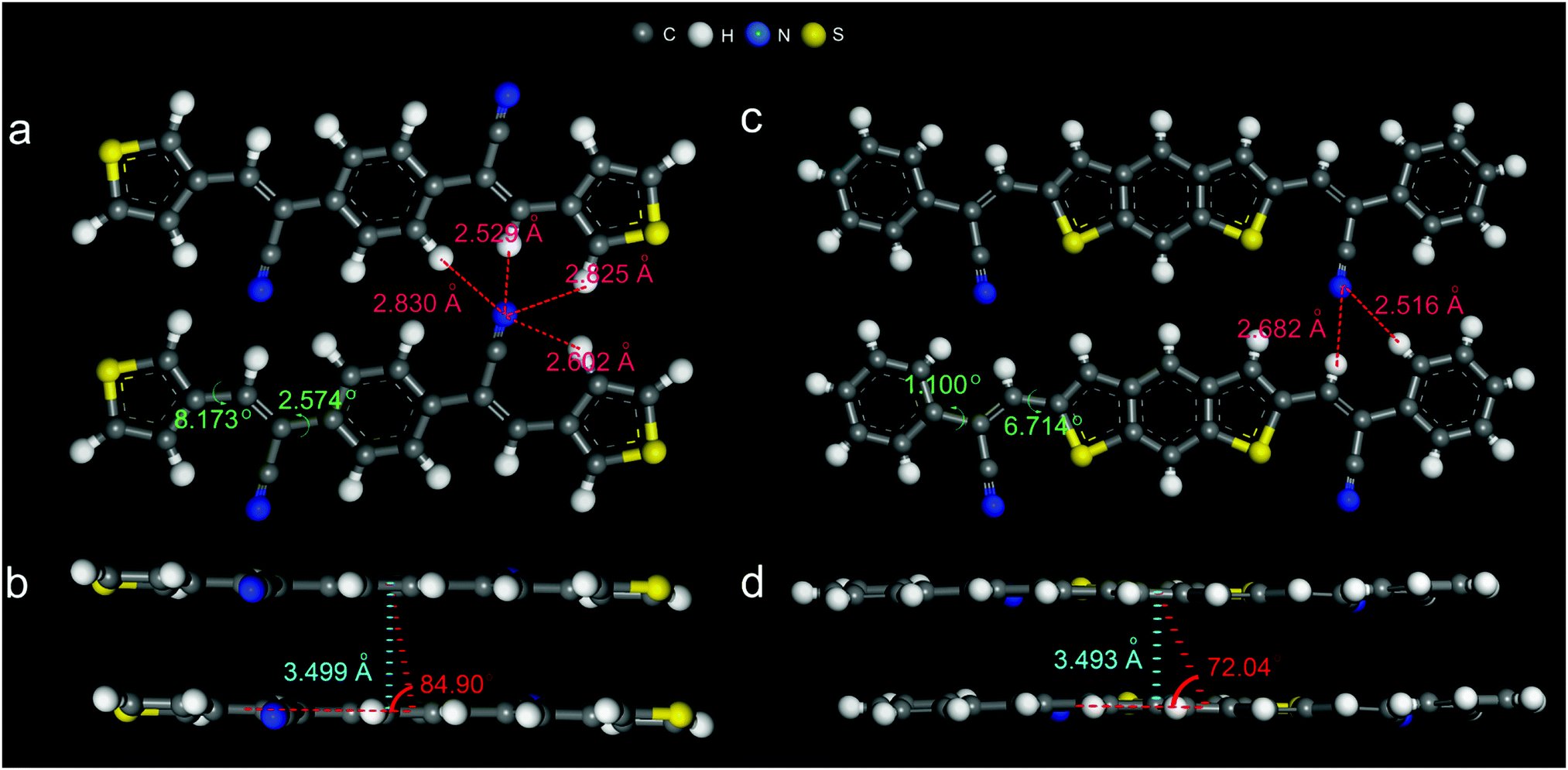 | ||
| Fig. 1 (a) The length of the hydrogen bonds (red color) and the molecular twisted angle (green color) in the crystal of α-PBTA. (b) The π–π distance (red color) and the slipping angle (sky-blue color) in the crystal of α-PBTA. (c) The length of the hydrogen bonds (red color) and the molecular twisted angle (green color) in the crystal of β-DBPA. (d) The π–π distance (red color) and the slipping angle (sky-blue color) in the crystal of β-DBPA. | ||
With the obtained lamellar crystals, OFETs were fabricated with PMMA14 as the initial buffer layer on the silicon dioxide (SiO2) dielectric layer since it is the most commonly utilised and usually brings considerable performance. All the OFETs were applied bottom gate/top contact (BG/TC) configuration to promote crystal/electrode contacts. At the very beginning, calcium and gold were respectively employed as the source and drain electrodes to form asymmetric OFETs (Fig. S17a, ESI†) and evaluated if there were any ambipolar characteristics. It turned out that all the transistors demonstrated only typical P-type unipolar I–V curves. Then, symmetric OFETs with gold electrodes (Fig. S13b, ESI†) were fabricated. The I–V curves of OFETs based on α-PBTA exhibited an obvious nonlinear increase in the initial part of the output curves (Fig. 2a, dashed lines), which was a typical feature of the Schottky contact with obvious injection barriers.5 When the applied gate voltage (Vg) was −80 V, the maximum current density (Jout,max) of 0.201 kA cm−2 was estimated with the measured maximum output drain current (Id) of 1.73 μA, and the channel width of 850 μm as well as the channel thickness of 1 nm. The carrier mobility of 0.11 cm2 V−1 s−1 and the threshold voltage of −28.77 V were extracted from the saturation region of transfer curves (Fig. 2b, dash line). Its minimum S in transfer curves was 1.5 V dec−1, from which the TD of 1.81 × 1012 cm−2 in the crystal/dielectric buffer layer interface was extracted according to Nt = [S![[thin space (1/6-em)]](https://www.rsc.org/images/entities/i_char_2009.gif) log(e)/(kT/q) − 1]Ci/q,11 and the method is described in detail in the ESI.† Moreover, the I–V curves of OFETs based on the lamellar crystal of β-DBPA also exhibit an obvious nonlinear increase in the initial part of output curves (Fig. 2c, dashed lines). The Id was kept less than 1 nA until the drain voltage (Vd) was higher than −10 V. The maximum Id was 7.05 μA when the Vg was only −60 V. Its Jout,max reached 11.2 kA cm−2 according to the channel width of 63.3 μm. The carrier mobility of 1.71 cm2 V−1 s−1 and the threshold voltage of −20.83 V were calculated from the saturation region of transfer curves (Fig. 2d, dashed lines). The obtained minimum S was 0.75 V dec−1, by which the minimum defect density in the interface of 8.69 × 1011 cm−2 was estimated. A smaller hysteresis of the transfer curve was observed in the OFETs when Vg was swept forward and backward, with the on/off ratio (Ion/off) higher than 106, as illustrated in detail in Table S4 (ESI†).
log(e)/(kT/q) − 1]Ci/q,11 and the method is described in detail in the ESI.† Moreover, the I–V curves of OFETs based on the lamellar crystal of β-DBPA also exhibit an obvious nonlinear increase in the initial part of output curves (Fig. 2c, dashed lines). The Id was kept less than 1 nA until the drain voltage (Vd) was higher than −10 V. The maximum Id was 7.05 μA when the Vg was only −60 V. Its Jout,max reached 11.2 kA cm−2 according to the channel width of 63.3 μm. The carrier mobility of 1.71 cm2 V−1 s−1 and the threshold voltage of −20.83 V were calculated from the saturation region of transfer curves (Fig. 2d, dashed lines). The obtained minimum S was 0.75 V dec−1, by which the minimum defect density in the interface of 8.69 × 1011 cm−2 was estimated. A smaller hysteresis of the transfer curve was observed in the OFETs when Vg was swept forward and backward, with the on/off ratio (Ion/off) higher than 106, as illustrated in detail in Table S4 (ESI†).
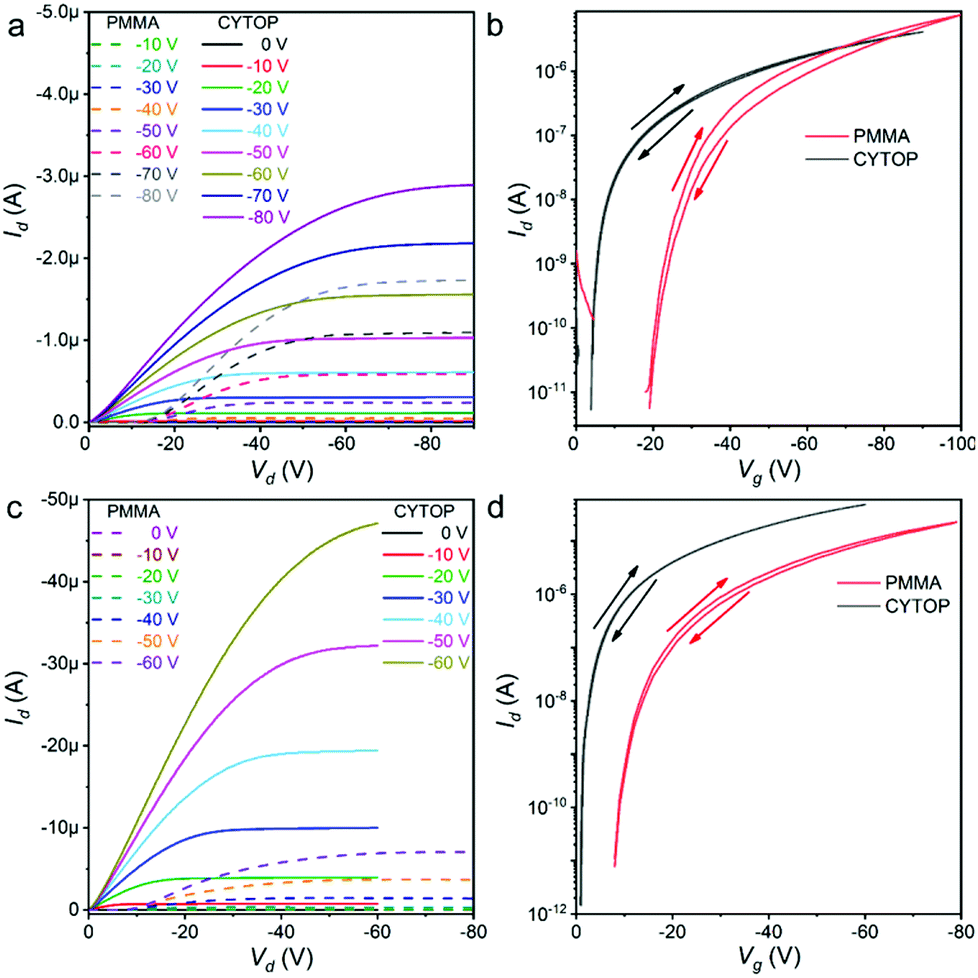 | ||
| Fig. 2 (a) Output curves of OFETs based on the single crystal of α-PBTA. The dashed curves were the I–V curves from OFETs with the PMMA buffer layer, while the solid curves were the I–V curves from OFETs with the CYTOP buffer layer. (b) Transfer characteristics of the transistors based on the single crystals of α-PBTA. In the transfer characteristics, Vd = −110 and −80 V for OFETs with (red line) PMMA and (black line) CYTOP buffer layers, respectively. (c) Output curves of OFETs are based on the single crystal of β-DBPA. The dash curves were the I–V curves from OFETs with the PMMA buffer layer, while the solid curves were the I–V curves from OFETs with the CYTOP buffer layer. (d) Transfer characteristics of the transistors based on the single crystals of β-DBPA. In the transfer characteristics, Vd = −80 and −60 V for OFETs with (red line) PMMA and (black line) CYTOP buffer layers, respectively. The transfer curves were swept forward and backward to evaluate their hysteresis. | ||
To reduce the injection barrier and improve the device performance, perfluoro(1-butenylvinylether)polymer (CYTOP)15 was utilised as a buffer layer instead of PMMA (Fig. S17c, ESI†). The devices were fabricated under otherwise identical conditions. OFETs based on two lamellar crystals demonstrated much superior performances. In the transistors of α-PBTA, the drain current (Id) almost linearly increased along with the increase in Vd (Fig. 2a, solid lines), indicating the resistance between the crystal and gold electrodes was almost negligible. The Jout,max of 7.61 kA cm−2 was estimated when Vg = −60 V with the measured maximum Id (2.89 μA) and the channel width of 38.0 μm. The minimum S in the transfer curves decreased to 0.15 V dec−1 (Fig. 2b, solid lines), which was reduced ten-folds compared with that in the OFETs with PMMA as the buffer layer. The extracted defect density in the interface was only 1.02 × 1011 cm−2. The hysteresis of transfer curves was only 0.8 V when Vg was swept forward and backward. The improvements in the transistors of β-DBPA were quite similar. In the output curves (Fig. 2c, solid lines), the Id increased linearly with the Vd in the initiation region, and the intercept between the Y-axis and Id of the linear region came across the original point, indicating that the interface of the crystal and electrodes became Ohmic contact. The output current at a high voltage was limited by the space-charge-limited current (SCLC). The maximum Id in the transistors reached 47.3 μA when the Vg was only −60 V, and the Jout,max was 58.5 kA cm−2 in the device with a channel width of 80.9 μm. The resulting maximum current density was 4.22 times higher than that in the transistors with the PMMA buffer layer under the same Vg (Table S4, ESI†). From the transfer curves (Fig. 2d, solid lines), the threshold voltage decreased to −3.60 V. The minimum S decreased from 0.75 V dec−1 to 0.10 V dec−1. The extracted TD in the interface was 4.64 × 1010 cm−2, which was one of the transistors with the lowest S and TD (Table 1), as obtained by OFETs. With the lattice parameters, we could quantitatively know the quality of the crystals; the calculation method is listed in the ESI,† (calculation of defects in organic crystals) and eqn (S4) and (S5) (ESI†). The molecule densities of α-PBTA and β-DBPA in the carrier migration plane were 9.40 × 10¹⁴ and 8.43 × 1014 cm−2, respectively. Thus, the resulting deep-TD was less than 1 per 9.22 × 10³ and 1.82 × 10⁴ molecules in the crystal of α-PBTA and β-DBPA, respectively. To the best of our knowledge, only rubrene crystals with a careful treatment achieved better quality,30 indicating the outstanding quality of our crystals. The carrier mobility was derived from the transfer curves in the saturation region, which were dependent on the variation of Vg, which ensured the accuracy of the calculated carrier mobility. The highest hole mobilities of α-PBTA and β-DBPA were 0.56 and 2.73 cm2 V−1 s−1, respectively (Table S4, ESI†). According to the crystal structure analyses, β-DBPA had a closer and larger π–π overlap, which increases the overlap integral and improves the carrier mobility.32 Moreover, β-DBPA had stronger interactions between adjacent molecules, which were critical to decrease the TD of crystal33 and further improve the device performance.
| Organic semiconductors | S (V dec−1) | TD (× 1012 cm−2) | Ref. |
|---|---|---|---|
–![[thin space (1/6-em)]](https://www.rsc.org/images/entities/char_2009.gif) Not mentioned, and could not be calculated due to lack of necessary data. Not mentioned, and could not be calculated due to lack of necessary data. |
|||
| C8-BTBT/F4-TCNQ | 1.1 | 2.34 | 16 |
| C8-BTBT/SiO2 | 0.480 | 2.90 | 17 |
| C8-BTBT/HfO2 | 0.145 | 5.12 | |
| Dinaphtho[2,3-b:2′,3′-f]thieno[3,2-b]thiophene | 0.079 | — | 18 |
| P3HT | 14 | 0.23 | 19 |
| C12-BTBT/F4-TCNQ | 0.3 | — | 20 |
| CuPc | 0.69 | 0.241 | 21 |
| C10-DNBDT | 0.25 | 0.69 | 22 |
| C16IDT-BT | 2.1 | 0.85 | 23 |
| PTCDI-Br2-C18 | 0.270 | 0.596 | 24 |
| PDIF-CN2 | 0.45 | 2.0 | 25 |
| Pentacene | 0.080 | 0.11 | 26 |
| Cy-NDI | 2.2 | — | 27 |
| DMDCNQI | 1.3 | — | |
| PTVTF | 1.7 | — | 28 |
| C10-DNBDT crystal | 0.4 | 0.22 | 29 |
| Rubrene crystal | 0.065 | 0.0030 | 30 |
| Pentacene crystal | 0.3 | 0.11 | 31 |
| α-PBTA crystal | 0.15 | 0.102 | This work |
| β-DBPA crystal | 0.10 | 0.046 | |
In conclusion, the integration of multiple intermolecular hydrogen bonds and π–π interactions during crystal engineering was critical to develop high quality lamellar organic single crystals compatible with the device fabrication. Closer intermolecular packing brings stronger intermolecular forces, reduce the trap density from 1.02 × 1011 cm−2 in the crystal of α-PBTA to 4.64 × 1010 cm−2 and in β-DBPA, improves the carrier mobility from 0.56 cm2 V−1 s−1 to 2.73 cm2 V−1 s−1, resulting in faster on/off switch speed in the transistors of β-DBPA. This work demonstrated a method to study the structure–property relationship quantificationally and an efficient way to obtain high-quality organic crystals for high-performance OFETs.
This work was supported by the National Natural Science Foundation of China (No. 91833304, 21975078 and 51703065), the Introduced Innovative R&D Team of Guangdong Province (201101C0105067115), the Natural Science Foundation of Guangdong Province (2019B030301003), the 111 Project, the Fundamental Research Funds for the Central Universities, and the Thousand Youth Talents Plan.
Conflicts of interest
There are no conflicts to declare.Notes and references
- T. Someya, T. Sekitani, S. Iba, Y. Kato, H. Kawaguchi and T. Sakurai, Proc. Natl. Acad. Sci. U. S. A., 2004, 101, 9966–9970 CrossRef CAS.
- T. Sekitani, S. Iba, Y. Kato, Y. Noguchi, T. Someya and T. Sakurai, Appl. Phys. Lett., 2005, 87, 173502 CrossRef.
- K. P. Pernstich, S. Haas, D. Oberhoff, C. Goldmann, D. J. Gundlach, B. Batlogg, A. N. Rashid and G. Schitter, J. Appl. Phys., 2004, 96, 6431–6438 CrossRef CAS.
- J. K. Jeong, J. H. Jeong, H. W. Yang, J.-S. Park, Y.-G. Mo and H. D. Kim, Appl. Phys. Lett., 2007, 91, 113505 CrossRef.
- G. Horowitz, Adv. Mater., 1998, 10, 365–377 CrossRef CAS.
- H. M. Chen, X. Xing, M. A. Zhu, J. P. Cao, M. U. Ali, A. Y. Li, Y. W. He and H. Meng, ACS Appl. Mater. Interfaces, 2019, 11, 34188–34195 CrossRef CAS.
- M. Mas-Torrent and C. Rovira, Chem. Rev., 2011, 111, 4833–4856 CrossRef CAS.
- F. Di Maria, E. Fabiano, D. Gentili, M. Biasiucci, T. Salzillo, G. Bergamini, M. Gazzano, A. Zanelli, A. Brillante, M. Cavallini, F. Della Sala, G. Gigli and G. Barbarella, Adv. Funct. Mater., 2014, 24, 4943–4951 CrossRef CAS.
- F. Yakuphanoglu and B. F. Şenkal, Polym. Eng. Sci., 2009, 49, 722–726 CrossRef CAS.
- F. Yakuphanoglu, C. Soykan and R. Coşkun, Polym. Int., 2008, 57, 324–328 CrossRef CAS.
- F. Yakuphanoglu, Phys. B, 2007, 393, 139–142 CrossRef CAS.
- C. Simon, T. Constantieux and J. Rodriguez, Eur. J. Org. Chem., 2004, 4957–4980 CrossRef CAS.
- C. Kloc, P. G. Simpkins, T. Siegrist and R. A. Laudise, J. Cryst. Growth, 1997, 182, 416–427 CrossRef CAS.
- G. Horowitz, Adv. Mater., 1996, 8, 177–179 CrossRef CAS.
- S. Haas, Y. Takahashi, K. Takimiya and T. Hasegawa, Appl. Phys. Lett., 2009, 95, 022111 CrossRef.
- K. Pei, A. H. Y. Lau and P. K. L. Chan, Phys. Chem. Chem. Phys., 2020, 22, 7100–7109 RSC.
- S. Jiang, Q. Wang, J. Qian, J. Guo, Y. Duan, H. Wang, Y. Shi and Y. Li, ACS Appl. Mater. Interfaces, 2020, 12, 26267–26275 CrossRef CAS.
- M. Geiger, R. Acharya, E. Reutter, T. Ferschke, U. Zschieschang, J. Weis, J. Pflaum, H. Klauk and R. T. Weitz, Adv. Mater. Interfaces, 2020, 7, 1902145 CrossRef CAS.
- F. Zhang, Y. F. Hu, Z. D. Lou, X. G. Xin, M. Zhang, Y. B. Hou and F. Teng, RSC Adv., 2018, 8, 11272–11279 RSC.
- P. Wei, Y. P. Hu, Y. W. Zhu, Y. H. Jiang, X. S. Feng, S. T. Li, L. J. Bu, X. N. Yang and G. H. Lu, Adv. Electron. Mater., 2018, 4, 1800339 CrossRef.
- L. Vijayan, A. Thomas, K. S. Kumar and K. B. Jinesh, J. Sci.: Adv. Mater. Devices, 2018, 3, 348–352 Search PubMed.
- T. Makita, M. Sasaki, T. Annaka, M. Sasaki, H. Matsui, C. Mitsui, S. Kumagai, S. Watanabe, T. Hayakawa, T. Okamoto and J. Takeya, Appl. Phys. Lett., 2017, 110, 163302 CrossRef.
- W. Tang, J. Q. Zhao, L. R. Feng, P. F. Yu, W. M. Zhang and X. J. Guo, IEEE Electron Device Lett., 2015, 36, 59–61 CAS.
- N. V. V. Subbarao, M. Gedda, S. Vasimalla, P. K. Iyer and D. K. Goswami, Phys. Status Solidi A, 2014, 211, 2403–2411 CrossRef CAS.
- K. Willa, R. Hausermann, T. Mathis, A. Facchetti, Z. Chen and B. Batlogg, J. Appl. Phys., 2013, 113, 133707 CrossRef.
- A. Petritz, A. Wolfberger, A. Fian, J. R. Krenn, T. Griesser and B. Stadlober, Org. Electron., 2013, 14, 3070–3082 CrossRef CAS.
- J. M. Cho, Y. Akiyama, T. Kakinuma and T. Mori, AIP Adv., 2013, 3, 102131 CrossRef.
- D. S. Chung, S. J. Lee, J. W. Park, D. B. Choi, D. H. Lee, J. W. Park, S. C. Shin, Y. H. Kim, S. K. Kwon and C. E. Park, Chem. Mater., 2008, 20, 3450–3456 CrossRef CAS.
- S. Sakai, J. Soeda, R. Hausermann, H. Matsui, C. Mitsui, T. Okamoto, M. Ito, K. Hirose, T. Sekiguchi, T. Abe, M. Uno and J. Takeya, Org. Electron., 2015, 22, 1–4 CrossRef CAS.
- B. Blulle, R. Hausermann and B. Batlogg, Phys. Rev. Appl., 2014, 1, 034006 CrossRef.
- W. L. Kalb and B. Batlogg, Phys. Rev. B: Condens. Matter Mater. Phys., 2010, 81, 035327 CrossRef.
- R. A. Marcus, J. Chem. Phys., 1956, 24, 966–978 CrossRef CAS.
- T. Soma and A. Morita, J. Phys. Soc. Jpn., 1972, 32, 357–364 CrossRef CAS.
Footnotes |
| † Electronic supplementary information (ESI) available: Synthetic process, 1H-NMR, 13C-NMR, mass spectra, TGA, DSC, PVT growth parameters, crystal structure, cyclic voltammetry, device fabricating, optical properties, tables, and crystal structures. CCDC 2032334 and 1936361. For ESI and crystallographic data in CIF or other electronic format see DOI: 10.1039/d0cc06552h |
| ‡ The authors contributed equally. |
| This journal is © The Royal Society of Chemistry 2020 |