
A neural network-based approach to predicting absorption in nanostructured, disordered photoelectrodes†
Robert H.
Coridan
 ab
ab
aDepartment of Chemistry and Biochemistry, University of Arkansas, Fayetteville, AR 72701, USA. E-mail: rcoridan@uark.edu
bMaterials Science and Engineering Program, University of Arkansas, Fayetteville, AR 72701, USA
First published on 5th August 2020
Abstract
Disordered nanostructures in photoelectrodes can increase light absorption in photoelectrochemical system designs. Predicting their optical properties is an elusive task due to the immensity of unique configurations and the intrinsic variance of each. A neural network trained from a small subset of simulations can emulate the complex absorption properties of the entire configuration space for a model disordered system with quantifiable accuracy and computational efficiency.
Building electrodes to trap incident light in small-volume semiconductors is important for maximizing the power conversion efficiency in photoelectrochemical (PEC) and photovoltaic (PV) systems. A commonly used structure is the inverse opal, based on the functionalization of the void space surrounding a self-assembled, close-packed colloidal crystal.1–4 The inverse opal template is easy to fabricate and results in a high-surface area electrode. A highly-crystalline inverse opal exhibits a photonic stop band that localizes light of particular wavelengths in a thin volume of the structure.5,6 The general fabrication approach is slow and produces small electrodes (∼1 cm2).7 More significantly, the inverse opal motif is defined by a single free design parameter, the diameter of the nanosphere used. PEC electrodes require multiscale structuring to balance the characteristic length scales of light, electron, and chemical transport.8,9 It is advantageous to identify new, highly tailorable and scalable photoelectrode structures. Disordered assemblies of light scatterers exhibit unique light-trapping properties as well. When the characteristic mean free path of light is on the order of its wavelength, localized modes can emerge due to multiple scattering.10 This is the fundamental principle of light trapping in random lasers,11 nanoparticle-based solar distillation,12 and some approaches to passive radiative cooling.13,14 Recent work has shown that the organization of colloidal scatterers can be controlled by the selective removal of a determined fraction from a polymer–silica composite film resulting in an electrode structure that significantly enhances absorption and photocurrents in an ultra-thin film semiconductor.15,16 Disordered films prepared from multiple populations of colloidal particles can potentially function as a tailorable and easy-to-fabricate photoelectrode structure.
Predictions of the optical or other properties of an inverse opal photoelectrode are relatively easy because it is crystalline. The optical properties of a disordered photoelectrode are determined by an average over all possible configurations of the electrode, or the ensemble. The number of possible configurations can be extremely large even for disorder on simple scales, and there is no a priori method of simplification. Designing an electrode structure that maximizes light absorption in a semiconductor device requires a search through a large number of structural parameters, with each point in the search involving a unique ensemble calculation. It is necessary to identify methods to approximate ensemble calculations for predicting the properties of a disordered material.
To address this need, this work describes a method for approximating the ensemble properties of disordered light-absorber structures of interest to PEC and other applications based on libraries of finite-difference time-domain (FDTD) simulations and machine learning (ML)-based emulation. A two-dimensional model for a photoelectrode is proposed, comprised of a single semiconductor light absorber embedded in a lattice of close-packed dielectric scatterers. The model is referred to here as an omission glass photoelectrode. An ensemble of the omission glass is the set of all possible configurations of dielectric cylinders on n lattice sites with k of the cylinders omitted from the structure. An example of one configuration of an (n, k) = (41, 3) omission glass is shown in Fig. 1a. In the context of disordered photonics, k determines the density of scatterers, and therefore tailors the mean free path of light propagation. The omission glass photoelectrode is a useful system for studying ensemble calculations because the disorder is discrete and definite. The exact ensemble average of a property such as the absorption spectrum in the light absorber is a straightforward calculation, yet becomes computationally intractable for even small values of k. An ML algorithm infers otherwise hidden correlations between absorption profiles from a training set of simulations to act as an approximation of one or even many entire ensembles. A neural network regression algorithm was used to emulate the two-dimensional spatial distribution of absorption in the semiconductor for every possible configuration of a given (n, k) ensemble for the omission glass. This emulator acts a function mapping the relationship between a specific omission glass configuration to the spatial distribution of absorption in the embedded light absorber. The statistical accuracy of the emulator is measured by comparing its predictions to a subset of the ensemble not used in its training (a test set) or on an entire ensemble where feasible. The result is an emulator that can predict the optical properties of a combinatorial number of disordered electrode structures with quantifiable accuracy.
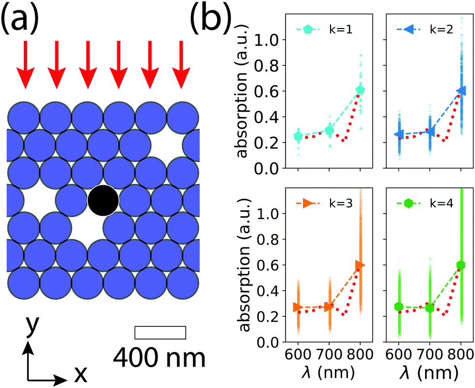 | ||
| Fig. 1 (a) Schematic geometry of a 2D omission glass. A GaAs cylinder absorber (black) is surrounded by a lattice of n = 41 SiO2 cylinders (blue). For this specific example, three SiO2 cylinders have been omitted from the structure, or k = 3. Illumination is incident from above (red arrows), with the polarization vector parallel to the cylindrical axis. For FDTD simulations, the geometry has periodic boundary conditions along the x-direction. (b) Integrated absorption spectra for k = 1–4 computed from the complete set of ensemble configurations. The dots represent the integrated absorption for each configuration to show the intrinsic physical variance in the ensemble. The k = 0 absorption spectrum (dashed red line) is plotted for comparison in each panel. | ||
Here, a single omission glass photoelectrode example is used to illustrate the ML emulator ensemble approach. The geometry of the omission glass photoelectrode is a 250 nm GaAs cylinder centered in a close-packed lattice of 250 nm SiO2 cylinders (n = 41, organized into 7 close-packed layers, Fig. 1a). FDTD simulations for calculating the steady-state electric field and absorption in the simulation volume were performed using the software package MEEP.17 Details of the implementation of the FDTD simulations and optical characterization of the close-packed, k = 0 photoelectrode are included in the ESI.† Each omission configuration for the k = 1, 2, 3, and 4 ensembles was simulated at incident wavelengths λ = 600 nm, 700 nm, and 800 nm (Fig. 1b). The brute-force, ensemble-averaged absorption spectra for k = 1 to k = 4 showed that increasing k from 0 to 4 has a small effect on absorption in the GaAs cylinder. Absorption increased at λ = 600 nm, from 0.231 to 0.276 (a 20% increase) and decreased at λ = 700 nm, from 0.311 to 0.264 (a 15% decrease). The per-configuration variability and absorption extrema for integrated absorption increased at all wavelengths for increasing k. The spatial organization of the k voids therefore can have a significant effect on the absorption for a given configuration within a single ensemble.
A multilayer perceptron (MLP)-based emulator was used to predict the two-dimensional absorption profile in the GaAs absorber for a given configuration of SiO2 scatterers. An MLP is an example of a supervised machine learning algorithm, meaning that it is trained on a subset of input–output observations to allow for predictions on all possible input signals. Assigning an addressable index to each of the n lattice positions provides a unique 41-bit, binary input representation for each configuration in the ensemble: ‘1’ for present scatterer at that site and ‘0’ for omission (Fig. S1, ESI†). For k = 3, each configuration is represented by a unique list of 38 ones and three zeros. An MLP emulator trained on a set of FDTD simulations acts as a function that can predict the absorption profile for the 41-bit representation of any omission glass configuration. The emulator studied here were implemented using the MLPregressor function in the scikit-learn Python library.18 Details of the representation of the simulation data and the MLP implementation parameters are described in the ESI.†
Beginning with the complete k = 1–4 ensembles allowed for the evaluation of the statistical accuracy of the MLP emulator compared to the true physical behavior of the ensemble. It also allowed for the evaluation of predictive accuracy in relation to the size of the training set and choice of included FDTD simulations. To supplement the k = 0–4 ensemble data, a library of randomly chosen FDTD simulations from each of the k = 5, k = 6, k = 8, and k = 10 ensembles was generated, including 20![[thin space (1/6-em)]](https://www.rsc.org/images/entities/char_2009.gif) 000 examples from each ensemble.
000 examples from each ensemble.
The per-pixel variance of a prediction to the true value, σpp, is a metric for quantifying the prediction accuracy of a trained emulator. The mathematical definition of σpp is included in the ESI.†Fig. 2 shows examples of Apred and AFDTD for randomly chosen k = 3 configurations by an MLP emulator trained on the complete set of k = 0–2 FDTD absorption profiles (862 total simulations) for λ = 600 nm. Additional examples of these predictions are shown in Fig. S2–S4 (ESI†). The spatial distribution and magnitude of Apred and AFDTD agreed qualitatively in general, but σpp quantified the accuracy of the prediction. A discussion regarding the statistical accuracy of MLP emulator predictions on single ensembles are included in the ESI.†
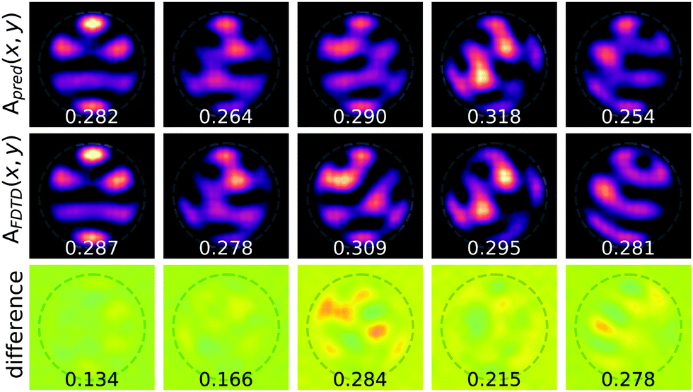 | ||
| Fig. 2 Randomly chosen examples of the MLP-predicted profile Apred, the corresponding true profile AFDTD, and the difference between the two profiles (difference). The integrated absorption (λ = 600 nm) for each profile is included at the bottom of each panel. The σpp metric for each pair is included at the bottom of the difference panel. | ||
To measure large scale prediction accuracy, the library of simulations (k ≤ 10) was used to train MLP emulators to measure prediction accuracy across each ensemble. The test set for each ensemble calculation of σpp used all simulations from the library excluding the ones used in the training set. Fig. 3a shows the effect that the distribution of simulations (λ = 600 nm) in a training set (Nset) of fixed size has on the accuracy. Each emulator was trained with a training set comprised of the complete k = 0–2 ensembles and Nset = 3000 simulations from the rest of the library, randomly selected in equal number from the contributing ensemble. For example, ‘k ≤ 4’ included 1500 simulations each from the k = 3 and k = 4 ensembles, and ‘k ≤ 10’ included 500 simulations each from the k = 3, k = 4, k = 5, k = 6, k = 8, and k = 10 ensembles. σpp values were low and relatively constant for predictions on the k = 2–5 ensembles regardless of the training set composition. As the number of ensembles represented in the training set increased, the accuracy of predictions for ensembles with larger k-values improved. For k = 10, σpp decreased from 0.192 for the ‘k ≤ 4’ emulator to 0.153 for the ‘k ≤ 10’ emulator. σpp showed similar decreases for simulations from ensembles (k = 7, k = 9) that were not included in the training set.
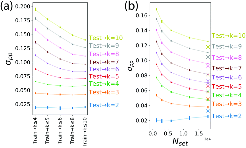 | ||
| Fig. 3 (a) σpp measurements for MLP emulators trained with a fixed number of samples (Nset = 3000) of varying distribution (described in text) across the ensembles in a library of λ = 600 nm FDTD simulations. No simulations from the k = 7 or k = 9 ensembles were included in the training set but were included as a test set. Each line represents the σpp measurement averaged over eight unique models. The solid bars represent the standard deviation of measurements. (b) σpp measurements for MLP emulators (solid lines) trained on the ‘k ≤ 10’ training set as a function of Nset. σpp was also calculated for varied contributions from each ensemble. The ‘X’ data represents σpp measurements for an emulator trained a training set of simulations skewed towards high k-values, consisting of the entire k = 0–2 ensembles, 500 simulations from k = 3, 500 from k = 4, 2500 from k = 5, 2500 from k = 6, 6000 from k = 8, and 6000 from k = 10. | ||
Increasing Nset showed a nearly uniform decrease σpp for most of the ensembles (Fig. 3b). σpp increased slightly for predictions in the k = 2 ensemble, for which all of the simulations are included in the training set. The increase in σpp can be attributed to the relative decrease in the total fraction of k = 2 simulations in the total training set. Using the same procedure, the distributions of random samples from each of the ensembles (k = 3–10) were modified to include more simulations from ensembles with larger k-values. Increasing the relative number of contributions to the training set from ensembles with large values of k resulted in a further reduction of σpp compared to the uniformly distributed examples. σpp slightly increased for predictions on the k = 2–6 ensembles due to the relative decrease in the representation of those ensembles in the training set.
The integrated absorption (λ = 600 nm) for Apred and AFDTD for each ensemble in the test set is shown in Fig. 4. Each unique simulation in the test set is represented by a point in the scatter plot. The absorption values predicted are in statistical agreement for configurations with low true values of absorption, as indicated by the symmetric and narrow clustering around the diagonal line (slope = 1). The clustering tends to be lower than the diagonal line for high true values of absorption, indicating that an MLP emulator tends to underestimate the absorption for those configurations. The as-trained emulator predicts that the ensemble-averaged absorption in the omission glass will increase with increasing k, which is consistent with the FDTD-derived absorption. At k = 10, the emulator predicts an absorption of 0.292, a 27% increase over the k = 0 electrode. While there is a significant difference between the predicted and true absorption values (0.310), the emulator captures the relationship between k and total absorption (see Fig. S8 and S9, ESI,† for λ = 700 nm and 800 nm).
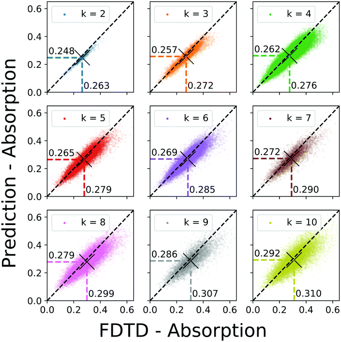 | ||
| Fig. 4 Scatter plots showing the distribution of integrated absorption values (λ = 600 nm) for each of the test data configurations, using an emulator trained on a training set consisting of the k = 0–2 ensembles, 500 simulations from k = 3, 500 from k = 4, 2500 from k = 5, 2500 from k = 6, 6000 from k = 8, and 6000 from k = 10. For each configuration in the ensemble, the x-coordinate of the point represents the FDTD-derived absorption for the configuration while the y-coordinate represents the MLP-predicted absorption. The black ‘X’ in each plot indicates the ensemble average of the predicted (y-coordinate) and the FDTD-determined true (x-coordinate) absorption. | ||
Here, this work has demonstrated that a neural network algorithm can be used to emulate the complex optical absorption properties of a disordered electrode design. An ML algorithm can infer the hidden correlations between different electrode configurations to predict the spatial distribution of absorption in a small-volume light absorber. Entire sets of ensembles can be approximated by this method with quantifiable accuracy while reducing the simulation cost (number of total simulations for ensemble calculations) by more than five orders of magnitude over the brute-force approach of simulating entire ensembles. Specifically, an MLP emulator can predict the absorption profiles and the assess the accuracy of prediction for the k = 0–10 ensembles of an omission glass (1.5 × 10⁹ unique configurations) with fewer than 104 simulations.
These results demonstrate the potential for using ML in the design of photoelectrodes for PEC applications. This can improve the computational efficiency for predicting the optical performance or incident photon-to-carrier conversion efficiency (IPCE) performance of device designs based on disordered materials. Emulation may have significant impact for IPCE prediction, which in general depends on the spatial distribution of absorption. This is particularly important in semiconductors with low minority carrier diffusion lengths where light trapping strategies are commonly used.19,20 As a direct application of this work, the MLP emulator can speed up calculations to identify the best performing combination of n (or density of GaAs cylinders), k (the omission fraction), and diameters of GaAs and SiO2 cylinders for a PEC solar-to-fuels electrode. Emulation can be applied more generally to continuously disordered materials, though it is necessary to identify a representation that uniquely describes the system structure and corresponding absorption profile.
A drawback for the MLP approach, and most neural network ML algorithms in general, is that the trained emulator does not provide physical insight to high or low performance structures or produce an analytical model that can be generally applied. An MLP algorithm simply acts as a highly parameterized fitting function that can infer correlations between electrode structures and absorption profiles. The ability to make structure–function predictions as described here can spur further statistical analysis to identify the principal factors affecting variance in the absorption profile or otherwise be used to improve the accuracy of the emulators through rational choice of simulations for the training data. Understanding the factors that affect the absorption profile may encourage the development of new fabrication methods to enhance power conversion efficiency in PEC or photocatalytic devices.
This material is based upon work supported by the U.S. Department of Energy, Office of Science, Office of Basic Energy Sciences under Award Number DE-SC-0020301.
Conflicts of interest
There are no conflicts to declare.Notes and references
- X. Chen, J. Ye, S. Ouyang, T. Kako, Z. Li and Z. Zou, ACS Nano, 2011, 5, 4310–4318 CrossRef CAS PubMed.
- R. H. Coridan, K. A. Arpin, B. S. Brunschwig, P. V. Braun and N. S. Lewis, Nano Lett., 2014, 14, 2310–2317 CrossRef CAS PubMed.
- M. Zhou, J. Bao, Y. Xu, J. Zhang, J. Xie, M. Guan, C. Wang, L. Wen, Y. Lei and Y. Xie, ACS Nano, 2014, 8, 7088–7098 CrossRef CAS PubMed.
- M. Curti, J. Schneider, D. W. Bahnemann and C. B. Mendive, J. Phys. Chem. Lett., 2015, 6, 3903–3910 CrossRef CAS PubMed.
- J. D. Joannopoulos, S. G. Johnson, J. N. Winn and R. D. Meade, Photonic Crystals: Molding the Flow of Light, Princeton University Press, 2nd edn, 2011 Search PubMed.
- E. Armstrong and C. O’Dwyer, J. Mater. Chem. C, 2015, 3, 6109–6143 RSC.
- P. Jiang, J. F. Bertone, K. S. Hwang and V. L. Colvin, Chem. Mater., 1999, 11, 2132–2140 CrossRef CAS.
- C. Xiang, A. Z. Weber, S. Ardo, A. Berger, Y. Chen, R. Coridan, K. T. Fountaine, S. Haussener, S. Hu, R. Liu, N. S. Lewis, M. A. Modestino, M. M. Shaner, M. R. Singh, J. C. Stevens, K. Sun and K. Walczak, Angew. Chem., Int. Ed., 2016, 55, 12974–12988 CrossRef CAS PubMed.
- S. Suter, M. Cantoni, Y. K. Gaudy, S. Pokrant and S. Haussener, Sustainable Energy Fuels, 2018, 2, 2661–2673 RSC.
- D. S. Wiersma, Nat. Photonics, 2013, 7, 188–196 CrossRef CAS.
- D. S. Wiersma, Nat. Phys., 2008, 4, 359–367 Search PubMed.
- N. J. Hogan, A. S. Urban, C. Ayala-Orozco, A. Pimpinelli, P. Nordlander and N. J. Halas, Nano Lett., 2014, 14, 4640–4645 CrossRef CAS PubMed.
- Y. Zhai, Y. Ma, S. N. David, D. Zhao, R. Lou, G. Tan, R. Yang and X. Yin, Science, 2017, 355, 1062–1066 CrossRef CAS PubMed.
- J. Mandal, Y. Fu, A. C. Overvig, M. Jia, K. Sun, N. N. Shi, H. Zhou, X. Xiao, N. Yu and Y. Yang, Science, 2018, 362, 315–319 CrossRef CAS PubMed.
- M. A. Norman, W. L. Perez, C. C. Kline and R. H. Coridan, Adv. Funct. Mater., 2018, 28, 1800481 CrossRef.
- R. H. Coridan, M. A. Norman and H. Mehrabi, Can. J. Chem., 2018, 96, 969–973 CrossRef CAS.
- A. F. Oskooi, D. Roundy, M. Ibanescu, P. Bermel, J. D. Joannopoulos and S. G. Johnson, Comput. Phys. Commun., 2010, 181, 687–702 CrossRef CAS.
- F. Pedregosa, G. Varoquaux, A. Gramfort, V. Michel, B. Thirion, O. Grisel, M. Blondel, P. Prettenhofer, R. Weiss, V. Dubourg, J. Vanderplas, A. Passos, D. Cournapeau, M. Brucher, M. Perrot and É. Duchesnay, J. Mach. Learn. Res., 2011, 12, 2825–2830 Search PubMed.
- B. M. Kayes, H. A. Atwater and N. S. Lewis, J. Appl. Phys., 2005, 97, 114302 CrossRef.
- H. Dotan, O. Kfir, E. Sharlin, O. Blank, M. Gross, I. Dumchin, G. Ankonina and A. Rothschild, Nat. Mater., 2013, 12, 158–164 CrossRef CAS PubMed.
Footnote |
| † Electronic supplementary information (ESI) available. See DOI: 10.1039/d0cc04229c |
| This journal is © The Royal Society of Chemistry 2020 |