
 Open Access Article
 This Open Access Article is licensed under a Creative Commons Attribution-Non Commercial 3.0 Unported Licence
COvalent monolayer patterns in Microfluidics by PLasma etching Open Technology – COMPLOT†
Stan B. J.
Willems
 abc,
Jaccoline
Zegers
a,
Anton
Bunschoten
ac,
R. Martijn
Wagterveld
b,
Fijs W. B.
van Leeuwen
ac,
Aldrik H.
Velders
ac and
Vittorio
Saggiomo
*a
abc,
Jaccoline
Zegers
a,
Anton
Bunschoten
ac,
R. Martijn
Wagterveld
b,
Fijs W. B.
van Leeuwen
ac,
Aldrik H.
Velders
ac and
Vittorio
Saggiomo
*a
aLaboratory of BioNanoTechnology, Wageningen University and Research, Bornse Weilanden 9, 6708 WG Wageningen, the Netherlands. E-mail: vittorio.saggiomo@wur.nl
bWetsus, European Centre of Excellence for Sustainable Water Technology, Oostergoweg 9, 8911 MA Leeuwarden, the Netherlands
cInterventional Molecular Imaging, Department of Radiology, Leiden University and Medical Centre, 2300 RC Leiden, the Netherlands
First published on 13th January 2020
Abstract
Plasma microcontact patterning (PμCP) and replica molding were combined to make PDMS/glass microfluidic devices with β-cyclodextrin (β-CD) patterns attached covalently on the glass surface inside microchannels. The supramolecular reactivity, reusability and association constant of β-CD with Cy5–Ad2 was tested by analyzing signal-to-noise ratios of patterns vs. spacing with fluorescence microscopy.
Introduction
(Bio)sensors using chemically modified surfaces have proven instrumental for the sensitive detection of (bio)analytes.1–6 Therefore, the incorporation of modified surfaces within a microfluidic device is becoming an attractive field for creating lab-on-a-chip platforms, e.g. the detection of enzymes on chitosan functionalized surfaces.7 Within microfluidic devices, the fabrication of polydimethylsiloxane (PDMS)/glass hybrid systems are highly popular because of their versatility and low-cost.8,9 These microfluidic devices allow for facile fluid handling, can analyze small volumes and support direct analyte analysis using microscopy.10 Subsequently, analyte quantification defines the final utility of the microfluidic sensor. In light of this, analyte binding to patterns of molecules within the microfluidic device can be compared with non-functionalized (control) spacing in one field of view in order to quickly establish signal to background ratio's.11The fabrication of PDMS/glass microfluidic devices, also known as ‘replica molding’,12 works by activation of the PDMS replica containing micro-sized grooves with a glass surface in the plasma oven, and subsequently applying conformal contact between PDMS and glass surface. The grooves in the PDMS replica form a microchannel with desired size features on the glass surface and the microfluidic device is sealed. When the two surfaces are in contact the silanols react to form silyl ethers and covalently ‘seal’ PDMS to glass, forming a mixed PDMS/glass microfluidic device.13 One major drawback of this methodology is that creating patterns of molecules on the glass surface before plasma treatment is not feasible, as the plasma exposure for sealing the microfluidic device will remove the molecular patterns.
We have recently shown that plasma etching, in combination with plasma microcontact patterning (PμCP), is a reproducible method for creating patterns of covalently bound molecules on glass surfaces.14 In brief, a PDMS stamp, of the kind normally used for microcontact printing (μCP), is placed in contact with a covalently modified glass surface and the construct is subjected to plasma etching. Exposed molecules which are not protected by the PDMS stamp are decomposed by plasma, resulting in molecular patterns. It should be noted that the PDMS ‘stamp’ is now actually functioning as a ‘mask’: instead of adding molecular patterns to the surface through ‘stamping’ as with μCP, patterns are now generated by removing molecular functionality through plasma etching from those areas where the PDMS stamp is not in contact with the surface. Another important advantage with PμCP is that the plasma exposed regions between the stamp patterns and outside the stamp area now contain reactive silanols which can be used for covalent bonding with PDMS surfaces. Based on this utility, we speculated that in order to create a microfluidic device with embedded patterns of covalently functionalized monolayer patterns, PμCP could be combined with PDMS replica molding. Previously, this concept has only been carried out to create surfaces that contain patterns of physisorbed proteins within microfluidic channels.15,16 More labor intensive methods, without patterns, involve the manufacturing of glass–glass microfluidic systems using vacuum UV light or fluorosilanes in combination with piranha etching.17,18
We are advocating Open Technologies such as ESCARGOT,19 for cheap microfluidics and HARICOT,20 for responsive materials: here we present the COMPLOT concept: COvalent monolayer patterns in Microfluidics by PLasma etching Open Technology. Therefore, introducing covalent surface modification, as presented here, provides the user with a reliable and cost-friendly patterning methodology that can simply be incorporated in microfluidic channels for simple qualitative as well as more advanced and quantitative applications.
As proof of concept for combined PμCP/replica molding with a covalent modified surface, we investigated the fabrication of β-cyclodextrin (β-CD) patterns within a microfluidic device (Fig. 1). Cyclodextrins are well known for their applications in food technology, pharmaceutics and drug delivery, but have also emerged as versatile platforms for material science through their interactions with metal ions and inorganic nanoparticles.21 Through supramolecular host–guest chemistry, the inside of β-CD's hydrophobic cavity (host) can be used for immobilization of guest functionalized molecules, such as Cyanine 5-diadamantane (Cy5–Ad2, structure in Fig. S1, ESI†),22 or for capturing adamantane modified microparticles on flow through host–guest chemistry.23 Here, we validated the functionalization of β-CD patterns on the glass surface within the fabricated microfluidic device through addition of Cy5–Ad2, which allowed us to use fluorescence microscopy to study the immobilization and release of Cy5–Ad2 under flow. In addition, the binding kinetics of Cy5–Ad2 were also determined in a multichannel COMPLOT device via analysis of different Cy5–Ad2 concentrations on one microfluidic slide.
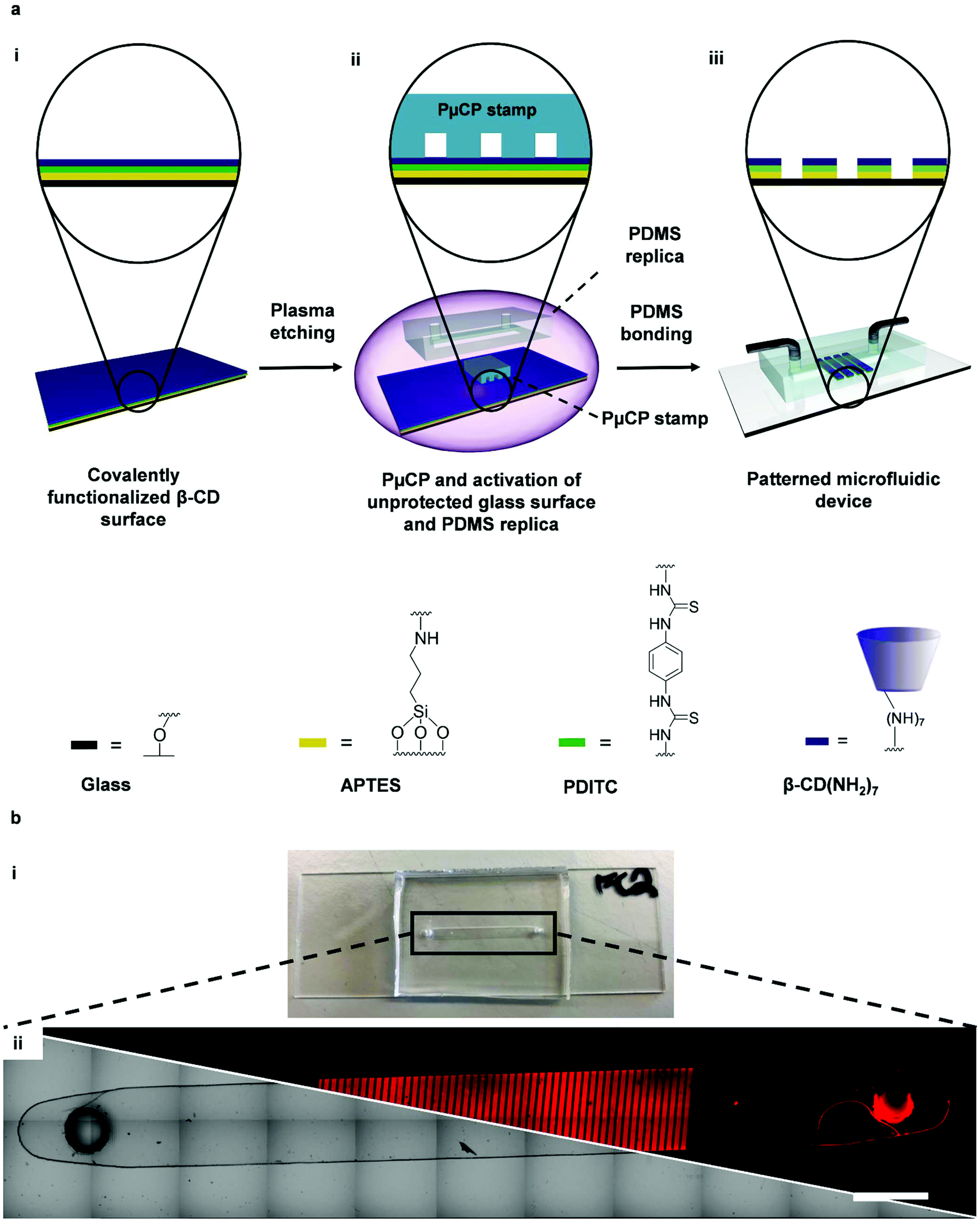 | ||
| Fig. 1 (a) Scheme showing the fabrication of the patterned microfluidic device: a fully functionalized β-CD surface is obtained after silanization with 3-aminopropyltriethoxysilane (APTES) and 1,4-phenelynediisothiocyanate (PDITC) cross linking of heptakis amino β-CD (i), then a PDMS stamp with line features is placed on top of modified surface for PμCP and plasma etched together with the PDMS replica (ii), and finally the PDMS replica is chemically bonded to the patterned β-CD surface via plasma bonding to create a β-CD patterned microfluidic device (iii). (b) Photograph of a single channel patterned microfluidic device (i) and microscope images of channel using 5× objective and 11 × 2 tile scan after addition of Cy5–Ad2 using the Brightfield (lower left) and Cy5–fluorescence (upper right) settings (ii) (scale bar is 2 mm). | ||
Results and discussion
Fig. 1a illustrates the steps required for microfluidic device fabrication. A fully functionalized β-CD surface was first obtained following a literature protocol from Onclin et al.24 (Fig. 1a(i)): the glass functionalization with heptakis amino β-CD was carried out using 3-aminopropyltriethoxysilane (APTES) for obtaining an amine functionalized surface, 1,4-phenylenediisothiocyanate (PDITC) for creating an amine reactive surface, and finally incubation of heptakis amino β-CD. Surface patterning of β-CD was realized via PμCP with a PDMS stamp molded from a silicon wafer that was patterned through UV-lithography (150 μm broad line features and 50 μm broad spacing with 50 μm height, cut to about 0.75 cm2; four plasma cycles of 1 min).14,25 PμCP also generates a reactive surface for subsequent microchannel fabrication (Fig. 1a(ii)). The size of the PDMS stamp, along with the length and width of the spacing between features on the PDMS stamp, were chosen to achieve sufficient penetration of plasma gas molecules through the PDMS stamp spacing for etching the modified glass surface. Furthermore, the resolution of features can also be limited by UV-lithography fabrication of silicon substrates, which is >10 μm without a clean-room. Previously, we reached sub-10 μm resolution by rotating the PDMS stamp during PμCP of a functionalized surface, which removes more of the surface functionalization.14In parallel, PDMS was poured into a 3D printed mold containing a ridge of size 20 × 2 × 0.5 mm (length × width × height), forming the PDMS replica after curing in the oven. This will form a microchannel over the glass surface with a volume of 20 μL. The PDMS replica was activated in the plasma oven along with the stamp protected patterns for the final plasma cycle of 1 min, which ensures high quality and irreversible plasma bonding between the PDMS replica and glass surface (Fig. 1a(ii)).26 Following the plasma treatment, the stamp was removed from the glass surface and the activated PDMS replica was then placed on the patterned β-CD glass surface to chemically attach the PDMS to the glass surface, creating a microfluidic channel over the patterned area (Fig. 1a(iii)). In order to promote homogenous sealing of the microfluidic device, we ensured conformal contact between the PDMS replica and glass surface, then attached clamps to keep the microchannel firmly pressed against the glass surface which was followed by further bonding in the oven (Fig. S2, ESI†). The resulting microfluidic device is depicted in Fig. 1b.
Confirmation of β-CD pattern formation was realized by flowing a 0.23 μM solution of Cy5–Ad2 through the microfluidic device for 15 min at 50 μL min−1. Excess Cy5–Ad2 was washed away with PBS and DI water, resulting in clear 150 μm broad line patterns when analyzed with a fluorescence microscope (Fig. 1b(ii)). Importantly, no binding of Cy5–Ad2 was noticed outside the β-CD patterned area, which serves as an additional control for the analyte detection. A more detailed sequence of events is depicted in Fig. S3 (ESI†) showing the microscope images of surface before Cy5–Ad2 addition, during addition and after washing away excess Cy5–Ad2 with PBS and DI water. After washing away excess Cy5–Ad2, the fluorescence intensity of remaining Cy5–Ad2 on β-CD is generally ca. 4 times higher than the background signal between patterns, which is a result of the high affinity divalent host–guest interactions between Cy5–Ad2 and β-CD (Fig. S3b(ii), ESI†). We also illustrated the Cy5–Ad2 addition and washing steps by carrying out a time lapse experiment coupled with a live profile plot that follows the fluorescence intensity during these events (Video S1†). Cy5–Ad2 addition is carried out within 1 min at 50 μL min−1 flow rate and shows a bright signal over the whole surface. Consecutively washing the surface with PBS at 200 μL min−1 decreases the fluorescence intensity to show clear patterns of Cy5–Ad2 adhered to β-CD already within 2 min, which correlates with the situations depicted in Fig. S3 (ESI†).
An important characteristic of (bio)sensors incorporated within simple microfluidic devices is re-usability of the sensor in order to run different analytical experiments over the same sensor. In our case, supramolecular host–guest chemistry of β-CD with adamantane guest molecules allows for non-covalent, reversible interactions.27 Hence, stripping the surface of immobilized Cy5–Ad2 analytes was also studied using a known procedure based on removal of diadamantane functionalized guest molecules with 10 mM β-CD,28 which was carried out using a flow rate of 800 μL min−1. In Fig. 2a, the 1st removal of Cy5–Ad2 and subsequent repeat addition and removal are shown. From the profile plots it should be noted that the intensity values were normalized for the minimal values within the graph (normalizing the spacing intensity to 1). Fig. 2b illustrates that the printed surface was tested for a total of 4 additions of Cy5–Ad2 and that the loading-rate diminishes by approximately 10% in the consecutive recycling steps, but the pattern intensity remains preserved at ca. 3.5 as shown for the 3rd and 4th uses. The washing step with β-CD does not completely remove immobilized Cy5–Ad2 (Fig. 2a(ii) and (iv)). However, the average pattern intensity after removal remains approximately between 1–1.5 for all removal steps which indicates reversibility is reproducible (Fig. 2b). The sensor technology presented holds potential for monitoring extraction and release of analytes through supramolecular interactions for guest molecules which have similar binding affinities as Cy5–Ad2 (approximately between 107–1010 M−1 in aqueous solutions).29,30
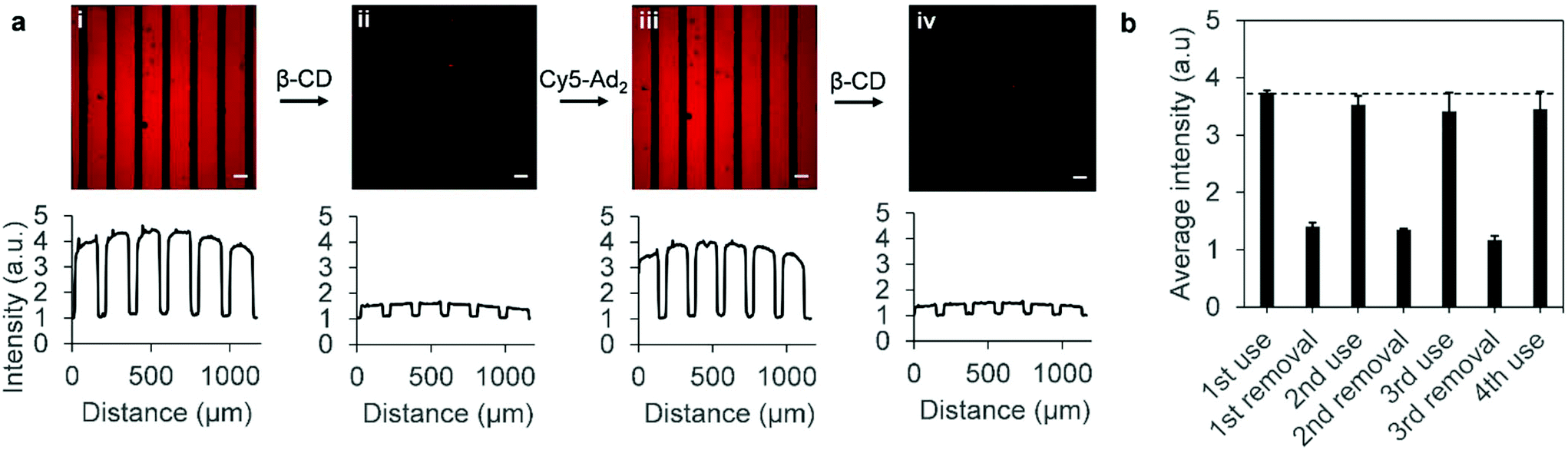 | ||
| Fig. 2 (a) Re-usability of microfluidic devices showing β-CD patterned surface after addition and washing away excess Cy5–Ad2 (i), after removal of immobilized Cy5–Ad2 by washing with β-CD solution (ii), after 2nd addition and washing away excess Cy5–Ad2 (iii), and after 2nd removal of immobilized Cy5–Ad2 by washing with β-CD solution (iv). Images were taken at the same location to allow for fair comparison and were captured with 10× objective. Scale bars are 100 μm. The profile plots below the images show the normalized intensity of patterns and spacing vs. the distance. (b) Graph showing the average pattern intensity for 4 uses/additions of Cy5–Ad2 and 3 removals with β-CD. Error bars represent standard deviation in average pattern intensity determined from the profile plot of each image. | ||
Within lab-on-a-chip technology, the fabrication of (bio)arrays for carrying out multiple analyses using one chip is quite popular. This is also particularly useful for analyzing binding kinetics of analytes through varying analyte concentration. In this case, using one surface increases the accuracy of the quantitative analysis with techniques such as fluorescence microscopy. The inclusion of analyte binding patterns on the sensor also further improves the quantitative analysis by providing the user with a signal-to-noise ratio. To demonstrate the utility of our microfluidic device in such a test, we exchanged the single channel PDMS device for a multiple channel one containing 5 channels with the same groove dimensions as used before. The PμCP step on β-CD functionalized surfaces was slightly modified to incorporate β-CD patterns within all 5 channels: before plasma etching, PμCP stamps were cut in 5 pieces, with each piece having approximately the same width of one microchannel, and then placed on the β-CD glass surface (Fig. 3a). At this stage it is important that sufficient space (approximately 2 mm) is left between the PμCP stamps and that the stamps are placed within the area where the microchannels will be formed when bonding the PDMS replica. Otherwise, resulting patterns of β-CD will overlap neighboring channels, which hinders proper sealing of the PDMS replica between channels and causes leaching of solution from one channel to another.
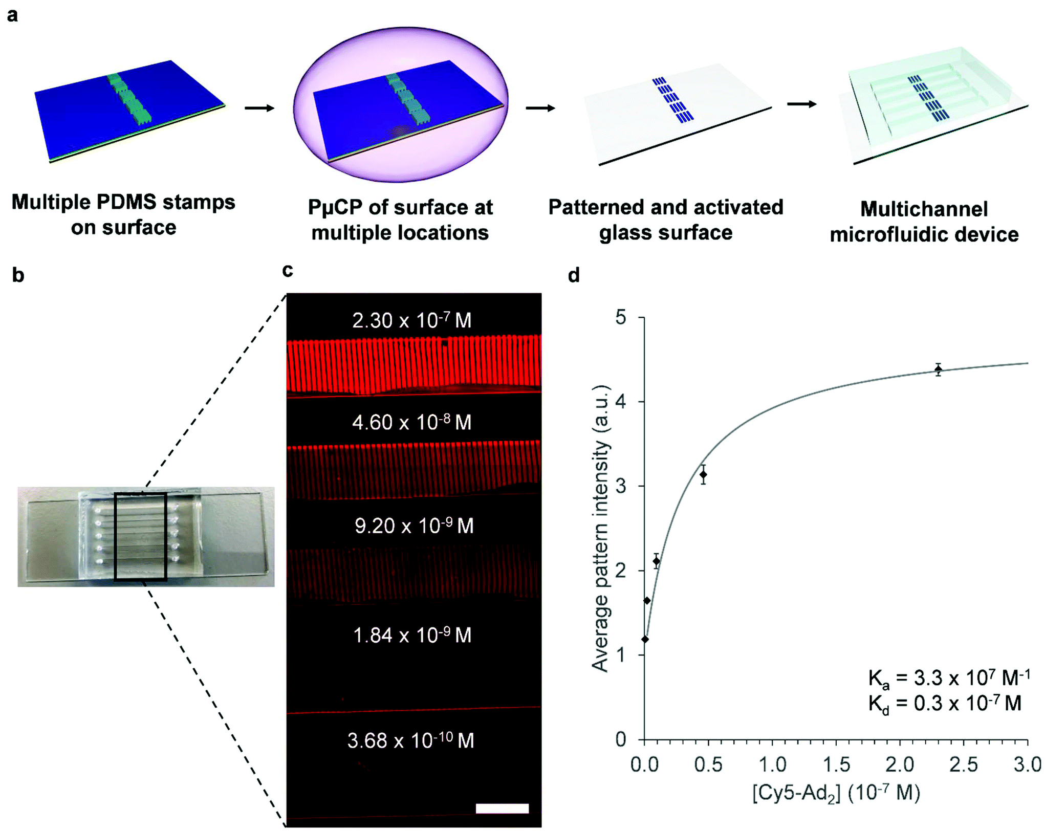 | ||
| Fig. 3 (a) Scheme explaining fabrication of multichannel microfluidic device with β-CD patterns (b) Photograph of patterned microfluidic device with 5 channels. (c) Microscope image of area depicted in (b) after addition of different concentrations of Cy5–Ad2. The concentration used is written above the designated microchannel. The image was captured using a 5× objective and 8 × 4 tilescan. Scale bar is 2 mm. (d) Graph showing the average pattern intensity obtained with the different concentrations of Cy5–Ad2 used. The binding (Ka) and dissociation (Kd) constants are also shown which are based on fitting results to the Langmuir equation. Error bars represent standard deviation in average pattern intensity determined from profile plots of microscope images from each channel. | ||
Next, 5× serial dilution of a Cy5–Ad2 solution was made and flowed over the β-CD patterned microfluidic device with multiple channels (Fig. 3b), starting from the highest concentration (top channel) to the lowest concentration (bottom channel) (Fig. 3c). A sharp increase in fluorescence intensity was observed close to the channel walls i.e. a so-called ‘edge’ effect. This could be attributed to reflection of the PDMS channel wall when using fluorescence microscopy and was therefore not included in the quantitative analysis. The average pattern intensity in Fig. 3d was determined by capturing images of each microchannel using the 10× objective and normalizing profile plots for the minimal values, i.e. spacing between β-CD patterns. Moreover, a control experiment with 0.23 μM of Cy5–Ad2 was carried out to show that using multiple strips of PDMS stamps during the PμCP step does not significantly alter the density of β-CD units over the different patterned areas on one surface (Fig. S4, ESI†). As expected, the fluorescence increases when higher concentrations of Cy5–Ad2 are used, and the trend in the graph resembles a typical binding affinity profile when fitted to the Langmuir adsorption model (Fig. 3d).‡ Although Cy5–Ad2 binds in a divalent fashion with β-CD units on the surface, it should be noted that by using the Langmuir equation the overall binding affinity is determined. When analyzing more complex samples (e.g. proteins that contain several binding sites), determining the intrinsic binding affinity and effective molarity of a single interaction pair can give more details about relevant binding kinetics.30–32 Fitting the data allowed for determining a Cy5–Ad2 dissociation constant (Kd, the analyte concentration at half of the maximum fluorescence) of 0.3 × 10⁻⁷ M for β-CD patterns which yields an overall binding constant (Ka) of 3.3 × 10⁷ M−1. The acquired binding constant is in line with expectations for divalent host–guest interactions for the β-CD cavity and adamantane.29,30 These results show that these patterned microfluidic devices can also be used for carrying out analysis of different concentrations of analytes and suggest that they could also be used for comparing binding affinity of different analytes on one surface.
Conclusions
In this work, we introduce COMPLOT technology: covalent monolayer patterns in Microfluidics by Plasma etching Open Technology. Microfluidic devices were fabricated containing covalently functionalized molecular patterns at the inside of the channel wall by combining plasma microcontact patterning (PμCP) and replica molding. Incorporation of the patterned surfaces in the microfluidic device allows for simple fluid handling and approaching sensor applications within aqueous flow streams. As a proof of concept for sensing applications, we studied the reversible host–guest interactions between patterns of β-CD, included within the microfluidic device, and Cy5–Ad2. The immobilization and removal of Cy5–Ad2 was easily analyzed using a fluorescence microscope and it was possible to re-use the β-CD patterned microfluidic device several times, which is beneficial for extraction applications and avoids laborious repetition of the surface functionalization. It is also possible to study binding of several analytes on one surface through creating a microfluidic device with multiple channels, all containing β-CD patterns. For this, we looked into determining the binding constant of Cy5–Ad2 for β-CD layers, which correlated with expectations for diadamantane functionalized molecules. β-CD modified surfaces could also be used as selective “turn-off” colorimetric sensors for quantitative detection of heavy metal ions in aqueous streams.33,34 Furthermore, the versatility of the adamantane-β-CD couple is similar to the (strept)avidin–biotin couple, and therefore allows for incorporating (bio)molecules functionalized with adamantane on the surface. Alternatively, COMPLOT can be used for incorporating other molecules for the surface functionalization besides β-CD. In principle, any molecule containing a primary amine can be patterned in the microfluidic device using the same methodology presented here, e.g. biotin-NH2, amino sugars for lectin detection or antibodies for antigen detection, provided the (bio)sensor's functionality is preserved after attachment to the surface. The microfluidic device can be used for various applications with aqueous or light organic solvents such as ethanol and methanol, however, use of highly hydrophobic solvents which swell PDMS, such as toluene or chloroform should be avoided. Through this enabling technology for fabrication of patterned PDMS/glass hybrid microfluidic devices, a way is opened for researchers less experienced in surface functionalization and working on different fields ranging from (bio) sensing applications, such as immobilization of micron-sized entities,23 to analytical chemistry and medical applications like lab- or organs-on-a-chip.35,36Conflicts of interest
There are no conflicts to declare.Acknowledgements
This work was performed in the cooperation framework of Wetsus, European Centre of Excellence for Sustainable Water Technology (http://www.wetsus.eu). Wetsus is co-funded by the Dutch Ministry of Economic Affairs and Ministry of Infrastructure and Environment, the Province of Fryslân, and the Northern Netherlands Provinces. The authors like to thank the members of the research theme Source Separated Sanitation for the shared knowledge and financial support. We acknowledge Mark Rood for preparing the Cy5–Ad2 dye.Notes and references
- A. Kumar, H. A. Biebuyck and G. M. Whitesides, Langmuir, 1994, 10, 1498–1511 CrossRef CAS.
- M. Mrksich and G. M. Whitesides, Annu. Rev. Biophys. Biomol. Struct., 1996, 25, 55–78 CrossRef CAS PubMed.
- S.-H. Hsu, M. D. Yilmaz, C. Blum, V. Subramaniam, D. N. Reinhoudt, A. H. Velders and J. Huskens, J. Am. Chem. Soc., 2009, 131, 12567–12569 CrossRef CAS PubMed.
- D. Dorokhin, S.-H. Hsu, N. Tomczak, D. N. Reinhoudt, J. Huskens, A. H. Velders and G. J. Vancso, ACS Nano, 2010, 4, 137–142 CrossRef CAS PubMed.
- A. Gonzalez-Campo, S. H. Hsu, L. Puig, J. Huskens, D. N. Reinhoudt and A. H. Velders, J. Am. Chem. Soc., 2010, 132, 11434–11436 CrossRef CAS PubMed.
- R. de laRica, R. M. Fratila, A. Szarpak, J. Huskens and A. H. Velders, Angew. Chem., Int. Ed., 2011, 50, 5704–5707 CrossRef CAS PubMed.
- Z. Wang, L. He, J. Lv and M. Kimura, Mater. Res. Express, 2019, 6, 045403 CrossRef.
- J. C. McDonald and G. M. Whitesides, Acc. Chem. Res., 2002, 35, 491–499 CrossRef CAS PubMed.
- K. Ren, J. Zhou and H. Wu, Acc. Chem. Res., 2013, 46, 2396–2406 CrossRef CAS PubMed.
- J. P. Lafleur, A. Jönsson, S. Senkbeil and J. P. Kutter, Biosens. Bioelectron., 2016, 76, 213–233 CrossRef CAS PubMed.
- R. S. Kane, S. Takayama, E. Ostuni, D. E. Ingber and G. M. Whitesides, in The Biomaterials: Silver Jubilee Compendium, ed. D. F. Williams, Elsevier Science, Oxford, 1999, pp. 161–174, DOI:10.1016/B978-008045154-1.50020-4.
- Y. Xia, J. J. McClelland, R. Gupta, D. Qin, X.-M. Zhao, L. L. Sohn, R. J. Celotta and G. M. Whitesides, Adv. Mater., 1997, 9, 147–149 CrossRef CAS.
- D. C. Duffy, J. C. McDonald, O. J. A. Schueller and G. M. Whitesides, Anal. Chem., 1998, 70, 4974–4984 CrossRef CAS PubMed.
- S. B. J. Willems, L. M. I. Schijven, A. Bunschoten, F. W. B. van Leeuwen, A. H. Velders and V. Saggiomo, Chem. Commun., 2019, 55, 7667–7670 RSC.
- S. W. Rhee, A. M. Taylor, C. H. Tu, D. H. Cribbs, C. W. Cotman and N. L. Jeon, Lab Chip, 2005, 5, 102–107 RSC.
- M. Rosso, V. van Steijn, L. C. P. M. de Smet, E. J. R. Sudhölter, C. R. Kleijn and M. T. Kreutzer, Appl. Phys. Lett., 2011, 98, 174102 CrossRef.
- K. Shirai, K. Mawatari and T. Kitamori, Small, 2014, 10, 1514–1522 CrossRef CAS PubMed.
- S.-I. Funano, N. Ota, A. Sato and Y. Tanaka, Chem. Commun., 2017, 53, 11193–11196 RSC.
- V. Saggiomo and A. H. Velders, Adv. Sci., 2015, 2, 1500125 CrossRef PubMed.
- A. H. Velders, J. A. Dijksman and V. Saggiomo, Appl. Mater. Today, 2017, 9, 271–275 CrossRef.
- D. Prochowicz, A. Kornowicz and J. Lewiński, Chem. Rev., 2017, 117, 13461–13501 CrossRef CAS PubMed.
- M. T. M. Rood, S. J. Spa, M. M. Welling, J. B. ten Hove, D. M. van Willigen, T. Buckle, A. H. Velders and F. W. B. van Leeuwen, Sci. Rep., 2017, 7, 39908 CrossRef CAS PubMed.
- S. B. J. Willems, A. Bunschoten, R. M. Wagterveld, F. W. B. van Leeuwen and A. H. Velders, ACS Appl. Mater. Interfaces, 2019, 11, 36221–36231 CrossRef CAS PubMed.
- S. Onclin, A. Mulder, J. Huskens, B. J. Ravoo and D. N. Reinhoudt, Langmuir, 2004, 20, 5460–5466 CrossRef CAS PubMed.
- R. Picone, B. Baum and R. McKendry, in Methods in Cell Biology, ed. M. Piel and M. Théry, Academic Press, 2014, vol. 119, pp. 73–90 Search PubMed.
- B. Millare, M. Thomas, A. Ferreira, H. Xu, M. Holesinger and V. I. Vullev, Langmuir, 2008, 24, 13218–13224 CrossRef CAS PubMed.
- G. Chen and M. Jiang, Chem. Soc. Rev., 2011, 40, 2254–2266 RSC.
- A. Mulder, S. Onclin, M. Peter, J. P. Hoogenboom, H. Beijleveld, J. ter Maat, M. F. Garcia-Parajo, B. J. Ravoo, J. Huskens, N. F. van Hulst and D. N. Reinhoudt, Small, 2005, 1, 242–253 CrossRef CAS PubMed.
- A. Mulder, T. Auletta, A. Sartori, S. Del Ciotto, A. Casnati, R. Ungaro, J. Huskens and D. N. Reinhoudt, J. Am. Chem. Soc., 2004, 126, 6627–6636 CrossRef CAS PubMed.
- J. Huskens, A. Mulder, T. Auletta, C. A. Nijhuis, M. J. W. Ludden and D. N. Reinhoudt, J. Am. Chem. Soc., 2004, 126, 6784–6797 CrossRef CAS PubMed.
- A. Perl, A. Gomez-Casado, D. Thompson, H. H. Dam, P. Jonkheijm, D. N. Reinhoudt and J. Huskens, Nat. Chem., 2011, 3, 317–322 CrossRef CAS PubMed.
- D. Di Iorio, M. L. Verheijden, E. van der Vries, P. Jonkheijm and J. Huskens, ACS Nano, 2019, 13, 3413–3423 CrossRef CAS PubMed.
- P. Suresh, I. A. Azath and K. Pitchumani, Sens. Actuators, B, 2010, 146, 273–277 CrossRef CAS.
- K. Kanagaraj, K. Bavanidevi, T. J. Chow and K. Pitchumani, RSC Adv., 2014, 4, 11714–11722 RSC.
- A. Polini, L. Prodanov, N. S. Bhise, V. Manoharan, M. R. Dokmeci and A. Khademhosseini, Expert Opin. Drug Discovery, 2014, 9, 335–352 CrossRef CAS PubMed.
- P. S. Dittrich and A. Manz, Nat. Rev. Drug Discovery, 2006, 5, 210–218 CrossRef CAS PubMed.
Footnotes |
| † Electronic supplementary information (ESI) available. See DOI: 10.1039/c9an02407g |
| ‡ In our case, the Langmuir adsorption model is represented by the equation: y = Kdx/(ymax + x) + 1, where y is the average fluorescent pattern intensity, ymax is the maximum amount of fluorescent pattern intensity subtracted by 1, and x is the concentration of Cy5–Ad2 in solution. The y values in the equation are corrected by adding 1 because the experimental pattern ratio starts at 1. |
| This journal is © The Royal Society of Chemistry 2020 |