 Open Access Article
Creative Commons Attribution 3.0 Unported Licence
Correction: Electrochemically deposited nanocrystalline InSb thin films and their electrical properties
K. E.
Hnida
*a,
S.
Bäßler
b,
J.
Mech
c,
K.
Szaciłowski
a,
R. P.
Socha
d,
M.
Gajewska
a,
K.
Nielsch
be,
M.
Przybylski
af and
G. D.
Sulka
g
aAGH University of Science and Technology, Academic Centre for Materials and Nanotechnology, al. A. Mickiewicza 30, 30-059 Krakow, Poland. E-mail: khnida@agh.edu.pl; katarzyna.hnida@gmail.com; Tel: +48 12 617 52 82
bUniversity of Hamburg, Multifunctional Nanostructures, Institute of Nanostructure and Solid State Physics, Jungiusstrasse 11, 20-355 Hamburg, Germany
cAGH University of Science and Technology, Faculty of Non-Ferrous Metals, Al. A. Mickiewicza 30, 30-059 Krakow, Poland
dJerzy Haber Institute of Catalysis and Surface Chemistry Polish Academy of Sciences, Niezapominajek 8, 30-239 Krakow, Poland
eLeibniz Institute for Solid State and Materials Research Dresden, PO Box 270116, 01171 Dresden, Germany
fAGH University of Science and Technology, Faculty of Physics and Applied Computer Science, al. A. Mickiewicza 30, 30-059 Krakow, Poland
gJagiellonian University in Krakow, Department of Physical Chemistry and Electrochemistry, Ingardena 3, 30-060 Krakow, Poland
First published on 17th May 2019
Abstract
Correction for ‘Electrochemically deposited nanocrystalline InSb thin films and their electrical properties’ by K. E. Hnida et al., J. Mater. Chem. C, 2016, 4, 1345–1350.
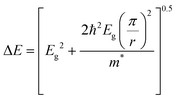
There was an error in eqn (3) which was reproduced from the literature and used for the interpretation of the results. The calculations (using the equations from an original work from 1987) were done according the correct version of eqn (3) presented below:
The obtained values show a decreased contribution of the quantum size effect to the Eg value. The quantum effect and Burstein–Moss effect contributions are now: 0.12 eV and 0.24 eV, respectively. Recalculated values of carrier concentration and mobility in InSb nanocrystalline films are gathered in Table 1.
| Recalculated | |
|---|---|
| Effective energy band gap | 0.29 eV |
| Quantum effect contribution | 0.12 eV |
| Burstein–Moss effect contribution | 0.24 eV |
| Carrier concentration n | 4.10 × 1017 cm−3 |
| Carrier mobility μ | 31.4 cm2 V−1 s−1 |
The change in the value of the recalculated parameters is not significant in comparison with data presented in the paper and does not affect the interpretation of the results.
The authors apologise for this oversight and for any confusion that it may have caused.
The Royal Society of Chemistry apologises for these errors and any consequent inconvenience to authors and readers.
| This journal is © The Royal Society of Chemistry 2019 |

