
 Open Access Article
 This Open Access Article is licensed under a Creative Commons Attribution-Non Commercial 3.0 Unported Licence
Plasma-assisted atomic layer deposition of nickel oxide as hole transport layer for hybrid perovskite solar cells†
Dibyashree
Koushik
 *a,
Marko
Jošt
b,
Algirdas
Dučinskas
a,
Claire
Burgess
a,
Valerio
Zardetto
c,
Christ
Weijtens
a,
Marcel A.
Verheijen
ad,
Wilhelmus M. M.
Kessels
ac,
Steve
Albrecht
be and
Mariadriana
Creatore
*ac
*a,
Marko
Jošt
b,
Algirdas
Dučinskas
a,
Claire
Burgess
a,
Valerio
Zardetto
c,
Christ
Weijtens
a,
Marcel A.
Verheijen
ad,
Wilhelmus M. M.
Kessels
ac,
Steve
Albrecht
be and
Mariadriana
Creatore
*ac
aDepartment of Applied Physics, Eindhoven University of Technology, 5600 MB Eindhoven, The Netherlands. E-mail: d.koushik@tue.nl; M.Creatore@tue.nl
bYoung Investigator Group Perovskite Tandem Solar Cells, Helmholtz-Zentrum Berlin für Materialien und Energie GmbH, Kekuléstraße 5, 12489 Berlin, Germany
cSolliance Solar Research, High Tech Campus 21, 5656 AE Eindhoven, The Netherlands
dEurofins Materials Science BV, High Tech Campus 11, 5656 AE Eindhoven, The Netherlands
eTechnical University Berlin, Faculty IV-Electrical Engineering and Computer Science, 10587 Berlin, Germany
First published on 23rd September 2019
Abstract
Low-temperature atomic layer deposition (ALD) offers significant merits in terms of processing uniform, conformal and pinhole-free thin films, with sub-nanometer thickness control. In this work, plasma-assisted atomic layer deposition (ALD) of nickel oxide (NiO) is carried out by adopting bis-methylcyclopentadienyl-nickel (Ni(MeCp)2) as precursor and O2 plasma as co-reactant, over a wide table temperature range of 50–300 °C. A growth rate of 0.32 Å per cycle is obtained for films deposited at 150 °C with an excellent thickness uniformity on a 4 inch silicon wafer. Bulk characteristics of the NiO film together with its interfacial properties with a triple cation hybrid perovskite absorber layer are comprehensively investigated, with the aim of integrating NiO as hole transport layer (HTL) in a p–i–n perovskite solar cell (PSC) architecture. It is concluded that “key” to efficient solar cell performance is the post-annealing treatment of the ALD NiO films in air, prior to perovskite synthesis. Post-annealing leads to better wettability of the perovskite layer and increased conductivity and mobility of the NiO films, delivering an increase in short-circuit current density (Jsc) and fill factor (FF) in the fabricated devices. Overall, a superior 17.07% PCE is achieved in the post-annealed NiO-based PSC when compared to the 13.98% PCE derived from the one with pristine NiO.
Introduction
The bloom of hybrid organic–inorganic perovskite solar cells (PSCs) with outstanding power conversion efficiencies (PCEs)1 has captured great interest in the photovoltaic (PV) community. Over the last years, novel interfacial designing approaches and efficient charge transport layers (CTLs) have been introduced to foster the advancement of this PV technology. It has been demonstrated that the quality of the perovskite/CTL interface plays a vital role in determining how efficiently the charges can be extracted, influencing the overall operation of the fabricated solar cells.2,3Recently, the inverted PSC (p–i–n) configuration has received tremendous attention owing to its advantages over the conventional n–i–p configuration, such as simple, low-processing temperature,4 negligible hysteresis effect,4,5 and its potential in tandem solar cells.6–8 Replacing the conventional organic hole transport layers (HTLs) with inorganic alternatives contributes to improve device robustness, reduce parasitic absorption losses and tackle scalable processing challenges.9,10 In case of p–i–n perovskite-based tandems, solution-based deposition of organic HTL (spiro-TTB) on random-pyramid textured Si solar cells was recently demonstrated to result in poor surface coverage, leading to recombination centers and potential shunting in the devices.11 A similar effect can be expected when processing organic HTLs on CIGSe solar cells, which have a typical surface root-mean-square roughness in the range of 50–200 nm, with lateral feature sizes typically in the order of 500 nm to 1 μm.12
Nickel oxide (NiO) as inorganic HTL is a potential candidate,13 as it can chemically withstand most of the solvents used in PSCs. In addition, it does not corrode the underlying ITO substrate, in contrast to the commonly employed poly(3,4-ethylenedioxythiophene)-poly(styrenesulfonate) (PEDOT:PSS) HTL. It has a wide direct band gap (3.4–3.8 eV) which allows for high optical transmittance. In addition, a deep valence band edge (∼5.4 eV) results in a good energy band alignment with several perovskite compositions, delivering high open circuit voltages (Voc) in the fabricated solar cells.9 To date, several reports have demonstrated PSCs with NiO fabricated by low-temperature solution-processes and vacuum-based deposition techniques.9 However, NiO films deposited by low-temperature solution processing usually contain defects and uncontrolled incorporation of impurities which affect light transmission and carrier transport properties.14 When adopting vacuum-based deposition techniques, such as sputtering and pulsed-laser deposition, NiO films as thick as 15–50 nm are implemented in the device, in order to prevent any potential shunting pathways. This approach, however, eventually leads to undesirable parasitic absorption losses in the cells.15–18 This motivates the present study and the adoption of deposition techniques that can guarantee the preparation of ultrathin, pinhole-free, low-temperature processed NiO films with excellent conformality that can be grown on both flat and textured surfaces.
From this perspective, atomic layer deposition (ALD) is the ideal deposition method.19,20 The application of ALD NiO films as HTL has notably contributed to achieve efficient performance in both perovskite-based single-junction and tandem solar cells.21–23 Our very recent work showed the implementation of a conformal ALD NiO HTL on top of a rough CIGSe surface for obtaining a monolithic perovskite/CIGSe tandem device with 21.6% PCE. It was highlighted that a 10 nm plasma-assisted ALD NiO layer processed directly on top of the ITO front contact of the rough CIGSe bottom cell helped in preventing any potential shunting in the fabricated tandem device.8 Seo et al. demonstrated the implementation of thermal ALD NiO films with thickness in the range of 6–7.5 nm in CH3NH3PbI3 and Cs0.05 MA0.95PbI3-based p–i–n PSCs.22,23 PCE values of 16.4% and 17.22% were achieved for the CH3NH3PbI3 and Cs0.05 MA0.95PbI3-based devices, respectively.22,23
In order to stimulate the development of ALD processes for NiO, earlier studies employed Ni precursors such as, acetyl acetonate (Ni(acac)2), nickel cyclopentadienyl (Ni(Cp)2) and nickel ethylcyclopentadienyl (Ni(EtCp)2). Owing to the low reactivity of these compounds toward water, ozone was typically used as co-reactant.22,24–29 As alternatives, NiO processes with nickel bis(alkylamidinate) (Ni(AMD)), nickel(II) 1-dimethylamino-2-methyl-2-butoxide (Ni(dmamb)2), nickel bis(N,N′-di-tert-butylacetamidinate) [Ni(tBu-MeAMD)2] and nickel 1-dimethylamino-2-methyl-2-propanolate (Ni(dmamp)2) precursors were developed, which showed reactivity toward H2O at temperatures below 200 °C.30–34 However, the cost of (Ni(AMD)2) precursor was shown to be higher than Ni(Cp)2,35 and hence, developing ALD NiO processes with cost-effective, volatile Ni precursors together with a highly reactive oxidizing co-reactant (such as O2 plasma) started gaining attention. To this end, a couple of works demonstrated plasma-assisted ALD36 of NiO employing Ni(Cp)2 and (Ni(EtCp)2) as precursors and O2 plasma as co-reactant, delivering growth per cycle (GPC) values of 0.037 nm (100–325 °C) and 0.042 nm (250 °C), respectively.35,37 To the best of our knowledge, there is only one plasma-assisted ALD process of NiO with bis-methylcyclopentadienyl-nickel (Ni(MeCp)2) as precursor, however being demonstrated only on metallic substrates, such as Pt, Ru and W.38 The ALD temperature window was defined between 150 and 250 °C, and GPC values of 0.048, 0.058 and 0.084 nm were obtained at 250 °C on top of Pt, Ru and W, respectively. An overview of the ALD processes of NiO is presented in Table 1.22,24,26,27,29,30,32–35,37–42
| Precursor | Co-reactant | GPC (nm) | Substrate | T substrate (°C) | Ref. | |
|---|---|---|---|---|---|---|
| Thermal | Ni(Cp)2 | O3 | 0.092 | Si | 230 | 27 |
| Ni(Cp)2 | O3 | 0.32–0.08 | Si | 150–300 | 26 | |
| Ni(Cp)2 | O3 | 0.063 | Si | 275 | 29 | |
| Ni(EtCp)2 | O3 | 0.09–0.05 | Si | 150–300 | 26 | |
| Ni(dmamb)2 | O3 | 0.34 | Si | 200 | 22 | |
| Ni(acac)2(TMEDA) | O3 | 0.02 | Si | 250 | 24 | |
| Ni(tBu2DAD)2 | O3 | 0.12 | Si | 185–200 | 39 | |
| Ni(acac)2 | O3 | 0.06 | Soda-lime glass | 250 | 40 | |
| Ni(dmamb)2 | O3 | 0.024 | Si | 140–175 | 41 | |
| Ni(thd)2 | H2O | 0.032–0.037 | Amorphous SiO2 | 230–260 | 42 | |
| Ni(dmamb)2 | H2O | 0.128 | Si | 140 | 30 | |
| Ni(AMD) | H2O | 0.075 | Si | 175 | 32 | |
| Ni(tBu-MeAMD)2 | H2O | 0.039 | Si | 200 | 33 | |
| Ni(dmamp)2 | H2O | 0.080 | Si | 120 | 34 | |
| Plasma | Ni(Cp)2 | O2 plasma | 0.042 | Si | 250 | 35 |
| Ni(EtCp)2 | O2 plasma | 0.037 | Si | 100–325 | 37 | |
| Ni(MeCp)2 | O2 plasma | 0.048 | Pt | 250 | 38 | |
| 0.058 | Ru | |||||
| 0.084 | W | |||||
In this work, we develop a plasma-assisted ALD process of NiO employing Ni(MeCp)2 as precursor and O2 plasma as co-reactant within a temperature range of 50–300 °C. The implementation of ultrathin (10 nm) conformal ALD NiO is then demonstrated in a triple cation-based p–i–n PSC. The bulk properties of the fabricated ALD NiO film together with its interfacial properties with the perovskite absorber layer are investigated comprehensively (ranging from structural, chemical to opto-electrical properties), with the aim of identifying the key towards efficient implementation of NiO as HTL in PSCs. Improved interfacial and electrical properties are achieved by post-annealing the NiO films in air, resulting in an increase in PCE of the corresponding devices when compared to the ones fabricated with pristine NiO.
Experimental section
Atomic layer deposition (ALD) process of NiO
NiO is deposited in a home-built ALD reactor, which is a high-vacuum system coupled with a rotary and a turbo-molecular pump reaching a base pressure of ∼10−6 mbar. The system has been extensively described in our previous work.43 Prior to deposition, the reactor walls are pre-conditioned with 500 cycles of ALD Al2O3. For the development of plasma-assisted ALD NiO process, all the depositions are performed on c-Si substrates having a thin native oxide layer (∼1.5 nm), unless mentioned otherwise. Depositions are performed at the table temperature range of 50–300 °C. After an O2 plasma treatment (100 W) of 15 min, ALD NiO is deposited using (Ni(MeCp)2) (97%, Sigma-Aldrich) as precursor and O2 plasma as co-reactant. The Ni(MeCp)2 bubbler is kept at 55 °C to ensure adequate vapor pressure and is dosed using Ar carrier gas through a delivery line heated to 75 °C. Each ALD cycle consists of 3 s Ni(MeCp)2 dose, 4 s purge time, 3 s O2 plasma exposure (100 W) and 1 s purge time, as represented schematically in Fig. 1.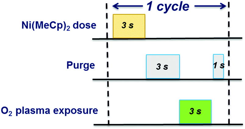 | ||
| Fig. 1 Schematic of the standard recipe used for plasma-assisted ALD of NiO. | ||
Material characterization
The thickness and optical properties of ALD NiO films deposited on c-Si substrates are determined by spectroscopic ellipsometry (SE) (NIR Ellipsometer M2000, J.A. Woollam Co.). The ellipsometric spectra are recorded after every ten ALD cycles over a wavelength range of 275–1600 nm. Two Tauc–Lorentz oscillators are adopted to model the NiO films, as reported in the previous work by Lu et al.28 The thickness and optical constants of the NiO layer are obtained using the following fitting methodology. First, a Cauchy dispersion equation is utilized in the range of 450 to 1600 nm to extract the thickness, as NiO is transparent in this wavelength range. Using the obtained thickness value, the optical constants of the film are then determined over the entire recorded SE spectra (275–1600 nm) using a B-spline model. A bandgap of ∼3.8 eV21,28,35,44–46 is assumed for this fitting step and an initial value of 2.1 is chosen for the refractive index (obtained from the Cauchy dispersion model at the largest wavelength of 1600 nm). Thereafter, the optical constants are parameterized using two Tauc–Lorentz oscillators.28The thickness uniformity is quantified by means of a Woollam ellipsometer M2000 and is determined by dividing the standard deviation (σ) by the average mean NiO thickness.
The crystallinity of the ALD NiO samples is investigated by grazing incidence X-ray diffraction (GI-XRD) using a PANalytical X’Pert Pro MRD system, utilizing Cu Kα radiation (λ = 1.540598 Å) in the 2θ range of 30° to 80° with a step size of 0.05°. XRD of the perovskite films are measured in Bragg–Brentano mode with a step size of 0.013° in the range of 10° to 50°.
Angle-resolved X-ray photoelectron spectroscopy (AR-XPS) is performed to investigate the chemical composition of the ALD NiO films using a Thermo Scientific KA1066 spectrometer. Monochromatic Al Kα X-rays having an energy of 1486.6 eV is utilized and the measurements are performed without any pre-sputtering.
Contact angle is measured with Dataphysics OCA 15plus and analyzed with its software. Scanning electron microscopy (SEM) is performed with a Hitachi SEM. S-4100 at 5 kV and 30![[thin space (1/6-em)]](https://www.rsc.org/images/entities/char_2009.gif) 000× magnification. Transmission electron microscopy (TEM) studies are performed using a JEOL ARM 200 probe corrected TEM operated at 200 kV. The system is equipped with a 100 mm2 Centurio SDD EDX detector. Cross-sectional TEM samples of the PSC are prepared using a standard Focused Ion Beam (FIB) lift-out procedure. Molybdenum support grids are used to mount the samples in the transfer step, upon which the final thinning is performed.
000× magnification. Transmission electron microscopy (TEM) studies are performed using a JEOL ARM 200 probe corrected TEM operated at 200 kV. The system is equipped with a 100 mm2 Centurio SDD EDX detector. Cross-sectional TEM samples of the PSC are prepared using a standard Focused Ion Beam (FIB) lift-out procedure. Molybdenum support grids are used to mount the samples in the transfer step, upon which the final thinning is performed.
Ultraviolet photoelectron spectroscopy (UPS) measurements are performed in a multichamber VG EscaLab II system (Thermo Fisher Scientific Inc.) with a base pressure of ∼10−8 Pa, using He–I radiation (21.2 eV) generated in a differentially pumped discharge lamp while applying −6 V bias to the sample.
Time-resolved photoluminescence (TRPL) measurements are performed using an in-house built system. A 635 nm pulsed laser operating at 5 MHz is used, which incidents from the glass side of the perovskite/ALD NiO/ITO/glass samples.
For the electrochemical impedance spectroscopy (EIS) measurements, 10 nm films of ALD NiO deposited on fluorine doped tin oxide (FTO)/glass substrates are used as the working electrode, along with a Ag/AgCl reference electrode and a platinum mesh counter electrode.22 The electrolyte solution is aqueous 1 M Na2SO4, 0.1 M monobasic sodium phosphate, and is adjusted to pH 12 by dropwise addition of NaOH solution. The area of NiO in contact with the solution is 0.86 cm2. During the measurements, a sinusoidal 10 mV perturbation of selected frequencies is applied at each bias voltage.
Perovskite solar cell fabrication
The fabricated PSCs have an inverted (p–i–n) planar structure and a layer configuration of glass substrate/ITO/ALD NiO/perovskite (Cs0.05(MA0.17FA0.83)Pb1.1(I0.83Br0.17)3)/C60/BCP (bathocuproine)/Cu. 10 nm ALD NiO layers are deposited on top of the ITO coated glass substrates. Thereafter, the NiO coated ITO substrates are annealed in air at 300 °C for 20 min. All the perovskite layer deposition steps are carried out in N2 atmosphere. The perovskite layer is spin-coated using a one-step solution process (4000 rpm for 35 s) following the triple cation procedure.8 25 s after the start of spinning, the ethyl acetate anti-solvent drop (400 μl) is utilized. The films are annealed at 100 °C for 1 h. Afterwards, 23 nm C60 (Sigma Aldrich, purity = 99.9%) is thermally evaporated at a rate of 0.15 Å s−1 at 400 °C. The evaporation of C60 is followed by evaporation of 8 nm BCP. The cells are finished by evaporating 100 nm Cu through a shadow mask. The final active area is 0.16 cm2.Perovskite solar cell characterization
The current density–voltage (J–V) measurements are performed under standard test conditions (25°C, LED sun simulator, Wavelabs, class AAA), adjusted with a calibrated Si reference cell (Fraunhofer ISE). The scan rate is 0.25 V s−1 with a voltage step of 0.02 V. The external quantum efficiency (EQE) is measured as a function of wavelength from 300 to 850 nm with a step of 10 nm using Oriel Instrument's QEPVSI-b system with 300 W xenon arc lamp, controlled by TracQ-Basic software.
Results and discussion
ALD NiO film growth
Fig. 2a–d show the saturation curves for the dose and purge steps of the Ni(MeCp)2 and O2 plasma. The self-limiting saturated growth behavior is confirmed for the ALD NiO process at a deposition temperature of 150 °C. For the precursor saturation curve (Fig. 2a), the O2 plasma exposure time is fixed at 3 s while varying the precursor dosing time. For the O2 plasma saturation curve (Fig. 2c), the precursor dosing time is fixed at 3 s while varying the O2 plasma exposure. ALD saturating behavior is observed for both precursor and O2 plasma half-cycles at an exposure time of 3 s. Meanwhile, negligible variation in GPC is observed with the precursor and O2 plasma purging times (Fig. 2b and d). Fig. 2e shows the thickness of NiO films as a function of number of ALD cycles, as-determined by in situ SE. As seen, the thickness increases linearly with the number of ALD cycles without experiencing any nucleation delay. The GPC in terms of thickness of the ALD NiO films for the investigated deposition temperatures of 50, 100, 150, 200, and 300 °C is shown in Fig. 2f. It is evident that the GPC decreases significantly from ∼0.44 Å at 50 °C to ∼0.32 Å at 150 °C, and then stabilizes at ∼0.32 Å for higher temperatures. The decrease in GPC with increasing deposition temperature could be due to reduction of –OH surface reactive groups due to thermally activated dehydroxylation reaction, and/or could result from densification of the material at higher deposition temperatures.47–51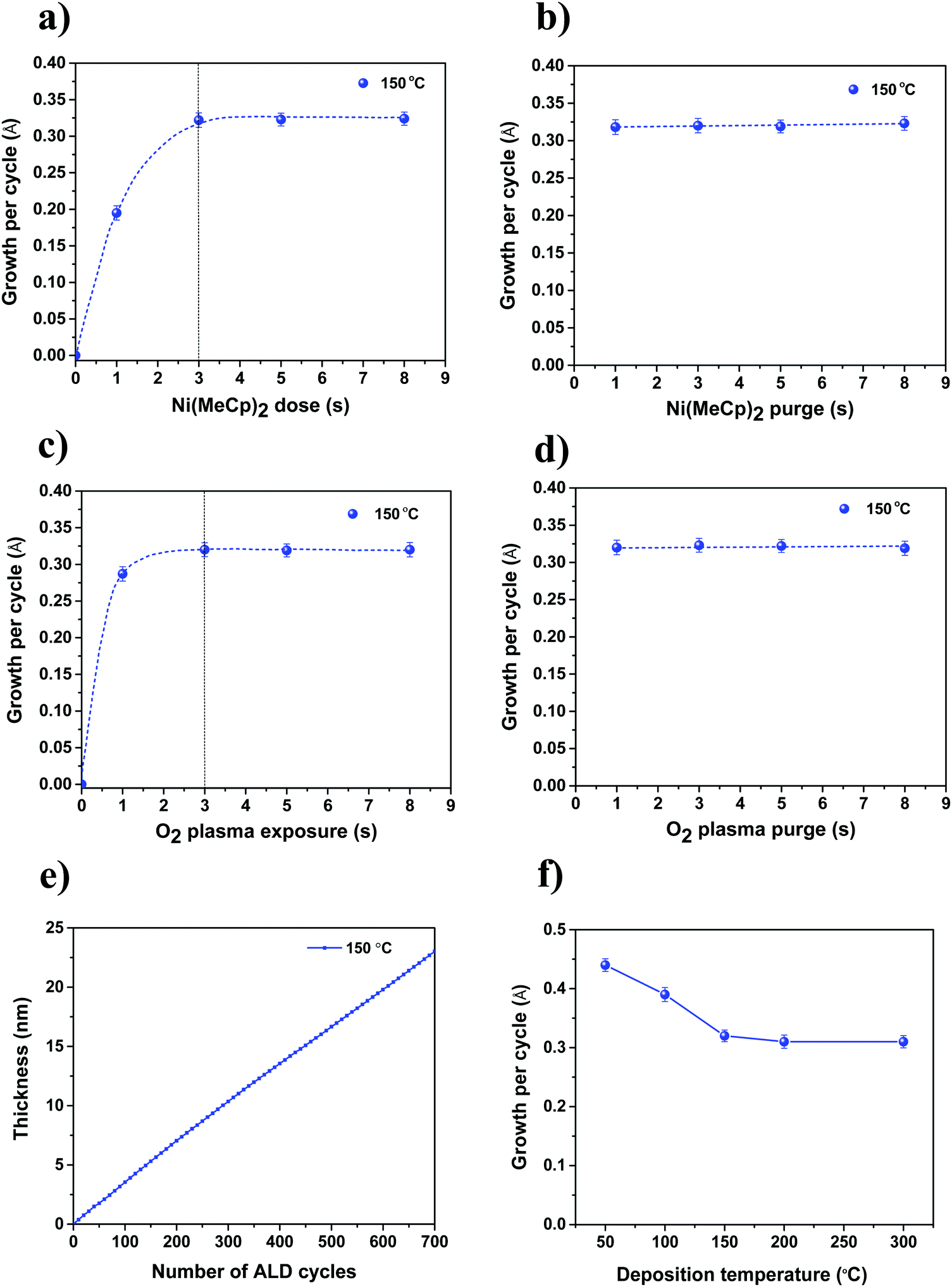 | ||
| Fig. 2 Saturation curves: GPC as a function of (a) precursor Ni(MeCp)2 dosing, (b) Ni(MeCp)2 purge, (c) O2 plasma exposure, and (d) O2 plasma purge for deposition temperature of 150 °C. The dashed lines serve as guide to the eye. (e) NiO film thickness as a function of number of ALD cycles. (f) GPC of NiO in terms of thickness for the investigated deposition temperatures. | ||
Fig. 3 shows the thickness uniformity of the ALD NiO film on a 4 in (100 mm) c-Si wafer, evaluated by mapping its thickness over the whole wafer area by SE at room temperature. 700 ALD cycles are performed at 150 °C on the c-Si wafer with a corresponding GPC of ∼0.32 Å. The thickness non-uniformity is deduced to be less than 0.16%. A good thickness uniformity points out that the plasma-assisted ALD NiO process developed in this work could be utilized for growing these films on large area substrates.
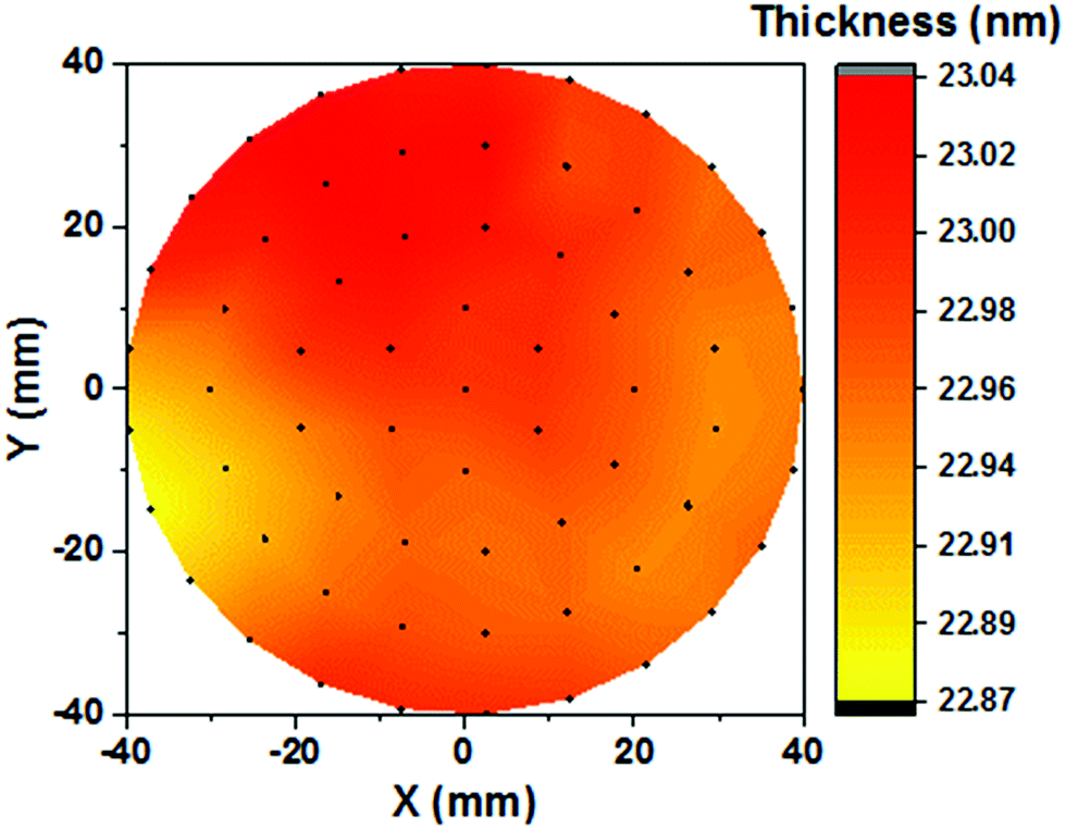 | ||
| Fig. 3 Thickness uniformity of the ALD NiO film deposited at 150 °C on a 4 in (100 mm) c-Si wafer, as-determined by room temperature SE mapping. | ||
Structural and optical characterization of ALD NiO
To characterize the degree of crystallinity of the as-deposited ALD NiO films, surface-sensitive GI-XRD measurement is performed, and the spectrum is shown in Fig. 4a. A face-centered cubic structure is demonstrated by the ALD NiO films as evidenced by the diffraction peaks located at 37.18°, 43.23°, 62.92°, 75.15°, which can be assigned to the (111), (200), (220) and (311) planes, respectively. The diffraction peaks ascribed to pure crystalline nickel, Ni(OH)2, and Ni2O3 phases are absent in the XRD spectrum of Fig. 4a.46,52 The XRD results are in agreement with the earlier reports for NiO films deposited via solution processes,52 sputtering,16 electron-beam-evaporation,46 and by ALD (for processes employing different precursor and co-reactant).22,35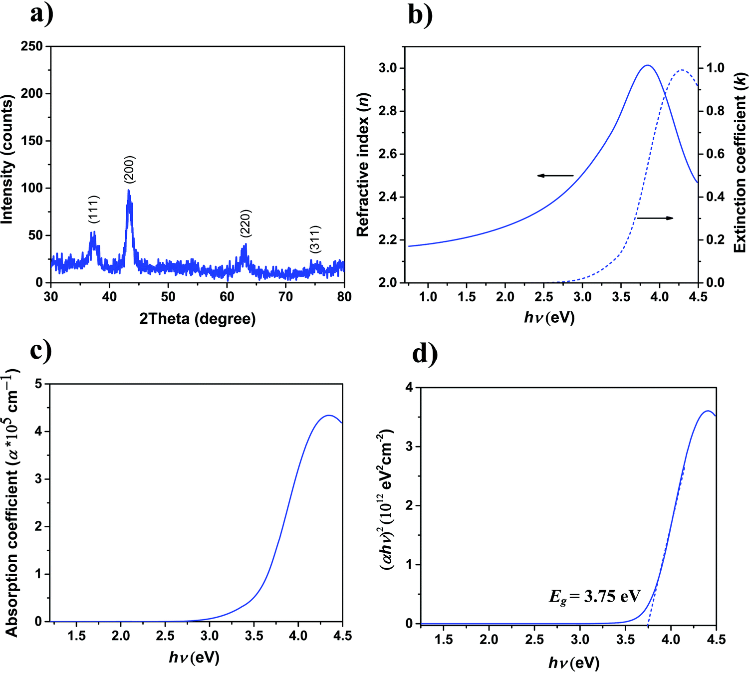 | ||
| Fig. 4 (a) GI-XRD spectrum of an as-deposited 10 nm ALD NiO film, (b) refractive index (n) and extinction coefficient (k) spectra, (c) absorption coefficient (α) spectrum and (d) plot of (αhν)2vs. hν for a 23 nm ALD NiO film deposited on a Si substrate. | ||
The refractive index (n) and extinction coefficient (k) values of 23 nm pristine ALD NiO films extracted from SE are presented in Fig. 4b. The energy dependence of n and k is in agreement with those reported for NiO single crystal53 and films.28,54 The absorption coefficient (α) is presented in Fig. 4c, demonstrating that the deposited NiO film is highly transparent in the investigated spectral range. Considering a direct optical transition in NiO as per literature,16,35,46i.e., r = 2 in the Tauc relation (αhν) = A(hν − Eg)1/r, the variation of (αhν)2versus hν is plotted in Fig. 4d. The band gap (Eg) value is determined from the energy intercept by extrapolating the linear portion of the plot to α = 0. The Eg for ALD NiO film is extracted to be 3.75 eV, which is in good agreement with the values reported in the literature.21,28,35,44–46
ALD NiO as HTL in PSCs
Having analyzed the structural and optical properties of the fabricated ALD films, the work then focusses on the implementation of NiO as HTL in PSCs. Fig. 5a presents a high-angle annular dark field (HAADF) STEM image of the cross-section of the complete planar PSC which consists of glass/ITO/pristine ALD NiO/Perovskite/C60/BCP/Cu. In this stack, ITO serves as front electrode, ALD NiO as HTL, a “triple cation” Cs0.05(MA0.17FA0.83)Pb1.1(I0.83Br0.17)3 perovskite as photo-absorber layer, C60 and BCP together as electron transport layers and Cu as the back electrode. A high-resolution cross-sectional TEM image displaying the ITO/NiO/perovskite interface is shown in Fig. 5b, where a 10 nm conformal NiO layer with excellent thickness homogeneity is clearly distinguishable from the adjacent ITO and perovskite layer. In addition, EDX elemental mappings are acquired at the PSC region depicted in Fig. 5c and the associated elements comprising of Ni (Fig. 5d) and I, Br, Pb, In, O and Cu are shown in Fig. S1(a)–(f) (ESI†).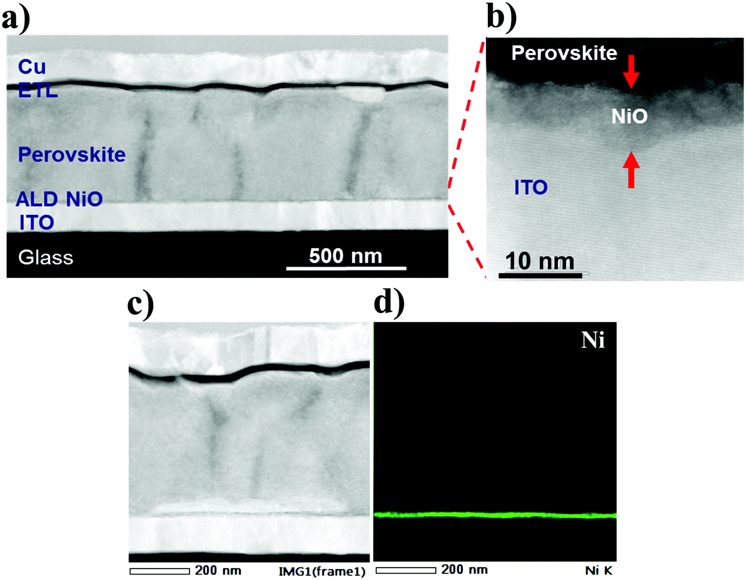 | ||
| Fig. 5 Cross-sectional high angle annular dark field (HAADF) scanning TEM images (a) of the perovskite device stack, (b) of the perovskite/ALD NiO/ITO interface. (d) Elemental map of Ni acquired at the PSC region depicted in (c). | ||
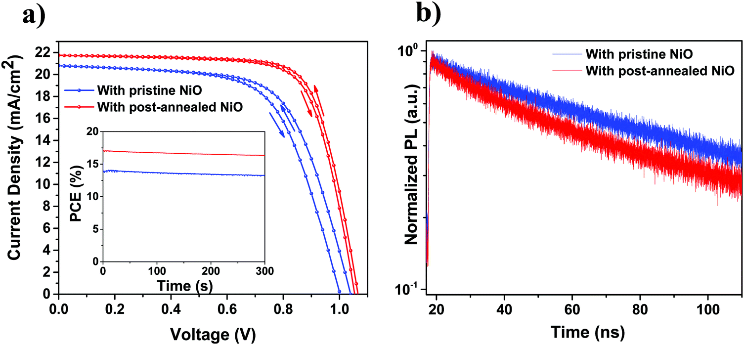
Fig. 6a presents the J–V scans of the PSCs with ALD NiO as HTL. It is observed that “key” to efficient solar cell performance is the post-annealing treatment of the ALD NiO films in air at 300 °C for 20 min, prior to perovskite synthesis. A superior 17.07% PCE is demonstrated in the post-annealed NiO-based device when compared to the 13.98% PCE derived from the one with pristine NiO. This enhancement arises from an increase in short-circuit current density (Jsc) and fill factor (FF), which indicates better light harvesting and hole extraction at the perovskite/post-annealed NiO interface. The increase in Jsc is also corroborated by the EQE spectra measured for both the investigated stacks (Fig. S2, ESI†). The stabilized maximum power point (MPP) tracking results are shown in the inset of Fig. 6a and the PV parameters are summarized in Table 2. The performance of the PSCs has been reproduced for seven tested batches and the statistics of the PV parameters is demonstrated in Fig. S3 (ESI†). It is observed that the slope of J–V curve at the Voc region becomes steeper in the annealed NiO devices. It is well-known that solar cells with a lower series resistance (Rs) exhibit J–V curves with a steeper slope in the Voc region. For the cell with pristine NiO, the value of the Rs is 12.3 Ω cm2 and for the post-annealed NiO device it is 7.8 Ω cm2. This difference in Rs could arise due to different charge extraction at the NiO/perovskite interface with respect to the post-annealing treatment of NiO.
 | ||
| Fig. 6 (a) Forward and backward scanned J–V curves of the champion perovskite devices with pristine and post-annealed ALD NiO as HTLs. Inset shows MPP tracking for 5 min of both the devices. (b) TRPL spectra of glass/ITO/ALD NiO/perovskite samples comparing both the investigated NiO cases. | ||
| Condition | Scan direction | V oc (V) | J sc (mA cm−2) | FF (%) | PCE (%) |
|---|---|---|---|---|---|
| With pristine ALD NiO | Backward | 1.04 | 20.80 | 64.67 | 13.98 |
| Forward | 1.0 | 20.80 | 63.36 | 13.18 | |
| With post-annealed ALD NiO | Backward | 1.07 | 21.75 | 73.36 | 17.07 |
| Forward | 1.05 | 21.75 | 72.42 | 16.54 | |
The difference in charge extraction can be analyzed by PL measurements. TRPL spectra of the perovskite films deposited on ITO/pristine NiO and ITO/post-annealed NiO substrates are presented in Fig. 6b. Considering that both perovskite layers have the same thickness (as confirmed from TEM analysis), charge collection can be differentiated based on the perovskite/NiO interface status. A comparatively faster decay of the charge lifetime is observed for the perovskite deposited on the post-annealed NiO when compared to its counterpart grown atop pristine NiO. It is widely interpreted that a faster decay of the carrier lifetime is an indication of a more efficient charge extraction from the perovskite to the CTLs.55,56 The PL results strongly support the higher PCEs achieved in the post-annealed NiO devices. Alongside the improvement in PCE, it is remarkable to see that the devices with post-annealed ALD NiO experience a reduction in hysteresis (Fig. 6a). This points out that the hysteresis loss in PSCs can be mitigated by careful optimization of the interfaces. To date, the highest PCE of planar PSCs utilizing ALD NiO as HTL is 17.22%.23 The PCE obtained in this work is in line with the efficiencies that have been demonstrated for planar p–i–n PSCs based on undoped NiO HTLs, either processed by ALD21–23 or by other vacuum9,16,46 and solution-based techniques.9,57–59
ALD NiO and perovskite bulk analysis
To understand why post-annealed NiO leads to better device performance, XRD is performed to investigate whether any bulk changes occur in NiO and NiO/perovskite samples with respect to the annealing treatment. As seen in Fig. 7a, no change in crystallinity of ALD NiO is discerned by comparing the XRD spectrum of the films before and after annealing. In parallel, XRD analysis reveals no change in the crystallinity and morphology of the perovskite films grown on top of pristine and post-annealed NiO substrates (Fig. 7b). The results are corroborated by top-view SEM images of the perovskite films, showing no variation in the obtained morphology and a good crystallization quality on top of both the investigated NiO substrates (Fig. 7c and d).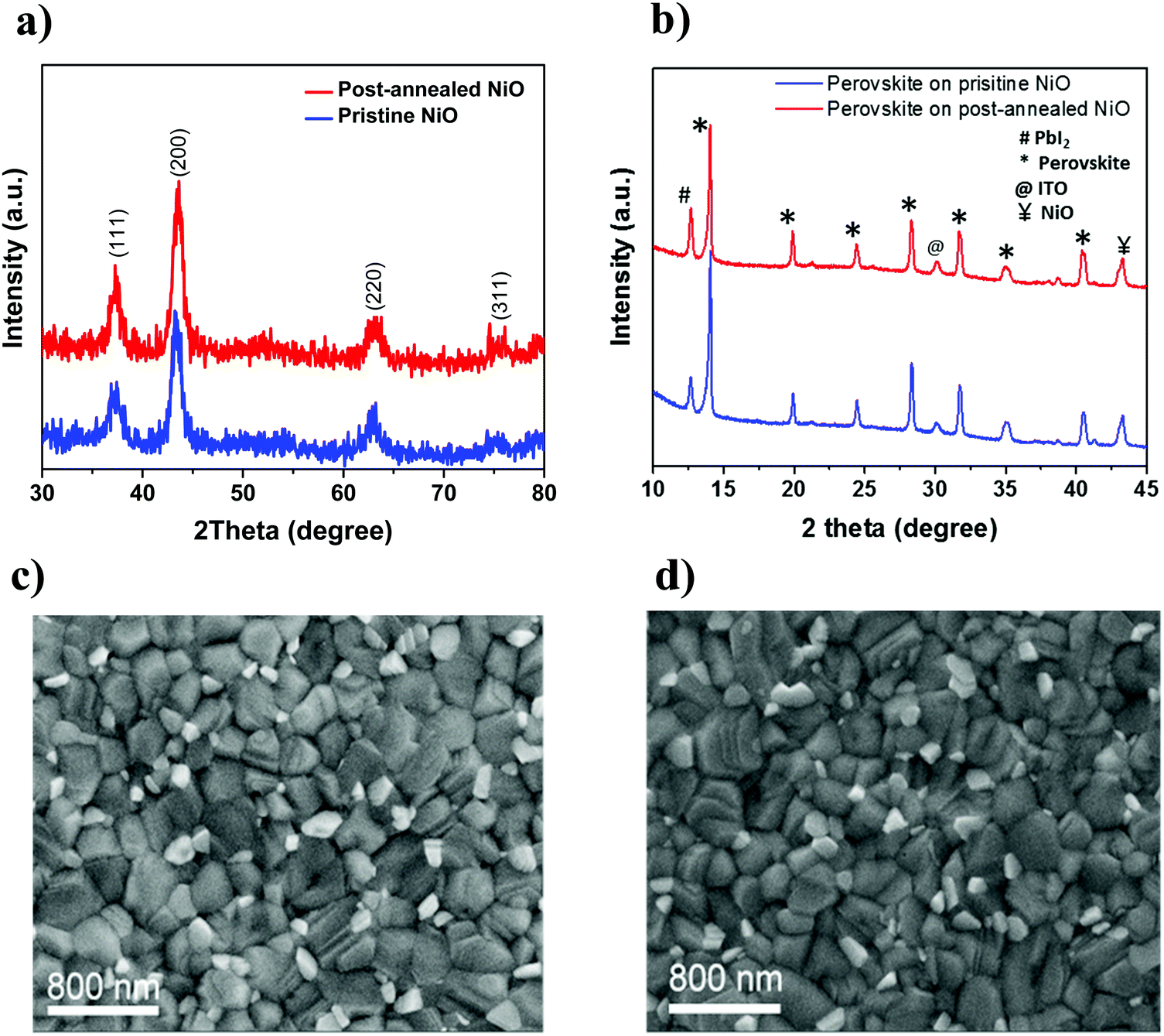 | ||
| Fig. 7 (a) XRD spectra of the ALD NiO film before and after post-annealing at 300 °C in air for 20 min. (b) XRD spectra and top-view SEM images of the perovskite films deposited on top of (c) pristine and (d) post-annealed ALD NiO. | ||
ALD NiO/perovskite interface analysis
Since the bulk properties of both NiO and perovskite films show no difference with respect to the annealing treatment, we then proceed with the analysis of the interface between the perovskite and the ALD NiO layer. First, AR-XPS measurements are performed on pristine NiO films with photoelectron take-off angles (θ) of 90° and 15°. The results confirm that the concentration of hydroxyl species is higher at the surface of NiO (Fig. S4, ESI†). Next, any subtle changes after post-annealing the NiO films are detected by performing XPS with θ of 15°. Fig. 8a and b presents the Ni 2p3/2 and O 1s XPS spectra with pristine (bottom frame) and post-annealed (top frame) ALD NiO films, respectively. We acknowledge that the exact assignment of the Ni 2p3/2 spectra to specific chemical environments is non-trivial, as it is well-known that XPS analysis for the first row transition metals and their oxides and hydroxides is quite challenging due to the complexity of their 2p spectra, primarily arising from peak asymmetries, complex multiplet splitting, overlapping binding energies and shake-up phenomena.22,29,60 However, following the assignments reported in literature,22,29,61–64 the peak at 854 eV (Fig. 8a) is ascribed to the oxidation state of Ni2+, which corresponds to NiO6 octahedral bonding in the cubic rock-salt NiO structure. The second peak at 855.8 eV is attributed to Ni3+ comprising of NiOOH. The broad peaks located at 860 eV and 864 eV are related to shakeup processes (satellites) of NiO. Upon annealing the NiO films, the integrated area of Ni3+ peak decreases, indicating a decrease in the concentration of NiOOH species. The binding energy of the O 1s spectra (Fig. 8b) is mainly resolved into three oxygen states.22,29,61 The peak at 529.4 eV is ascribed to O bonded as Ni–O–Ni. The peaks at 531.1 eV and 532.9 eV are assigned to O bonded as Ni–OH and adsorbed water, respectively. When comparing the O 1s spectra of pristine and post-annealed films, it can be concluded that post-annealing leads to the elimination of hydroxyl groups and adsorbed water from the surface of ALD NiO. The Ni–OH/NiO ratio changes from 1.13 in the pristine to 0.76 in the annealed film.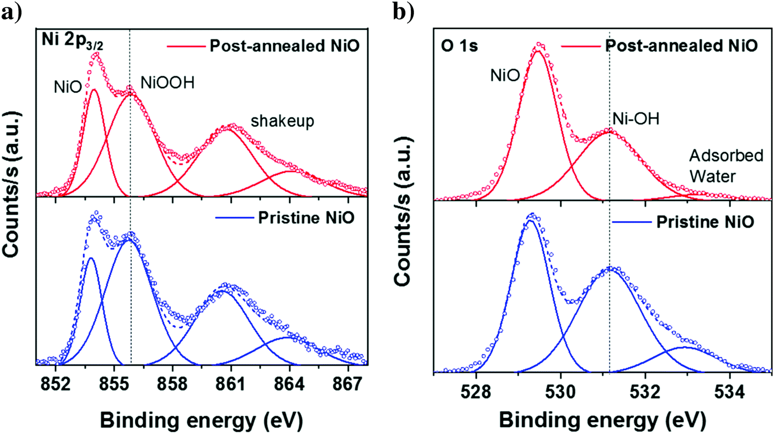 | ||
| Fig. 8 XPS surface spectra of (a) Ni 2p3/2 and (b) O 1s of the pristine (bottom frame) and post-annealed (top frame) ALD NiO films. Open circles, solid lines and dashed lines are measured data, peak fits and cumulative fits, respectively. | ||
In order to gain insights into whether the reduction of surface hydroxyl groups and adsorbed water has any influence on the perovskite/NiO interface quality, contact angle measurements are performed by drop-casting the perovskite precursor solution on top of the two investigated NiO surfaces. A reduction in the contact angle with respect to the post-annealing treatment is clearly evident when comparing the images in Fig. 9a and b, indicating better wetting of perovskite precursor solution on top of post-annealed NiO in comparison to the pristine film. The contact angle measurements confirm that post-annealing indeed changes the surface chemistry of ALD NiO (which is in agreement with our previous XPS analysis), leading to better interfacial properties with the adjacent perovskite layer. We expect that better wetting of the perovskite precursor solution on top of post-annealed NiO could lead to improved performance in the fabricated solar cells.
 | ||
| Fig. 9 Photographs of the contact angle measurements performed on the pristine and post-annealed ALD NiO samples. | ||
Next, we analyze whether post-annealing affects also the energy band alignment of ALD NiO with the perovskite. UPS investigation allows to extract the valence band maximum (VBM) and ionization energy (IE) values for the pristine, post-annealed NiO films and also for the employed triple-cation perovskite layer. More details on UPS data analysis can be found in the ESI† (Fig. S5). Fig. 10a and b shows the UPS spectra of the NiO films deposited on ITO substrates. A VBM of 0.68 eV and an IE of 5.46 eV are measured for the pristine ALD NiO sample. For the post-annealed NiO, a VBM of 0.63 eV and an IE of 5.3 eV are obtained. The perovskite film shows an IE of 6.05 eV and VBM of 1.67 eV (Fig. S6, ESI†). The obtained values are in the range with those reported for mixed-cation perovskite65–67 and also for NiO deposited by different techniques.16,22,68,69 Based on UPS analysis, the energy band diagram of ALD NiO is sketched in Fig. 10c, with the band gap value of NiO being inferred by SE. When comparing the values of IE and VBM for the pristine and post-annealed NiO, it can be observed that the differences are minimal. This indicates that the Voc in the two investigated devices should hardly be influenced, which is in good agreement with our obtained J–V results (Table 2).
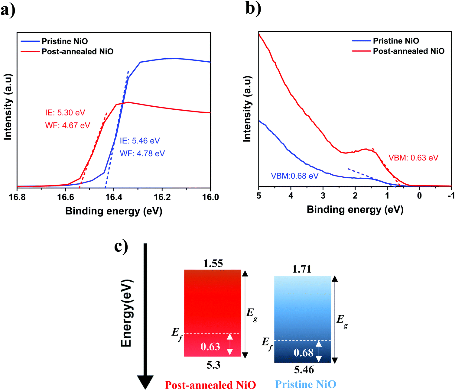 | ||
| Fig. 10 (a and b) UPS spectra of 10 nm ALD NiO film (pristine and post-annealed). (c) Corresponding energy band diagram (in eV) with respect to vacuum level. | ||
A decrease in resistivity of the NiO films from 8.7 × 10² Ω cm to 1.7 × 10² Ω cm is observed after post-annealing, which can explain the decrease in Rs when comparing the corresponding PSCs. Resistivity is dependent on both carrier concentration and mobility of the films. Therefore, to assess whether there is a change in carrier concentration of the ALD NiO films after post-annealing, EIS is performed. Fig. 11 shows the Mott–Schottky plots of the two investigated NiO samples. The results reveal that post-annealing reduces the NiO carrier concentration in the films, from a pristine density of (1.2 ± 0.3) × 1020 cm−3 to (3.5 ± 0.5) × 1019 cm−3. This decrease in carrier concentration is accompanied by an increase in mobility of the NiO films from 6.0 × 10⁻⁵ cm2 V−1 s−1 to 1.0 × 10⁻³ cm2 V−1 s−1, an effect that has been previously reported in the literature.70 The mobility and resistivity of our post-annealed NiO films are in good agreement with the values obtained for spatial-ALD NiO in the recent work of Zhao et al., where these films were utilized as HTL in PSCs.21 Our data support the evidence of higher Jsc and FF in the post-annealed ALD NiO-based devices, and thereby, higher PCEs in comparison to the cells with pristine NiO.
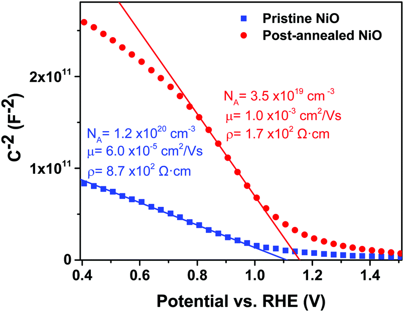 | ||
| Fig. 11 Mott–Schottky plots of pristine and post-annealed ALD NiO samples, at 14 kHz applied frequency. The legend shows the carrier concentration (NA) determined from the slope of the curve using the Mott–Schottky equation, resistivity (ρ) from four point probe measurements, and hole mobility (μ) from 1/ρ = qμNA, where q is the elementary charge. | ||
Conclusions
In summary, a plasma-assisted ALD process capable of producing high-quality thin films of NiO has been developed using Ni(MeCp)2 as precursor and O2 plasma as co-reactant within a table temperature range of 50–300 °C. A linear growth behavior with a growth rate of 0.32 Å per cycle is obtained at 150 °C. The formation of polycrystalline, cubic NiO films with a Eg of 3.75 eV is demonstrated, with excellent thickness uniformity on a 4 inch c-Si wafer. By implementing 10 nm conformal ALD NiO as HTL, efficient p–i–n PSCs are achieved based on triple cation perovskite. It is seen that post-annealing the ALD NiO layers delivers a superior PSC performance with 17.07% PCE when compared to the pristine NiO-based device with 13.98% PCE. In particular, the enhancement in PCE arises from an improved Jsc and FF in the post-annealed NiO devices. The higher Jsc and FF are the result of better hole extraction at the post-annealed HTL/perovskite interface, attributed to better wetting of the perovskite layer atop and increased conductivity and mobility of the NiO films after annealing. Meanwhile, both devices deliver similar Voc as confirmed by UPS analysis, showing negligible change in IE of the NiO films with respect to the annealing treatment. Our work elucidates that a careful design and optimization of the interface between perovskite and ALD NiO holds utmost importance, in addition to the superior bulk properties of the HTL itself, in order to effectively extract the holes and achieve efficient device performance. The choice of adopting ALD as a processing technique can aid in maximizing the surface coverage of the grown CTLs (especially on rough surfaces), thereby mitigating the shunting pathways as well as parasitic absorption losses in PSCs. In addition, suitability of ALD for large-area processing can contribute toward upscaling of perovskite PV technology.Conflicts of interest
The authors declare no competing financial interest.Acknowledgements
We acknowledge Dr Beatriz Barcones Campo for the FIB preparation of the TEM sample, Kseniia Korzun for the PL measurements, Yi Shu from Oxford Instruments for thickness uniformity measurements, Cristian van Helvoirt, Caspar van Bommel and Jeroen van Gerwen for the technical assistance. We are thankful to Dr Yinghuan Kuang, Valerio Di Palma and Dr Anna Todinova for the scientific discussions. Solliance is acknowledged for funding the TEM facility. We are grateful to the financial support from the Light Management in New Photovoltaic Materials (LMPV) research program of the Netherlands Organization for Scientific Research (NWO), from the Dutch Ministry of Economic Affairs, via The Top-consortia Knowledge and Innovation (TKI) Program “High-Efficiency Hybrid Tandem Solar Cells” (HIEFF) (TEZ0214010), “High-Efficiency Si Perovskite Tandem Solar Cells (HIPER)” (TEUE116193) and “ALD for hybrid perovskite solar cells (ALD4PSC)” (TKITOE1409105). M. Jošt and S. Albrecht acknowledge the funding by the German Federal Ministry of Education and Research (BMBF) via program “Materialforschung fuer die Energiewende” (grant no. 03SF0540).References
- NREL. Best Research-Cell Efficiencies http://www.nrel.gov/ncpv/images/efficiency_chart.jpg (accessed May 23, 2019).
- A. Fakharuddin, L. Schmidt-Mende, G. Garcia-Belmonte, R. Jose and I. Mora-Sero, Adv. Energy Mater., 2017, 7, 1700623 CrossRef.
- P. Schulz, D. Cahen and A. Kahn, Chem. Rev., 2019, 119, 3349–3417 CrossRef CAS PubMed.
- C.-G. Wu, C.-H. Chiang, Z.-L. Tseng, M. K. Nazeeruddin, A. Hagfeldt and M. Grätzel, Energy Environ. Sci., 2015, 8, 2725–2733 RSC.
- T. Liu, K. Chen, Q. Hu, R. Zhu and Q. Gong, Adv. Energy Mater., 2016, 6, 1600457 CrossRef.
- B. Chen, Y. Bai, Z. Yu, T. Li, X. Zheng, Q. Dong, L. Shen, M. Boccard, A. Gruverman, Z. Holman and J. Huang, Adv. Energy Mater., 2016, 6, 1601128 CrossRef.
- K. A. Bush, A. F. Palmstrom, Z. J. Yu, M. Boccard, R. Cheacharoen, J. P. Mailoa, D. P. McMeekin, R. L. Z. Hoye, C. D. Bailie, T. Leijtens, I. M. Peters, M. C. Minichetti, N. Rolston, R. Prasanna, S. Sofia, D. Harwood, W. Ma, F. Moghadam, H. J. Snaith, T. Buonassisi, Z. C. Holman, S. F. Bent and M. D. McGehee, Nat. Energy, 2017, 2, 17009 CrossRef CAS.
- M. Jošt, T. Bertram, D. Koushik, J. A. Marquez, M. A. Verheijen, M. D. Heinemann, E. Köhnen, A. Al-Ashouri, S. Braunger, F. Lang, B. Rech, T. Unold, M. Creatore, I. Lauermann, C. A. Kaufmann, R. Schlatmann and S. Albrecht, ACS Energy Lett., 2019, 4, 583–590 CrossRef.
- J. Chen and N.-G. Park, J. Phys. Chem. C, 2018, 122, 14039–14063 CrossRef CAS.
- Y. Wang, R. Wenisch, R. Schlatmann and I. Lauermann, Adv. Energy Mater., 2018, 8, 1801692 CrossRef.
- F. Sahli, J. Werner, B. A. Kamino, M. Bräuninger, R. Monnard, B. Paviet-Salomon, L. Barraud, L. Ding, J. J. Diaz Leon, D. Sacchetto, G. Cattaneo, M. Despeisse, M. Boccard, S. Nicolay, Q. Jeangros, B. Niesen and C. Ballif, Nat. Mater., 2018, 17, 820–826 CrossRef CAS PubMed.
- Z. Jehl, M. Bouttemy, D. Lincot, J. F. Guillemoles, I. Gerard, A. Etcheberry, G. Voorwinden, M. Powalla and N. Naghavi, J. Appl. Phys., 2012, 111, 114509 CrossRef.
- S. Sajid, A. M. Elseman, H. Huang, J. Ji, S. Dou, H. Jiang, X. Liu, D. Wei, P. Cui and M. Li, Nano Energy, 2018, 51, 408–424 CrossRef CAS.
- J. Burschka, N. Pellet, S.-J. Moon, R. Humphry-Baker, P. Gao, M. K. Nazeeruddin and M. Grätzel, Nature, 2013, 499, 316 CrossRef CAS PubMed.
- Z. Qiu, H. Gong, G. Zheng, S. Yuan, H. Zhang, X. Zhu, H. Zhou and B. Cao, J. Mater. Chem. C, 2017, 5, 7084–7094 RSC.
- E. Aydin, J. Troughton, M. De Bastiani, E. Ugur, M. Sajjad, A. Alzahrani, M. Neophytou, U. Schwingenschlögl, F. Laquai, D. Baran and S. De Wolf, ACS Appl. Energy Mater., 2018, 1, 6227–6233 CrossRef.
- J. Cui, F. Meng, H. Zhang, K. Cao, H. Yuan, Y. Cheng, F. Huang and M. Wang, ACS Appl. Mater. Interfaces, 2014, 6, 22862–22870 CrossRef CAS PubMed.
- W. Chen, Y. Wu, J. Liu, C. Qin, X. Yang, A. Islam, Y.-B. Cheng and L. Han, Energy Environ. Sci., 2015, 8, 629–640 RSC.
- S. M. George, Chem. Rev., 2010, 110, 111–131 CrossRef CAS PubMed.
- S. E. P. H. C. M. Knoops, A. A. Bol and W. M. M. Kessels, Handbook of Crystal Growth, Elsevier, New York, 2nd edn, 2015, pp. 1101–1134 Search PubMed.
- B. Zhao, L. C. Lee, L. Yang, A. J. Pearson, H. Lu, X.-J. She, L. Cui, K. H. L. Zhang, R. L. Z. Hoye, A. Karani, P. Xu, A. Sadhanala, N. C. Greenham, R. H. Friend, J. L. MacManus-Driscoll and D. Di, ACS Appl. Mater. Interfaces, 2018, 10, 41849–41854 CrossRef CAS PubMed.
- S. Seo, I. J. Park, M. Kim, S. Lee, C. Bae, H. S. Jung, N.-G. Park, J. Y. Kim and H. Shin, Nanoscale, 2016, 8, 11403–11412 RSC.
- S. Seo, S. Jeong, C. Bae, N.-G. Park and H. Shin, Adv. Mater., 2018, 30, 1801010 CrossRef PubMed.
- Y. Zhang, L. Du, X. Liu and Y. Ding, Appl. Surf. Sci., 2019, 481, 138–143 CrossRef CAS.
- C. Guan, Y. Wang, Y. Hu, J. Liu, K. H. Ho, W. Zhao, Z. Fan, Z. Shen, H. Zhang and J. Wang, J. Mater. Chem. A, 2015, 3, 23283–23288 RSC.
- H. L. Lu, G. Scarel, C. Wiemer, M. Perego, S. Spiga, M. Fanciulli and G. Pavia, J. Electrochem. Soc., 2008, 155, H807–H811 CrossRef CAS.
- J. Bachmann, A. Zolotaryov, O. Albrecht, S. Goetze, A. Berger, D. Hesse, D. Novikov and K. Nielsch, Chem. Vap. Deposition, 2011, 17, 177–180 CrossRef CAS.
- H. L. Lu, G. Scarel, M. Alia, M. Fanciulli, S.-J. Ding and D. W. Zhang, Appl. Phys. Lett., 2008, 92, 222907 CrossRef.
- K. L. Nardi, N. Yang, C. F. Dickens, A. L. Strickler and S. F. Bent, Adv. Energy Mater., 2015, 5, 1500412 CrossRef.
- M.-H. Ko, B. Shong and J.-H. Hwang, Ceram. Int., 2018, 44, 16342–16351 CrossRef CAS.
- K. M. H. Young and T. W. Hamann, Chem. Commun., 2014, 50, 8727–8730 RSC.
- E. Thimsen, A. B. F. Martinson, J. W. Elam and M. J. Pellin, J. Phys. Chem. C, 2012, 116, 16830–16840 CrossRef CAS.
- C.-C. Hsu, H.-W. Su, C.-H. Hou, J.-J. Shyue and F.-Y. Tsai, Nanotechnology, 2015, 26, 385201 CrossRef PubMed.
- T. S. Yang, W. Cho, M. Kim, K.-S. An, T.-M. Chung, C. G. Kim and Y. Kim, J. Vac. Sci. Technol., A, 2005, 23, 1238–1243 CrossRef CAS.
- A. G. Hufnagel, A.-K. Henß, R. Hoffmann, O. E. O. Zeman, S. Häringer, D. Fattakhova-Rohlfing and T. Bein, Adv. Mater. Interfaces, 2018, 5, 1701531 CrossRef.
- H. C. M. Knoops, T. Faraz, K. Arts and W. M. M. Kessels, J. Vac. Sci. Technol., A, 2019, 37, 030902 CrossRef.
- S.-H. Ji, W.-S. Jang, J.-W. Son and D.-H. Kim, Korean J. Chem. Eng., 2018, 35, 2474–2479 CrossRef CAS.
- S. J. Song, S. W. Lee, G. H. Kim, J. Y. Seok, K. J. Yoon, J. H. Yoon, C. S. Hwang, J. Gatineau and C. Ko, Chem. Mater., 2012, 24, 4675–4685 CrossRef CAS.
- K. E. K. Holden, C. L. Dezelah and J. F. Conley, ACS Appl. Mater. Interfaces, 2019, 11, 30437–30445 CrossRef CAS PubMed.
- M. Utriainen, M. Kröger-Laukkanen and L. Niinistö, Mater. Sci. Eng., B, 1998, 54, 98–103 CrossRef.
- P. Antony Premkumar, M. Toeller, C. Adelmann, J. Meersschaut, A. Franquet, O. Richard, H. Tielens, B. Brijs, A. Moussa, T. Conard, H. Bender, M. Schaekers, J. A. Kittl, M. Jurczak and S. Van Elshocht, Chem. Vap. Deposition, 2012, 18, 61–69 CrossRef CAS.
- E. Lindahl, M. Ottosson and J.-O. Carlsson, Chem. Vap. Deposition, 2009, 15, 186–191 CrossRef CAS.
- S. B. S. Heil, E. Langereis, F. Roozeboom, M. C. M. van de Sanden and W. M. M. Kessels, J. Electrochem. Soc., 2006, 153, G956–G965 CrossRef CAS.
- D. Adler and J. Feinleib, Phys. Rev. B: Solid State, 1970, 2, 3112–3134 CrossRef.
- H. Kamal, E. K. Elmaghraby, S. A. Ali and K. Abdel-Hady, J. Cryst. Grow., 2004, 262, 424–434 CrossRef CAS.
- T. Abzieher, S. Moghadamzadeh, F. Schackmar, H. Eggers, F. Sutterlüti, A. Farooq, D. Kojda, K. Habicht, R. Schmager, A. Mertens, R. Azmi, L. Klohr, J. A. Schwenzer, M. Hetterich, U. Lemmer, B. S. Richards, M. Powalla and U. W. Paetzold, Adv. Energy Mater., 2019, 9, 1802995 CrossRef.
- E. Langereis, J. Keijmel, M. C. M. van de Sanden and W. M. M. Kessels, Appl. Phys. Lett., 2008, 92, 231904 CrossRef.
- S. E. Potts, W. Keuning, E. Langereis, G. Dingemans, M. C. M. van de Sanden and W. M. M. Kessels, J. Electrochem. Soc., 2010, 157, P66–P74 CrossRef CAS.
- G. Dingemans, M. C. M. van de Sanden and W. M. M. Kessels, Electrochem. Solid-State Lett., 2010, 13, H76–H79 CrossRef CAS.
- G. Dingemans, C. A. A. van Helvoirt, D. Pierreux, W. Keuning and W. M. M. Kessels, J. Electrochem. Soc., 2012, 159, H277–H285 CrossRef CAS.
- S. Balasubramanyam, A. Sharma, V. Vandalon, H. C. M. Knoops, W. M. M. Kessels and A. A. Bol, J. Vac. Sci. Technol., A, 2017, 36, 01B103 CrossRef.
- X. Yin, P. Chen, M. Que, Y. Xing, W. Que, C. Niu and J. Shao, ACS Nano, 2016, 10, 3630–3636 CrossRef CAS PubMed.
- R. J. Powell and W. E. Spicer, Phys. Rev. B: Solid State, 1970, 2, 2182–2193 CrossRef.
- A. M. López-Beltrán and A. Mendoza-Galván, Thin Solid Films, 2006, 503, 40–44 CrossRef.
- G. Xing, N. Mathews, S. Sun, S. S. Lim, Y. M. Lam, M. Grätzel, S. Mhaisalkar and T. C. Sum, Science, 2013, 342, 344 CrossRef CAS PubMed.
- Y. Lee, S. Lee, G. Seo, S. Paek, K. T. Cho, A. J. Huckaba, M. Calizzi, D.-w. Choi, J.-S. Park, D. Lee, H. J. Lee, A. M. Asiri and M. K. Nazeeruddin, Adv. Sci., 2018, 5, 1800130 CrossRef PubMed.
- W. J. Scheideler, N. Rolston, O. Zhao, J. Zhang and R. H. Dauskardt, Adv. Energy Mater., 2019, 1803600 CrossRef.
- T. Wang, D. Ding, H. Zheng, X. Wang, J. Wang, H. Liu and W. Shen, Sol. RRL, 2019, 1900045 CrossRef.
- X. Zhao, J. Chen and N.-G. Park, Sol. RRL, 2019, 3, 1800339 CrossRef.
- A. G. Marrani, V. Novelli, S. Sheehan, D. P. Dowling and D. Dini, ACS Appl. Mater. Interfaces, 2014, 6, 143–152 CrossRef CAS PubMed.
- J. W. Shim, C. Fuentes-Hernandez, A. Dindar, Y. Zhou, T. M. Khan and B. Kippelen, Org. Electron., 2013, 14, 2802–2808 CrossRef CAS.
- M. T. Greiner, M. G. Helander, Z.-B. Wang, W.-M. Tang and Z.-H. Lu, J. Phys. Chem. C, 2010, 114, 19777–19781 CrossRef CAS.
- A. P. Grosvenor, M. C. Biesinger, R. S. C. Smart and N. S. McIntyre, Surf. Sci., 2006, 600, 1771–1779 CrossRef CAS.
- L. Soriano, I. Preda, A. Gutiérrez, S. Palacín, M. Abbate and A. Vollmer, Phys. Rev. B: Condens. Matter Mater. Phys., 2007, 75, 233417 CrossRef.
- H. Tan, A. Jain, O. Voznyy, X. Lan, F. P. García de Arquer, J. Z. Fan, R. Quintero-Bermudez, M. Yuan, B. Zhang, Y. Zhao, F. Fan, P. Li, L. N. Quan, Y. Zhao, Z.-H. Lu, Z. Yang, S. Hoogland and E. H. Sargent, Science, 2017, 355, 722 CrossRef CAS PubMed.
- Y. Kuang, V. Zardetto, R. van Gils, S. Karwal, D. Koushik, M. A. Verheijen, L. E. Black, C. Weijtens, S. Veenstra, R. Andriessen, W. M. M. Kessels and M. Creatore, ACS Appl. Mater. Interfaces, 2018, 10, 30367–30378 CrossRef CAS PubMed.
- J. P. Correa Baena, L. Steier, W. Tress, M. Saliba, S. Neutzner, T. Matsui, F. Giordano, T. J. Jacobsson, A. R. Srimath Kandada, S. M. Zakeeruddin, A. Petrozza, A. Abate, M. K. Nazeeruddin, M. Grätzel and A. Hagfeldt, Energy Environ. Sci., 2015, 8, 2928–2934 RSC.
- S. Yue, K. Liu, R. Xu, M. Li, M. Azam, K. Ren, J. Liu, Y. Sun, Z. Wang, D. Cao, X. Yan, S. Qu, Y. Lei and Z. Wang, Energy Environ. Sci., 2017, 10, 2570–2578 RSC.
- J. Kim, H. J. Park, C. P. Grigoropoulos, D. Lee and J. Jang, Nanoscale, 2016, 8, 17608–17615 RSC.
- S. Han and A. J. Flewitt, Sci. Rep., 2017, 7, 5766 CrossRef PubMed.
Footnote |
| † Electronic supplementary information (ESI) available: Details on UPS data analysis, cross-sectional TEM image of PSC with post-annealed ALD NiO, comparative EQE spectra and box-plot of the PV parameters of pristine and post-annealed NiO-based PSCs, TEM-EDX elemental mappings of I, Br, Pb, In, O and Cu present in the perovskite device stack, AR-XPS spectra of Ni 2p3/2 and O 1s of the pristine NiO film measured with θ of 90° and 15°, UPS spectra of the employed triple cation-based perovskite layer, transmittance spectra of the pristine and post-annealed ALD NiO films. See DOI: 10.1039/c9tc04282b |
| This journal is © The Royal Society of Chemistry 2019 |