
 Open Access Article
 This Open Access Article is licensed under a
 Creative Commons Attribution 3.0 Unported Licence
Novel approaches and scalability prospects of copper based hole transporting materials for planar perovskite solar cells
Maria
Bidikoudi
and
Emmanuel
Kymakis
 *
*
Department of Electrical and Computer Engineering, Hellenic Mediterranean University, Estavromenos, Heraklion 71410, Crete, Greece. E-mail: kymakis@hmu.gr
First published on 26th August 2019
Abstract
A decade after their first appearance as components of solar cells, perovskites are still at the center of solar research. Material and device engineering has led to high PCE values that now surpass 22%. Even though the lion's share is devoted to the development of perovskite structures, which has been crucial for the leap in efficiency values, the charge transport layers – electrons and holes – have a significant effect on the corresponding devices’ performance as well. The determining effect of these layers’ properties is particularly reflected in the stability of devices, especially when moving from lab scale to large scale. For the ability of PSC technology to make a step towards their commercialization, stable and low cost, large area PSCs need to be demonstrated and even though significant advances have been made in demonstrating stable modules and panels, the cost remains an inhibiting factor for potential investments in this field. Among the components of a PSC, the HTL is responsible for a great part of the cost, since the most efficient devices so far incorporate expensive HTMs, such as spiro-OMeTAD and PTAA. The inverted structure PSCs offer a wide range of alternative HTLs, since in this device configuration the HTL is deposited below the easily destructible perovskite layer. Hence, any material with modest hole mobility is a potential alternative for the replacement of the costly HTMs used so far. In this context, we have gathered the most recent works that have been demonstrated, regarding Cu based materials applied as HTMs in planar p-i-n structure PSCs. This family of materials is receiving an increasing amount of interest in the scientific community, owing to their favorable charge transfer properties (e.g. high hole mobility), their physical properties (e.g. solubility in various solvents), their ability to form dense, uniform and smooth films, with numerous methods and most importantly their low cost. We expect that this review, by presenting and discussing the applications of Cu based materials as HTMs in planar PSCs, in a clear and thorough way, will highlight their importance and capabilities in the field and provide a motivation towards their further exploration.
 Maria Bidikoudi | Maria Bidikoudi received her BSc in Physics from the University of Patras in 2009, MSc in Energy from Heriot-Watt University in 2010 and her PhD degree in Chemical Engineering from the National Technical University of Athens in 2016. She has been a Research Assistant in the National Centre for Scientific Research “Demokritos” since 2010, focusing on Dye Sensitized Solar Cells based on ionic liquid electrolytes and other types of Electrochemical Cells. She is currently a Post Doctoral Researcher, member of the NANO Group, focusing on Perovskite Solar Cells, in the Hellenic Mediterranean University, in Crete. |
 Emmanuel Kymakis | Emmanuel Kymakis is a Full Professor at the Department of Electrical & Computer Engineering of the Hellenic Mediterranean University and director of the Center of Materials Technology & Photonics. His research is focused on the realization of advanced materials and solution processable optoelectronic and energy devices for emerging technologies and applications. He is currently the leader of the Energy Generation WP of the FET-Flagship Initiative Graphene, a member of the Engineering sectoral scientific council of the National Council for Research & Innovation of Greece (NCRI) and a member of the Engineering thematic advisory council of HFRI. |
1. Introduction
Organic–inorganic perovskites have completed ten years in the spotlight, after the first report on their implementation in solar cells,1 which has established a new field of research, with continuously growing, highly promising results, at both the material and the consequent device level. With a wide variety of applications in optoelectronics, perovskites have been the most widely studied material in this field after the Si revolution.The advances during the last ten years have been huge: new perovskite structures have emerged,2–4 innovative charge transport layers have been proposed,5–10 novel nanomaterials have been synthesized and used as highly efficient interlayers,11–13 while intensive research on device engineering has led to the realization of large area and tandem devices.14 Finally, Perovskite Solar Cells (PSCs) have also now been demonstrated to be stable for thousands of hours under conditions that should mimic those that a real device can be exposed to.15 However, there are still several drawbacks that hinder their secure penetration into the market, with the most important of these being the device stability under real time operational conditions, the environmental impact of the modules with concerns around lead and tin still being debated, the performance loss when upscaling to large-area devices, and remaining gaps in the fundamental materials physics.16
From the commercialization point of view, the hole transporting material (HTM) utilized in the PSC structure is a key component, since it currently dominates both the performance and cost of the PSC. Organic HTMs, such as 2,2′,7,7′-tetrakis[N,N-di(4-methoxyphenyl)amino]-9,9′-spirobifluorene (spiro-OMeTAD) and poly[bis(4-phenyl)(2,4,6-trimethylphenyl)amine] (PTAA), currently dominate the PSC field, mainly due to their mild processing conditions compatible with perovskites. However, because of their organic nature, these HTMs exhibit relatively low hole mobility and, therefore, they require the presence of chemical dopants to improve their efficiency. The employed additives induce device degradation due to their hygroscopic properties. On top of that, both spiro-OMeTAD and PTAA are highly expensive (the price of spiro-OMeTAD is 23 times and PTAA is 57 times higher than that of gold). Hence, the utilization of low-cost, scalable but also abundant and possibly environmentally sustainable HTMs is highly desired to improve the progress of PSCs towards commercialization.
Copper based inorganic p-type semiconductors, such as copper iodide (CuI), copper thiocyanate (CuSCN) and copper oxide (CuO), have several unique properties, including ease of fabrication correlated with low production cost, suitable band alignment with the perovskite active layer, high hole mobility/conductivity, solution-processability and high chemical stability. These merits make the Cu based p-type semiconductors promising HTM candidate materials that can be explored in PSCs.
In this review, an overview of Cu based HTMs will be presented, with a focus on their implementation in PSCs of the inverted structure. Starting from an introduction to the device configuration of p-i-n PSCs, where the advantages over the normal structure will be highlighted, we move to the demonstration of the most commonly used HTMs and the recent trend in this field. Special attention is paid to the challenges related to the large-scale application of the current state-of-the-art HTMs, which is also a motivation for turning the attention to high mobility Cu derivatives. The scope of this review is (i) to demonstrate the great potential of inverted structure PSCs, regarding their large scale application, from a materials’ point of view, (ii) to provide a clear and thorough illustration of the present status and the novelties of research on Cu derivatives as HTMs in p-i-n structure PSCs and (iii) to constitute a motivation towards further investigation of these materials, by demonstrating their capability for large area, low cost, highly efficient and stable devices.
2. Device architecture, advantages and challenges
2.1 Inverted PSCs: short description, advantages
The first PSC that was reported came as a development of earlier generation solar cells: the dye sensitized solar cells (DSCCs), which have been at the center of research since the early 90s and by 2009 had already reached the commercialization level, being produced by several companies (e.g. GreatCell Solar, G24, H. Glass, Exeger, Solaronix, etc.). The perovskite was used in that cell as the sensitizer, which, combined with a solid state, hole transport medium, such as spiro-OMeTAD, achieved promising efficiency.1 It is no wonder therefore that the first PSCs, and the most widely explored ones, are based on the mesoscopic normal structure (n-i-p). Despite the high power conversion efficiency (PCE) that this structure is able to achieve, their large scale application is inhibited by two factors: the first one is the high temperature demanding oxides, which are mainly used as the electron transport material (ETM), and the second one is the pricey and unstable spiro-OMeTAD that is used as the HTM. These two parameters, combined with the perovskite instability as a material itself, make the upscaling of the devices unfeasible.After the establishment of the bipolar nature of the perovskite, in 2012,17 it was evident that a mesoporous scaffold is not necessary for achieving an operating PSC. Researchers also found that the charge carrier diffusion length was high enough (100 nm for CH3NH3PbI3 and 1 μm for CH3NH3PbI3−xClx)18,19 to ensure efficient charge transport in the perovskite films, thus opening the road towards new device configurations. Based on the organic photovoltaics (OPVs), Jeng et al. developed the first inverted planar heterojunction PSC in 2013.20 In this configuration, the p-type layer was deposited prior to the perovskite film, while the n-type layer was deposited after the perovskite film. This architecture was defined as the p-i-n structure or inverted structure. In the typical inverted, planar structure (p-i-n) the Hole Transport Layer (HTL) is deposited, with the appropriate deposition technique from a starting Hole Transport Material (HTM), on a conductive substrate, typically ITO. The perovskite film is grown on the HTL, on top of which the ETL is deposited. To close the circuit, a low work function metal is evaporated on the ETL (Fig. 1). In this pioneering work, typical OPV materials were introduced into PSCs, which helped to bridge the gap between PSCs and OPVs. Thus, the advantages of OPVs, such as easy fabrication, high throughput, and material diversity, can all be combined into the inverted PSC.21
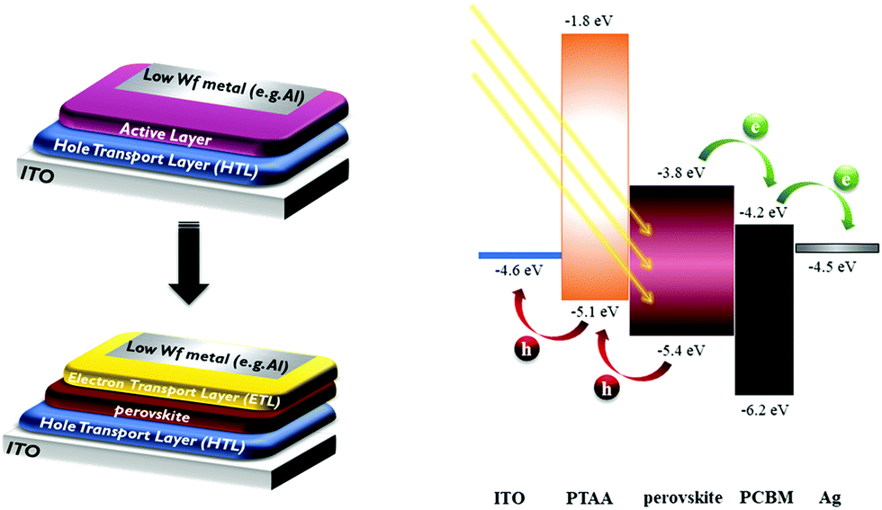 | ||
| Fig. 1 Moving from OPVs to PSCs: device configuration (left) energy level diagram of a typical inverted PSC (right). | ||
2.2 Types of perovskites that have been used; performance and stability of devices
Organometal trihalide perovskite materials have been the first type of perovskite materials to attract considerable research interest for solar cell applications, owing to their many intriguing optical and electronic properties, such as very high absorption coefficient, high charge carrier mobility, long carrier recombination lifetime, and unique defect physics. Benefiting from these excellent properties, the PCE of PSCs has been greatly improved from 3.8%22 to over 20% in their ten years of development. Among the different hybrid organic inorganic perovskites (HOIP) that have been used, methylammonium lead triiodide (CH3NH3PbI3) is the one that has been most intensively investigated. It is characterized by high carrier mobility, excellent absorption coefficient, bandgap tunability, long diffusion length, and low material cost, making it a highly promising material.However, MAPbI3 perovskites rarely reach efficiencies larger than 20% despite the numerous attempts made since the early days of research in the field, while there are serious concerns with respect to their stability, such as the structural phase transition at high temperature and degradation upon contact with moisture. In the case of “mixed halide” perovskites CH3NH3PbBrxI(3−x), thermal stability as well as light-induced trap-state formation and halide segregation also remains a drawback, concerning the stability of devices. The poor stability of CH3NH3Pb-halides severely limits their commercialization potential.
Another widely used perovskite material is CH(NH2)2PbI3 (FAPbI3). Owing to the reduction of symmetry, the bandgap of FAPbI3 is estimated to be 1.48 eV, whereas that of MAPbI3 is 1.52 eV. MAPbI3 and FAPbI3 have been used as light-absorbing layers in devices, where FAPbI3 exhibited higher PCE than the MAPbI3-based device and at the same time it appeared to be fully stable without decomposition at 150 °C in air, whereas MAPbI3 broke down into PbI2 and CH3NH3, indicating that FAPbI3 has higher thermal stability than MAPbI3.23 Despite the several advantages of FAPbI3 over MAPbI3, FAPbI3 has not been studied intensively, mainly due to its instability against humidity.
The instability of black perovskite FAPbI3 is due to the instability of either the black phase or formamidinium itself in the presence of water. Black perovskite FAPbI3 has been reported to convert to the yellow non-perovskite phase in the presence of solvents while the formamidinium cation dissociated to ammonia and sym-triazine in the presence of water, although both were stable under a dry atmosphere. For stabilization of black FAPbI3, the mixed cation and/or halide system of FA1−xMAxPbI3 or FA1−xMAxPbI3−yBry has been suggested.24
One approach to stabilize perovskites is the use of more complex compositions, such as double-cation, double-halide perovskites (using MA, FA or Cs, FA) that show a stable “black phase” at room temperature. These perovskites exhibit unexpected, novel properties; for example, CsFA mixtures suppress halide segregation enabling band gaps for perovskite/silicon or perovskite/perovskite tandems (Fig. 2). The strategy of mixed-cation perovskites has been extended further to triple cation CsMAFA perovskites, which suppress the detrimental yellow phase impurities in highly efficient MAFA compounds, which has been a key insight improvement for enabling reproducible, high quality films that are less sensitive to “hidden” processing parameters (such as environmental temperature and solvent vapours). The triple cation perovskites resulted in a stabilized PCE of 21.1% in 2017 and have been adopted by various groups since.25 Thus, a design for mixing cations and halides in perovskite compounds is necessary to improve the thermal and structural stability (Table 1).
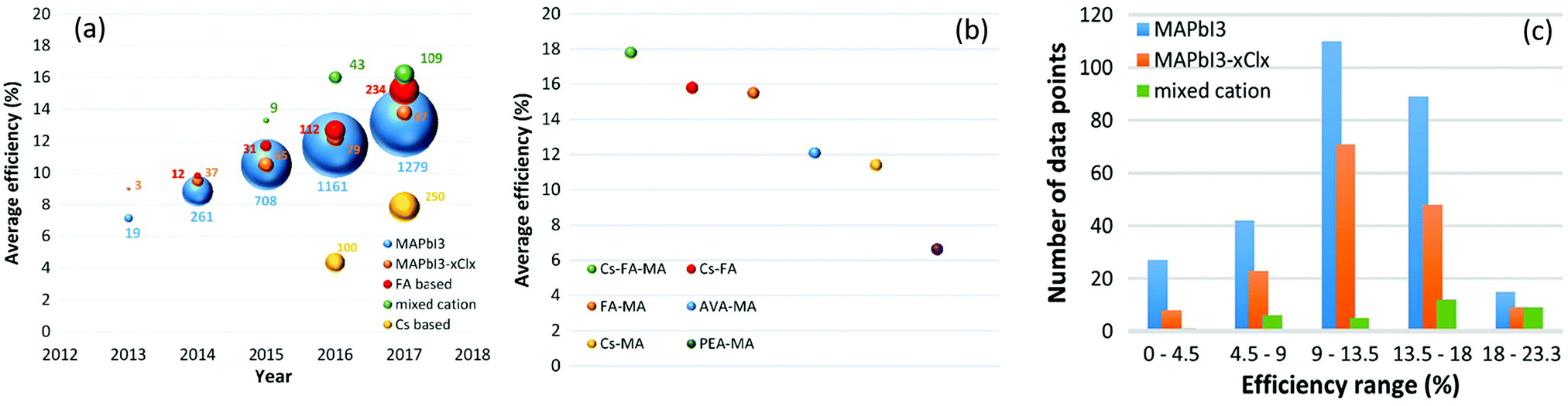 | ||
| Fig. 2 (a) Comparison of number of papers published (ball size) and average efficiencies (y-axis) obtained with various perovskites through years. (b) Comparison of average PCEs of mixed cation perovskites. (c) Distribution of PCE in the database obtained with different common perovskites in an inverted (p-i-n) cell structure.26 | ||
| Perovskite | PCE [%] | HTL | Stability | Ref. |
|---|---|---|---|---|
| MAPbI3 | 20.2 | Poly[(9,9-dioctyl-fluorenyl-2,7-diyl)-co-(4,4′-(N-(4-secbutylphenyl)diphenylamine))] (TFB) | 90% – 30 days | 27 |
| Cs005(FA085MA085)095Pb(I085Br015)3 | 20.7 | Poly[bis(4-phenyl)(2,4,6-trimethylphenyl)amine] (PTAA) | 60% – 7 days | 28 |
| MA0.80FA0.20PbI3−yCly | 18.14 | Poly(3,4-ethylenedioxythiophene):poly(styrene sulfonate) (PEDOT:PSS) | N/A | 29 |
| MAPbClxI3−x | 17.1 | Poly(3,4-ethylenedioxythiophene):poly(styrene sulfonate) (PEDOT:PSS) | N/A | 30 |
| (FA0.95PbI2.95)0.85(MAPbBr3)0.15 | 20.91 | Poly[bis(4-phenyl)(2,4,6-trimethylphenyl)amine] (PTAA) | 85% – 500 hours | 31 |
| CsPbI0.05[(FAPbI3)0.89(MAPbBr3)0.11]0.95 | 20.3 | Poly[bis(4-phenyl)(2,4,6-trimethylphenyl)amine] (PTAA) | N/A | 32 |
| FA0.85MA0.15Pb(I0.85Br0.15)3 | 21 | Poly[bis(4-phenyl)(2,4,6-trimethylphenyl)amine] (PTAA) | 86% – 25 hours | 33 |
| (FAPbI3)0.8(MAPbBr3)0.2 | 20.3 | Poly[bis(4-phenyl)(2,4,6-trimethylphenyl)amine] (PTAA) | 84% – 170 hours | 34 |
By exploring more of the numerous potential compositions, advances in tailoring material properties are expected from pure and mixed combinations, which will increase both the stability and efficiency of devices, making this technology mature enough to reach the commercialization state (Fig. 3).
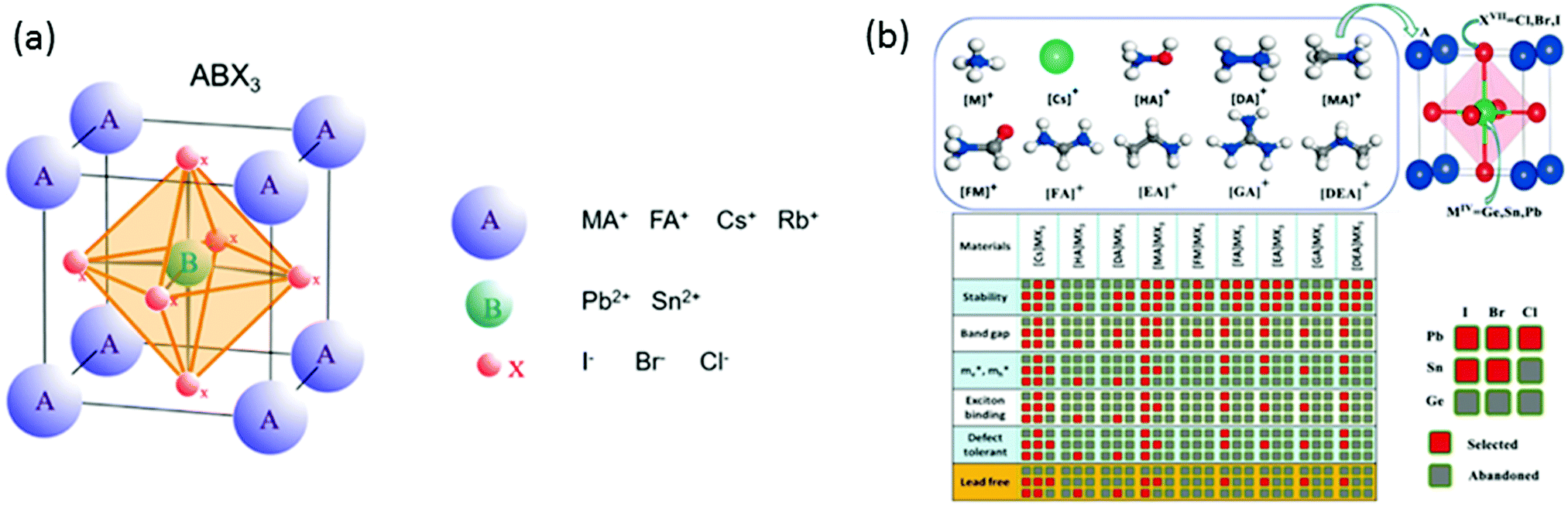 | ||
| Fig. 3 (a) Perovskite structure.35 (b) Matrix of the potential ion combinations for a library of ABX3 perovskites including: Cs+, ammonium NH4+ (M), hydroxylammonium NH3OH+ (HA), hydrazinium NH2NH3+ (DA), methylammonium CH3NH3+ (MA), formamide NH3COH+ (FM), formamidinium CH(NH2)2+ (FA), ethylammonium CH3CH2NH3+ (EA), dimethylamine NH2(CH3)2+ (DEA) and guanidine amine C(NH2)3+ (GA) for the A site; Ge, Sn and Pb group-IV metalloids (MIV) for the B site; and Cl, Br and I halogens (XVII) for the X site. Each column of the matrix corresponds to one class of the nine compounds with fixed A cation. The red and the grey squares indicate the more (selected) and the less (abandoned) promising ion combination to prepare ABX3 perovskites for solar cell application, respectively. The selection takes into account stability, band gap, effective electron–hole masses (me* mh*), exciton binding energy and defect tolerance. Lead-free combinations are highlighted in yellow in the last row36 (reprinted with permission from Chem. Mater., 2017, 29(2), 524–538. Copyright 2019, American Chemical Society). | ||
2.3 Common HTLs and trend
The anode of an inverted structure PSC (p-i-n), which is the part of thin film solar cells where the holes are collected from the active layer, consists of a Hole Transport Layer (HTL) deposited on a glass or flexible substrate. This substrate is doped, in order to be conductive, most commonly with Indium Tin Oxide (ITO); however, recent research has demonstrated ITO free substrates based on graphene, allowing for the anode to be deposited with low temperature and less costly environmentally friendly techniques, on any type of substrate and even to be freestanding.37–39 The selection of the most suitable Hole Transport Material (HTM) that will create the thin HTL film needs to be based on certain criteria. It should have high conductivity, combined with high hole mobility (ideally >10−3 cm2 V−1 s−1), as well as thermal and photochemical stability and the ability to create pinhole free, homogeneous and dense films, using solvent based techniques. Its two-fold role is to prevent the direct contact between the perovskite and conductive glass, which minimizes charge recombination and avoids short circuits, and to extract positive charges (holes) from the perovskite and transport them to the electrode. These features can have a major impact on device parameters, e.g. open circuit voltage (VOC) via quasi Fermi level splitting. Furthermore, transparency in the visible spectrum is desirable to avoid the absorption screen effect towards the active materials/absorber. In order to avoid crystallization, an amorphous phase with a glass transition temperature above 100 °C is also required. Finally, the thickness optimization of the HTM layer (namely, the HTL) is also important to minimize the increase in the series resistance, which directly correlates with the cell fill factor (FF) reduction. Usually, the optimal thickness of the HTL lies within the 20–100 nm range for the planar inverted type devices.It is the first component during the device fabrication process and the most critical one, since this is the layer on which the perovskite crystals will be grown. It has been shown that the under-layer has a major influence on the perovskite crystal orientation, grain size and morphological defects. These factors are crucial for highly efficient PSCs. Being the under-layer in the case of inverted planar PSCs, the HTL has a great effect on the crystallization process. Large perovskite grain size is generally believed to result in increased carrier diffusion length and mobility of carriers. Furthermore, a crystal structure with large grains can provide good surface coverage and a small grain boundary area, which are also desirable since they can minimize the presence of pinholes and charge traps, effectively reducing carrier recombination.40 In this context significant attention has been paid to employing the optimum hole transporting materials that yield devices with high PCE and good stability.
In particular, for the p-i-n structure devices, the first HTM that has been used is the polymer mixture of poly(3,4-ethylenedioxythiophene) polystyrene sulfonate (PEDOT:PSS). This HTM has been widely used in OPVs, the “ancestor” of inverted PSCs, for many years and the existing expertise has led to devices that exceed 17% of efficiency.41 However, this high efficiency device was achieved after doping of PEDOT:PSS with 2,3,5,6-tetrafluoro-7,7,8,8-tetracyanoquinodimethane (F4-TCNQ), a fluorinated molecular p-type dopant, while the reference, undoped device reached only 13.3%, which is the typical PCE obtained with this particular HTM. Other dopants, such as NaCl and NH4, have also managed to raise the FF to over 80% and achieve devices with extremely high VOC values (1.08 V), still with control devices of undoped PEDOT:PSS not exceeding 15% though.42 In general, pristine PEDOT:PSS suffers from very low conductivity and inhomogeneous electrical properties. Moreover, it can cause degradation of the device and reduce the device durability because of the detrimental effects of its strong acidity (pH ∼ 1) and hygroscopicity. Additionally, other drawbacks of PEDOT:PSS, compared to inorganic material layers, are the tricky control of the perovskite deposition onto a soft polymeric surface and relatively small open circuit voltage (VOC) values of PSCs.43
The record high PCE in inverted PSCs belongs to the organic polymer poly(bis(4-phenyl)(2,4,6-trimethylphenyl)amine) (PTAA), which has achieved a stabilized power output approaching 21% at the maximum power point.31 PTAA is an excellent hole-transporting and electron-blocking semiconducting material due to its electron-rich components. It has been reported that the use of PTAA can substantially improve the open-circuit voltage (VOC) and fill factor (FF), thus making PTAA the best polymer HTL yet for perovskites, typically achieving a PCE over 20%.44
Great advances have also been made in the preparation of inorganic hole transport materials. Especially nickel oxide has emerged to be highly promising, reaching efficiencies that exceed 20%, comparable to the ones with the organic HTLs.45 NiOx has a wide band gap, low absorption losses in the visible spectral range, good chemical stability, and suitable energy level alignment with the perovskite layer, which can facilitate hole collection and improve the stability of devices. However, the performance of NiOx in PSCs is still not satisfactory because of lower fill factor (FF) or short-circuit current density (JSC). One of the key reasons is the low intrinsic conductivity of NiOx, which increases the chances of charge recombination and reduces the charge collection.46,47 In order to surpass this problem and enhance the beneficial electrical characteristics of NiOx, several materials have been used as dopants, such as lithium (Li),48 rubidium (Rb),46 silver (Ag),49 lanthanum (La),50 cobalt (Co)51 and copper (Cu); the latter having also exhibited the potential of flexible devices.52 However, as in the case of most HTLs that are being used so far, the necessity of a dopant is crucial in NiOx as well, for obtaining highly efficient devices.
Apart from nickel oxide and its derivatives, other oxides have also been used and have exhibited interesting results. Vanadium pentoxide (V2O5) has been incorporated in inverted CH3NH3PbI3 PSCs and, combined with P3CT salt as the hole transport layer, has led to the realization of devices with very high FF values (0.77), which in combination with high JSC values of over 23 mA cm−2 and a VOC close to 1.1 V, achieved a final PCE close to 20%. Additionally the devices exhibited good stability, retaining more than 86% of their PCE for 30 days.53
Molybdenum trioxide (MoO3) has been widely used in organic solar cells (OPVs) as a buffer layer and as a HTL, replacing PEDOT:PSS, presenting better environmental stability, high work function, high optical transparency, and non-toxic nature. In PSCs the incorporation of MoO3 in an inverted perovskite solar cell, of the structure ITO/molybdenum trioxide (MoO3)/PEDOT:PSS/CH3NH3PbI3/fullerene (C60)/bathocuproine (BCP)/lithium fluoride (LiF)/aluminum (Al), has led to a PCE of 18.8%, with a high VOC close to 1 V and a short circuit current density of 22.6 mA cm−2.54 After elimination of the ITO, by replacing it with graphene, a TCO free device attained a PCE of 16.1%, which is highly promising for flexible devices, as well as for reducing the cost of large area devices, which arises from the TCO substrate used so far. Despite some promising results reported in the literature, the use of MoO3 in PSCs has been restricted by the demanding deposition methods, namely thermal evaporation, which is used in the highest performing devices.
Finally, some attempts at employing tungsten trioxide (WO3) as a HTL in inverted perovskite solar cells have also been reported, with the devices exhibiting a PCE of less than 10% though,55,56 even though the low toxicity is an argument in favor of WO3 (Table 2).
| HTM | Structure | μ h [ cm2 V−1 s−1] | Price per gram [€] (indicative) | PCEmax [%] | Ref. |
|---|---|---|---|---|---|
| PEDOT:PSS: poly(3,4-ethylenedioxythiophene)polystyrene sulfonate |

|
1 × 10⁻² | 166 | 17.22 | 41 |
| PTAA: poly(triarylamine) |
|
10−2–10−3 | 1145 | 21.51 | 31 |
| Spiro-OMeTAD: 2,2′,7,7′-tetrakis[N,N-di(4-methoxyphenyl)amino]-9,9′-spirobifluorene |
|
1.67 × 10⁻⁵ | 422 | 23 (normal structure) | 10 |
| NiOx: nickel(II) oxide |

|
0.14 | 14 | 20.65 | 45 |
| V2O5: vanadium pentoxide |
|
0.23 | 49 | 19.7 | 53 |
| MoO3: molybdenum trioxide |
|
0.4 | 22 | 18.8 | 54 |
| WO3: tungsten trioxide |

|
0.25 | 15.6 | 7.68 | 55 |
Among the inorganic materials that are currently at the center of research as alternative HTLs, materials based on Cu have demonstrated the most promising results so far. Cu based materials have been used in photo-electrochemical cells for many years. In fact, the simplest electrochemical cell can be made from Cu and zinc metals with solutions of their sulfates. In the process of the reaction, electrons can be transferred from the zinc to the Cu through an electrically conducting path as a useful electric current. Hence, it is not groundbreaking that these materials would be efficient as electrodes in PV cells of this type. In DSSCs, Cu derivatives have been used with great success as a redox couple in the electrolyte,57 as a dye compound,58 as counter electrodes59 and in full Cu based devices,60 which have all exhibited very promising results. It is worth noting that one of the highest efficiencies obtained in DSSCs, reaching 12%, has been with the use of a Cu redox mediator,61 while a solid state DSSC has been introduced, where Cu has been used as the HTM.62 This is one clear indication that Cu based materials have the ability of efficient charge transport. In addition, materials based on Cu have been widely used in quantum dot sensitized solar cells, mainly as counter electrodes, and recently as a dopant,63 which is an additional indication of their capability for efficient charge transport.
Their main advantage compared to other inorganic HTMs is their wide range of combinations, which result in novel materials that can be achieved with simple, low temperature and low-cost methods, giving them the potential of scale up. It is no wonder, then, that a lot of effort is made in incorporating these materials in PSCs, not only as HTLs, but also in different parts of the device, thus unraveling their limitless applications.
2.4 Challenges related to device upscaling, with a focus on stability and cost
In order to move to the upscaling of PSCs, several factors need to be taken into account, considering the manufacturing parameters that determine the PCE, the stability and the cost of the corresponding modules and panels. The fabrication techniques for each layer that PSCs are comprised of are an important parameter for the commercialization of this technology. Simple, fast, low temperature and low-cost methods are required in order to minimize energy and material losses and to maximize the potential profit. Taking into consideration that the HTL is one of the most costly layers of a PSC, it is of high importance that it can be prepared by using a variety of alternative methods. This is determined by the HTM that will be employed. The deposition methods that have been used so far for the fabrication of large area solar cells and modules are solvent based: spin coating, doctor blading, screen printing, drop casting and slot die coating are the most commonly employed techniques regarding the deposition of the HTL. Even though high PCEs have been obtained using these methods (Table 3), the amount of material that is “lost” during the deposition, combined with the high cost of organic and polymeric HTMs (e.g. spiro-OMeTAD, PTAA), increases the final price of the product.| PCE [%] | Active area [cm2] | HTM | Institute | Ref. | |
|---|---|---|---|---|---|
| 1 | 20.1 | 0.049 | Spiro-OMeTAD | University of Toronto | 64 |
| 2 | 18.1 | 0.096 | PEDOT:PSS | Kyung Hee University | 65 |
| 3 | 20.44 | 0.1 | Spiro-OMeTAD | Xi’an Jiaotong University | 66 |
| 4 | 18.55 | 0.12 | Spiro-OMeTAD | NREL | 67 |
| 5 | 17.04 | 0.125 | Spiro-OMeTAD/P3HT | CHOSE | 68 |
| 6 | 22.1 | 0.16 | PTAA | UNIST | 69 |
| 7 | 14.6 | 0.64 | Spiro-OMeTAD | EPFL | 4 |
| 8 | 20.9 | 0.991 | N 2,N2′,N7,N7′-Tetrakis(9,9-dimethyl-9H-fluoren-2-yl)-N2,N2′,N7,N7′-tetrakis(4-methoxyphenyl)-9,9′-spirobi[fluorene]-2,2′,7,7′-tetraamine | KRICT | 10 |
| 9 | 20.18 | 1 | Spiro-OMeTAD | EPFL | 70 |
| 10 | 20.3 | 1 | PTAA | Potsdam University | 32 |
| 11 | 19.7 | 1 | PTAA | UNIST | 69 |
| 12 | 18.75 | 1.02 | NiO | NIMS | 71 |
| 13 | 16.2 | 1.02 | NiMgLiO | NIMS | 72 |
| 14 | 19.5 | 1.1 | Spiro-OMeTAD | University of Toronto | 64 |
| 15 | 17.33 | 1.2 | Spiro-OMeTAD | NREL | 67 |
| 16 | 17.05 | 1.1275 | Spiro-OMeTAD | Xi’an Jiaotong University | 66 |
| 17 | 16.7 | 1.3 | PEDOT:PSS | RCNPV | 73 |
| 18 | 14 | 9.06 | PTAA | GIST | 74 |
| 19 | 18.7 | 9.1 | Spiro-OMeTAD | NREL | 75 |
| 20 | 13 | 10.1 | Spiro-OMeTAD/P3HT | CHOSE | 68 |
| 21 | 12.2 | 10.5 | N/A | Solliance | 76 |
| 22 | 14.06 | 11.09 | Spiro-OMeTAD | NREL | 67 |
| 23 | 15.4 | 11.25 | PEDOT:PSS | RCNPV | 73 |
| 24 | 10 | 16.5 | N/A | IMEC | 77 |
| 25 | 17.3 | 17.277 | N/A | Microquanta Semiconductor | 78 |
| 26 | 15.8 | 17.6 | Spiro-OMeTAD | Shanghai Jiaotong University | 79 |
| 27 | 10.46 | 31 | Carbon | NTUS | 80 |
| 28 | 12.1 | 36.1 | Spiro-OMeTAD | Shanghai Jiaotong University | 79 |
| 29 | 12.9 | 40 | PEDOT:PSS | Kyung Hee University | 65 |
| 30 | 10.4 | 49 | Carbon | Huazhong University | 81 |
| 31 | 11.2 | 50 | Spiro-OMeTAD | EPFL | 4 |
| 32 | 12.6 | 50 | Spiro-OMeTAD | CHOSE | 14 |
| 33 | 10.74 | 70 | Carbon | NTUS | 80 |
| 34 | 10.1 | 160 | N/A | Solliance | 76 |
| 35 | 6.6 | 198 | Carbon | Swansea University | 82 |
| 36 | 11.7 | 703 | N/A | TOSHIBA | 83 |
| 37 | 11.6 | 802 | N/A | TOSHIBA | 83 |
Research on metal and transition metal oxides, and other inorganic and organic materials as potential HTMs is intensive and has presented very promising results. However, it is very important to note that there is a great variation when these results move to the application from small area to large area devices. The processing methods, the stability of materials as well as the interfaces that are formed, and the cost are of prime concern. Even though the “champion devices” that have been achieved so far incorporate organic molecules, namely spiro-OMeTAD in the normal structure, and PTAA for the inverted structure, their stability problems and high cost make them far from ideal candidates for large scale application (Fig. 4).
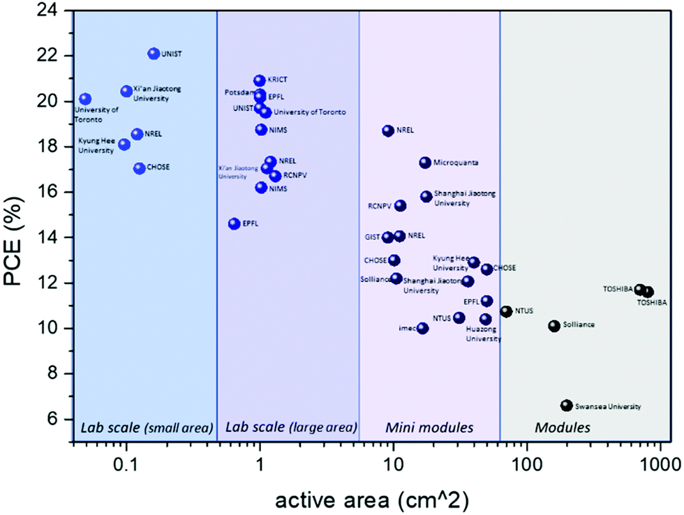 | ||
| Fig. 4 PCEs for lab-scale and large area cells and modules. | ||
PEDOT:PSS, which is widely used as the HTL in inverted PSCs, is hygroscopic, which is detrimental to the stability of the PSC. NiOx is another popular alternative to PEDOT, and it can be deposited using scalable deposition techniques such as sol–gel, spray pyrolysis, atomic layer deposition, sputtering and electrodeposition.84 However, NiOx-based HTLs are usually annealed at 300–500 °C to increase their crystallinity and conductivity, which hinders the use of NiOx-based HTLs on flexible substrates.
Other potential HTLs for PSCs with long-term stability are inorganic HTLs, such as carbon nanotubes, CuI and CuSCN, which are generally denser than their organic counterparts. In one example, CuSCN was used as the HTL in a PSC, and the device achieved a lifetime of more than 1000 h (retaining >95% of the initial PCE) under full-sun illumination at 85 °C.85 These first results indicate that there is great potential for Cu based materials for enhancing the stability of devices, bringing commercialization one step closer. Further research needs to be performed, though, for the optimization of both materials and processing techniques; however there is a lot of space for investigation. The main advantage of Cu based materials as HTLs, besides their favorable charge transport properties, is their ease of handling and their low cost. Cost analysis is an important aspect of optimizing PSM design. A competitive low cost of raw materials and processing for PSM manufacture is an important factor beyond PCE and lifetime for their potential commercial application. Cai et al. calculated the cost of materials for both mesoporous structure (Module A) and planar structure (Module B) PSMs as shown in the pie charts of Fig. 5(a) and (b), respectively.86 It is clear from these charts that the main cost of the devices comes from the transparent conductive oxide (TCO) that is being used for the deposition of electron (in n-i-p) or hole (in p-i-n) transport layers. So, indirectly, this cost is also dependent on the corresponding charge transport layer. For the inverted structure, in particular, having a material that can be deposited with simple techniques (such as coating or blading) and that does not require a high annealing temperature opens the road towards TCO free devices. By using other, low cost materials, rather than ITO, as HTL substrates the consequent device cost may be significantly decreased and even though one may miss out on the highest PCE reported for the typical ITO of FTO based devices, the PCE can still remain high enough so that the energy payback time will lie within satisfactory limits. If someone adds the typical low cost of Cu based materials themselves, as the HTL precursor, it becomes obvious that these materials are worth investigating, and are bound to achieve significant results in the near future (Fig. 5).
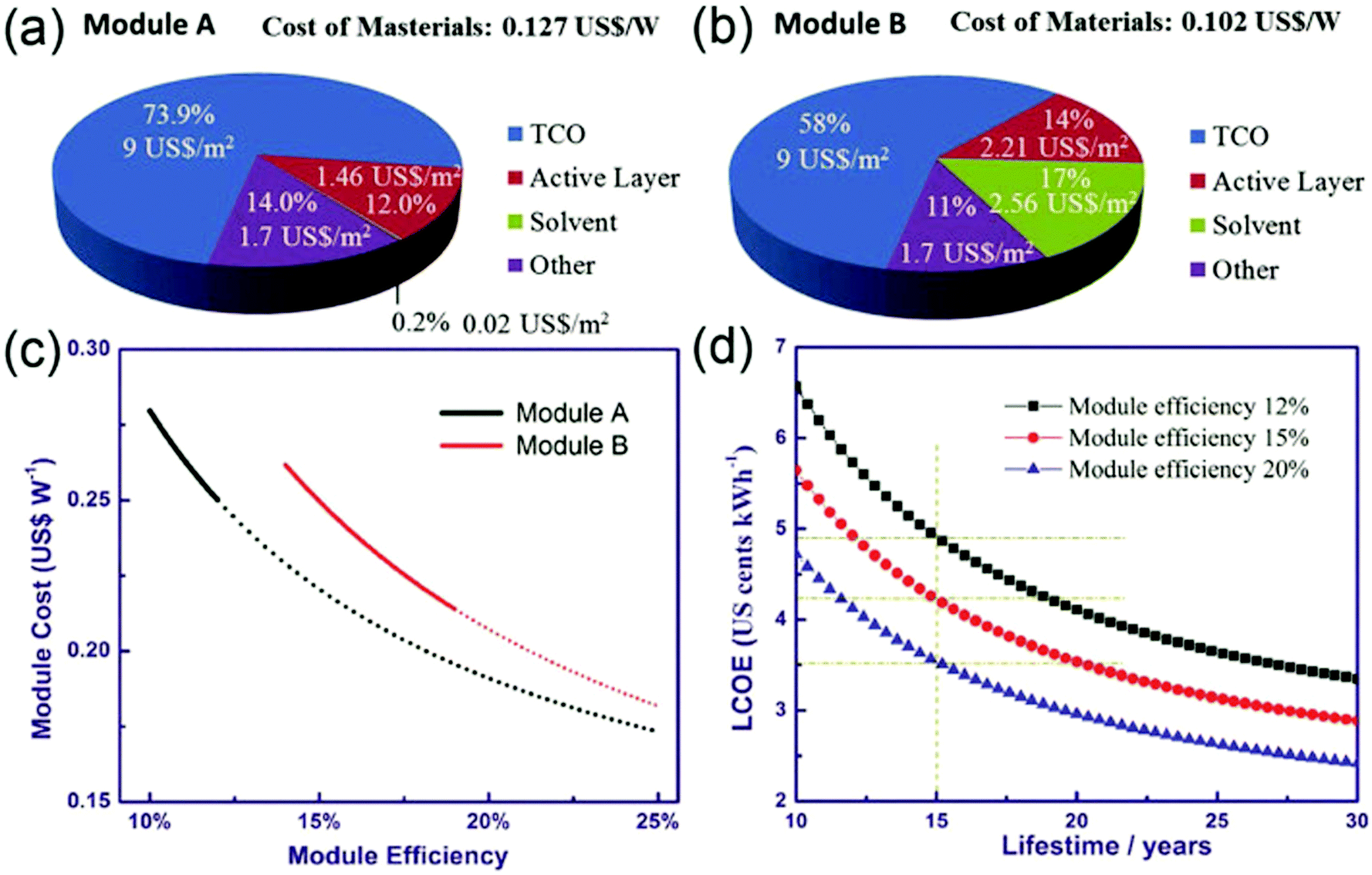 | ||
| Fig. 5 Cost distribution of materials (80% material usage ratio has been considered) for (a) Module A and (b) Module B; (c) PSM cost as a function of module efficiency; and (d) the relationship between levelized cost of electricity (LCOE) and lifetime.87 | ||
Another significant advantage of Cu based HTMs is that they can be deposited with various methods, which can be additionally performed in ambient conditions for the inverted structure, something that further facilitates the fabrication process and at the same time reduces the cost, by minimizing the equipment supply and maintenance cost.
Additionally, the elimination of dopants, which are optional in Cu based HTLs, owing to the high hole mobility of these materials, combined with the low cost of the materials themselves, renders them ideal candidates for large area applications.
With the development of materials science, more alternatives to conventional electron and hole transport layers are expected to be developed for future commercialization, among which Cu based materials seem to be of high interest and promise. In the following section by focusing on these materials, we intend to provide insight into the most recent approaches that have been reported in the literature, thus drawing the attention to novel designs of one of the most important parts of an inverted perovskite solar cell.
3. Cu based materials in p-i-n PSCs
The most significant advantage of the inverted structure PSCs is, as aforementioned, the potential for large scale application, owing to their low-temperature fabrication process, lack of hysteresis and higher stability, compared to the corresponding normal-structure mesoscopic devices. In order to further improve these assets, and at the same time reduce the cost of the resulting solar cells, significant research has been performed towards the replacement of organic HTLs that have been used so far.Inorganic HTLs being robust and humidity resistive in nature are benign for stable devices. In particular, inorganic semiconducting Cu-based HTMs, such as Cu thiocyanate (CuSCN), Cu iodide (CuI), Cu oxide (CuO) and Cu dioxide (Cu2O), have been widely used in the early third generation solar cells, while solution process techniques are widely used for depositing these materials uniformly and with good pore-filling. p-Type inorganic Cu based HTMs are economical and chemically stable. They exhibit suitable energy levels, high hole mobility, high conductivity, and excellent transmittance. Even though in the normal structure there is a great challenge for solution processing of inorganic materials on top of the perovskite, since non-suitable solvents dissolve the perovskite, this drawback is eliminated in the inverted structure devices, where the HTL is deposited prior to the perovskite. This means that this structure has great potential for exploring different materials.
From the commercialization point of view, the fabrication of solar cells using organic hole transport layers has faced a lot of obstacles, the most important of which is that they are expensive materials with stability issues. Metals such as gold and platinum are much cheaper than high purity spiro-OMeTAD and PTAA. The use of Cu based hole conductors has shown promise because they offer interesting properties, such as suitable band alignment with the perovskite active layer, high conductivity, high hole mobility and solution-processability (Table 4). Furthermore, while p-type dopants, such as Co and Li based salts, are commonly used as additives in organic HTMs to enhance the conductivity, these are hygroscopic in nature and therefore affect the overall stability of the PSCs. Cu based materials in addition to being non-hygroscopic, possess high conductivity, which makes them efficient without the addition of dopants.
| Material | Structure | E g [eV] | μ h [cm2 V−1 s−1] | Deposition method |
|---|---|---|---|---|
| CuSCN |
|
3.8 | 0.01–0.1 | 1. Spin coating |
| 2. Electrodeposition | ||||
| 3. Doctor blade | ||||
| 4. Successive ionic layer adsorption and reaction (SILAR) | ||||
| CuSeCN |
|
3.1 | 0.002 | Spin coating |
| CuI |
|
3.1 | 0.5–2 | 1. Spin coating |
| 2. Doctor blading | ||||
| 3. Chemical bath deposition (CBD) | ||||
| 4. Spray deposition | ||||
| 5. Thermal evaporation | ||||
| 6. Electrochemical | ||||
| 7. Chemical extraction | ||||
| CuS |
|
2.2 | 1–2.5 | 1. Spin coating |
| 2. Chemical bath deposition (CBD) | ||||
| 3. Successive ionic layer adsorption and reaction (SILAR) | ||||
| 4. Spray pyrolysis | ||||
| CuPc |
|
1.7 | 0.02 | 1. Vacuum deposition |
| 2. Spin coating | ||||
| 3. Glow-discharge-induced sublimation | ||||
| 4. Chemical vapor deposition (CVD) | ||||
| 5. Thermal evaporation | ||||
| CuO |

|
1.3 | 0.129 | 1. Spin coating |
| 2. Electro spray | ||||
| Cu2O |
|
2.2 | 100 | 3. Electrodeposition |
| 4. SILAR | ||||
| CuAlO2 |
|
4.5 | 3.6 | 1. Vacuum sputter |
| 2. DC sputtering | ||||
| 3. Pulsed laser deposition | ||||
| 4. RF magnetron sputtering | ||||
| 5. Chemical solution deposition | ||||
| CuCrO2 |
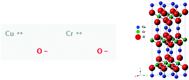
|
3.3 | 7.7 | 1. Spin coating |
| 2. Chemical solution deposition | ||||
| 3. Reactive magnetron sputtering | ||||
| 4. Spray deposition | ||||
| CuGaO2 |
|
3.6 | 0.01–10 | 1. Spin coating |
| 2. Pulsed laser deposition | ||||
| 3. Spray pyrolysis | ||||
| 4. Drop casting | ||||
Additionally, in-depth understanding of interface charge transfer and recombination is necessary for developing novel inorganic HTMs. From the perspective of optimizing the film quality of inorganic HTMs, it is of great importance to prepare high-quality homogeneous inorganic HTM films with less defects and desirable conductivity by optimizing or developing deposition techniques (vacuum deposition, spin-coating, electrodeposition, drop casting, doctor blade, pulsed laser, screen printing, spray pyrolysis and so on). A very important feature of Cu based inorganic HTMs lies in their ability to form thin films, with tunable properties, with simple, low cost, solution-based methods, as shown in Table 4. Finally, these materials are characterized by high optical transmittance, which is essential in the case of an inverted structure in order to avoid losses of incoming photons. Taking the above features into consideration, the trend of research moving to these inorganic HTLs is only rational and many groups have been focusing on replacing the organic HTLs used so far with Cu based materials as will be discussed in detail in this section.
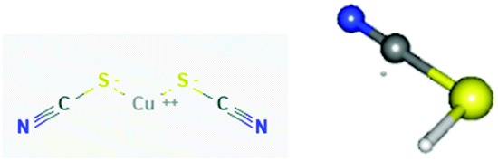
3.1 Cyanates (CuSCN and CuSeCN)
CuSCN is a molecular, metal pseudohalide of singly ionized copper, the properties of which have been studied since the first half of the twentieth century.88 CuSCN as an inorganic HTL has exhibited the most promising results, hence it has been the latest trend in PSCs. It has been initially used in organic solar cells, where the potential for increased PCE using this material has been demonstrated,89 while novel preparation strategies have further raised the efficiencies obtained. In particular, Du et al.90 have proposed an environmentally friendly way to prepare CuSCN films, from aqueous solutions, replacing in that way the commonly used organic solvent DES (diethyl sulfide), with a simple spin coating process applied under ambient conditions. The organic solar cells that have been fabricated with this method yield efficiencies of 10.7%, higher than the 9.2% achieved with the CuSCN HTL prepared in DES as a solvent and higher than the 9.7% achieved with PEDOT:PSS. Additionally, the devices exhibited enhanced stability, retaining >95% of the initial FF value for more than 600 h of constant illumination. The same procedure has been applied for HTL films that were further used in inverted structure solar cells employing the CH3NH3PbI3 perovskite. A remarkable increase in the PCE values has been noted, when changing from PEDOT:PSS to CuSCN, from 12.4% to 17.2% respectively, making this approach highly promising for application in large area devices (Fig. 6). However, to the best of our knowledge, this method has not yet been applied widely to inverted PSCs and its application in PSCs containing multiple cation perovskites, that have exhibited the highest efficiencies so far, would be highly intriguing. Additional doping of CuSCN with the fluorinated fullerene derivative C60F48 has led to a further increase of the obtained VOC values and FF of organic solar cells, which reached a final PCE of 6.4%; however this technique has not been applied to PSCs yet, but looks promising.91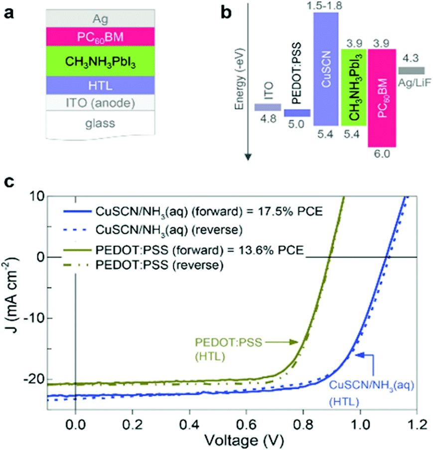 | ||
| Fig. 6 (a) Schematic cross-section of the cell architecture employed; (b) corresponding material energetics; and (c) J–V characteristics measured under simulated 1 sun solar illumination for the champion CH3NH3PbI3 solar cells based on CuSCN/NH3 (aq) and PEDOT:PSS HTLs.90 | ||
Another method that has been used to increase the PCE of CuSCN devices and has actually yielded the highest efficiencies so far, combined with excellent stability, is the addition of a conductive reduced graphene oxide spacer layer between CuSCN and the metal electrode in the normal structure devices.92
A stabilized PCE of 20.2% has been recorded with the triple cation CsFAMAPbI3−xBrx (FA = CH(NH2)2+, MA = CH3NH3+). A similar approach has been successfully applied in the inverted structure by Chowdhury et al.93 An ultrathin layer of CuSCN HTL has been introduced as an interlayer in low temperature processed r-GO based inverted planar PSCs (Fig. 7). With a matched energy level, the r-GO/CuSCN bilayer HTM successfully prevented the recombination at the interface with the MAPbI3 absorber layer. Simultaneously, the r-GO/CuSCN bilayer HTL led to faster hole extraction. The r-GO/CuSCN bilayer HTL based PSC showed a PCE of 14.28% with photovoltaic parameters of VOC = 1.031 V, JSC = 18.21 mA cm−2 and FF = 0.76. Additionally, enhanced stability has been observed for the r-GO/CuSCN bilayer HTL based PSCs retaining over 90% of the initial PCE after 100 h light soaking.
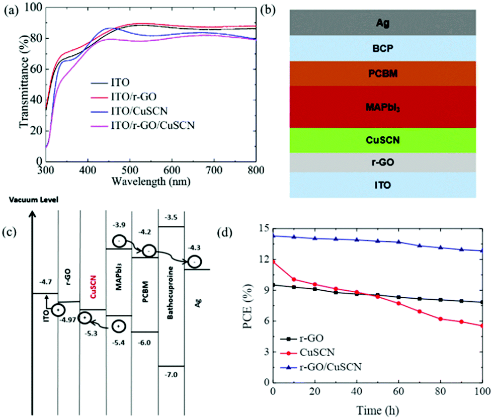 | ||
| Fig. 7 (a) Transmittance spectra of ITO, ITO/r-GO, ITO/CuSCN, ITO/r-GO/CuSCN; (b) schematic diagram of the fabricated PSC; (c) energy level diagram of the fabricated PSC; and (d) light soaking stability of the unsealed PSCs fabricated by r-GO, CuSCN and r-GO/CuSCN HTLs.93 | ||
In 2019 Park et al. have proposed the post-treatment of CuSCN films with a second –SCN containing layer, as a way to further increase the PCE of inverted PSCs.94 In their work, a solution-processed p-type CuSCN thin film was prepared for an inverted CH3NH3PbI3 perovskite solar cell. This film has been further post-treated with a solution containing a SCN− anion salt (e.g. KSCN and NaSCN). The devices showed a notable enhancement of the PCE from 11.9% to 14.9% for the post-treated films (Fig. 8). At the same time, this study revealed that the thiocyanate anion plays a critical role in improving photovoltaic performance. It was reported that excess SCN− could increase the hole conductivity of CuSCN film. In contrast, the nature of the cation of the SCN bearing salt did not have a significant effect on the device performance. The substantial improvement of JSC after post-treatment was related to improved charge collection by KSCN treatment, rather than optical modulation. The absorbance of the as-prepared films was hardly affected, which evidenced that the improved JSC was related to the improved conductivity of CuSCN and/or the better interface formed on the KSCN-treated CuSCN film.
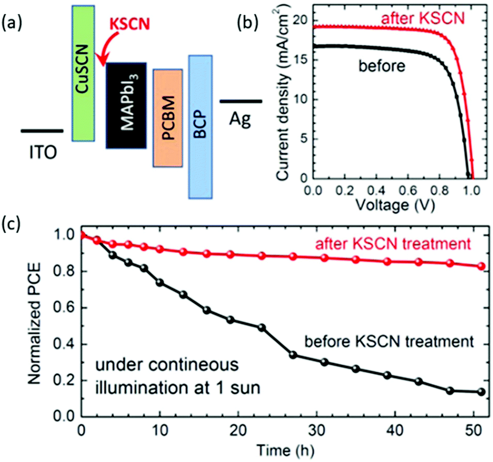 | ||
| Fig. 8 (a) The as-prepared device configuration; (b) the J–V curves of the corresponding devices with and without the KSCN post-treatment layer; and (c) time-dependent PCE of PSCs depending on post-treatment with KSCN at continuous illumination under one sun (the devices were encapsulated).94 | ||
In addition, the PCE of the devices based on untreated CuSCN degraded by 60% after 50 days in ambient humidity conditions, while 90% of the initial PCE was retained for the devices employing KSCN-treated CuSCN. The post-treated CuSCN proved to be more tolerant against humidity than the untreated one while it was also confirmed that the KSCN-treated CuSCN showed better photo-stability than the untreated. The relatively better moisture- and photo-stability was attributed to the improved interface between the perovskite and the KSCN-treated CuSCN.
An interesting approach has been recently reported by Li et al., wherein a new, facile method has been proposed to deposit high-quality CuSCN films, by using a delayed annealing treatment.95 After the CuSCN deposition, the films were left to dry at RT for 10 min and were then annealed. During the drying process, the slow evaporation of the solvent provided sufficient assembly time for the CuSCN molecules to form a dense, smooth and uniform precursor film, which then fully crystallized at 100 °C. In contrast, the direct annealing process causes the CuSCN film to form a porous structure full of voids and unavoidable structure defects and deformations due to the hasty solvent evaporation and fast crystallization processes. The PCE of the corresponding n-i-p planar device has been enhanced to 13.31%, compared to 10.32% for the direct annealed device. Moreover, by taking advantage of the superior transparency of the CuSCN films, the authors have demonstrated bifacial semitransparent n-i-p planar PSCs to avoid compromising the absorption of the perovskite absorber for the rear incidence, achieving a maximum PCE of 12.47% and 8.74% for the front and rear incidence of bifacial PSCs, respectively. This method has been reported for CuSCN deposition onto the perovskite FA0.5MA0.5PbI3−xClx (FA = CH(NH2)2+, MA = CH3NH3+) absorber, in a normal structure solar cell, while its potential in the inverted structure has not yet been explored.
The co-deposition of a hole conductor and a perovskite layer as a strategy to simplify the preparation process of PSCs has also been demonstrated and yielded promising results, when CuSCN has been added in the CH3NH3PbI3−xClx perovskite.96 A hybrid precursor solution, containing both CuSCN and CH3NH3PbI3−xClx, has been prepared and converted to a thin film, by spin coating on ITO substrates and solvent annealing. The device was completed by vacuum deposition of C60 as the electron transporter, bathocuproine as the hole blocker and Ag as the anode.
After optimizing the concentration of the CuSCN additive, a maximum PCE of 18.1% with almost no J–V hysteresis has been obtained, which is comparable to that of traditional PSCs prepared using a hole conductor and a perovskite layer by a two-step deposition process (Fig. 9). This type of PSCs with both high performance and simple preparation process are of great importance, since they have the potential of dramatically reducing the production cost of PSCs and promoting their practical application.
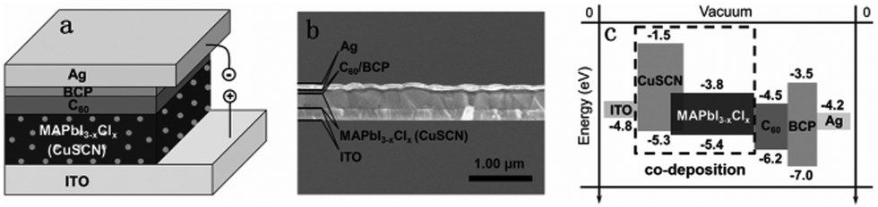 | ||
| Fig. 9 (a) The schematic illustration and (b) cross-sectional SEM image of the hybrid perovskite/CuSCN device configuration; and (c) the energy level diagram of each layer in the device.96 | ||
A new approach towards maximizing inorganic, SCN based HTL's performance has been the combination of CuSCN with other Cu+ bearing materials. Wang et al.97 demonstrated a simple but effective approach to improve the performance of inverted planar PSCs based on the CuI HTL by introducing a Cu thiocyanate (CuSCN)/CuI composite, in inverted PSCs employing the CH3NH3PbI3 perovskite. Compared to pristine CuI, the incorporation of CuSCN significantly improves the quality of the film, while maintaining high electrical conductivity, as evidenced from the results of scanning electron microscopy (SEM) and conductive atomic force microscopy (c-AFM) measurements. As a result, the champion PSCs based on the composite CuI/CuSCN HTL afforded an impressive PCE of 18.76%, which is considerably higher than the corresponding values of the respective devices using pristine CuI and CuSCN (14.53% for CuI and 16.66% for CuSCN). It is worth noting that compared with typical organic HTMs, CuSCN shows almost two orders of magnitude lower price, making it more promising for large-scale application.
Finally, very recently CuSCN has been successfully used as a dopant of the commonly used, high performance HTM poly(triarylamine) (PTAA). By adding 2% wt of CuSCN in the typically used solution of PTAA, Liu et al.98 have achieved an impressive increase in the PCE of Cs0.05FA0.81MA0.14PbI2.55Br0.45 perovskite based devices, from 14.22 to 18.16%. It was demonstrated that when CuSCN was doped into PTAA, the perovskite film showed a smoother surface morphology with a smaller RMS roughness, which might be induced by an increased perovskite grain size. The perovskite on CuSCN-doped PTAA showed a large grain size (approximately 850 nm), indicating the improved crystallization upon using the doping technique. The use of CuSCN resulted in the highest conductivity and the most p-type nature of the PTAA film, which is more suitable for charge extraction from the perovskite, while the hydrophobic property of CuSCN-doped PTAA also induced the improved perovskite quality, which further ensured a large improvement of PCE (Fig. 10).
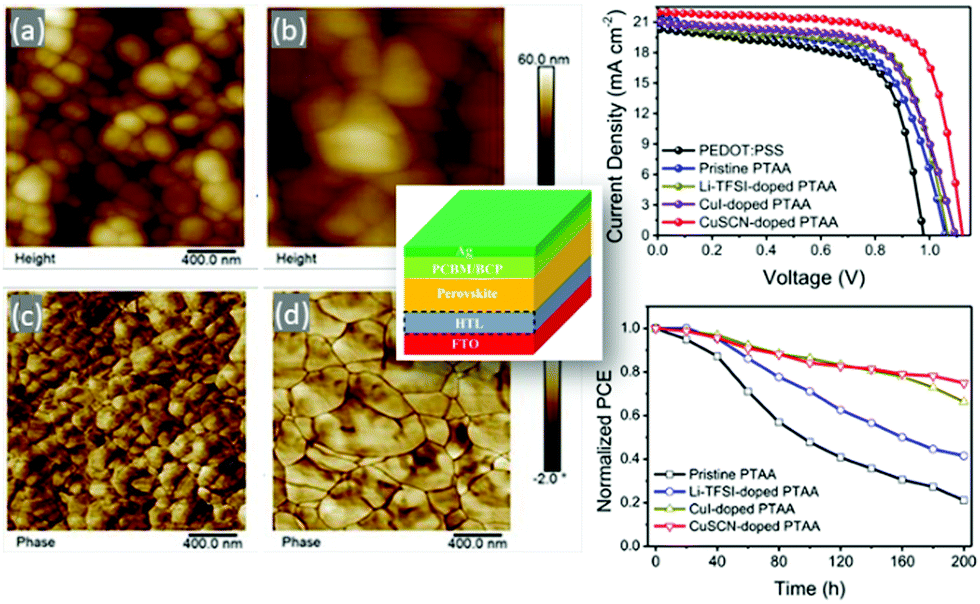 | ||
| Fig. 10 AFM height and phase images of the perovskite films on different PTAA layers: (a and c) pristine, (b and d) CuSCN-doped cases; (right) J–V curves of the PSCs based on pristine and doped PTAA as HTLs (up) and normalized PCE (down) of the PSCs based on pristine and doped PTAA for 200 h. (central image) Device architecture98 (reprinted (adapted) with permission from ACS Appl. Energy Mater., 2019, 23, 1932–1942, Copyright 2019 American Chemical Society). | ||
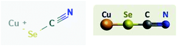
In addition to the most widely studied Cu derivatives, such as CuSCN, there has also been, to our knowledge, only one report on Cu(I) selenocyanate (CuSeCN) as an efficient hole transport material. CuSeCN is a metal pseudohalide that is structurally similar to CuSCN; however, charge transport properties and applications of CuSeCN have not been experimentally investigated. In the report of Wijeyasinghe et al.99 in 2017, the authors focused on the 3D phase of CuSeCN, which is the most stable. They synthesized the compound, by adding potassium selenocyanate (KSeCN) to a solution of Cu(I) ions, and they further proceeded to preparing a CuSeCN solution in diethyl sulfide (DES). When the CuSeCN/DES solution was spin cast on a glass substrate and annealed at 140 °C in a nitrogen atmosphere, an optically transparent layer was formed, having a typical thickness of 12–16 nm. The CuSeCN layers were incorporated in organic bulk heterojunction (BHJ) solar cells as the HTL, and the performance of these cells was compared with the cells based on the standard PEDOT:PSS HTLs. While devices based on PEDOT:PSS demonstrated a marginally better power conversion efficiency (PCE = 3.6%) with respect to cells containing CuSeCN HTLs (PCE = 3.3%), an enhancement in the open-circuit voltage (VOC) from 0.55 V (PEDOT:PSS) to 0.57 V was observed in cells containing a CuSeCN interlayer, which was primarily attributed to the deeper VBmax energy of CuSeCN (−5.1 eV) relative to the work function of PEDOT:PSS (−5.0 eV); these preliminary results revealed the potential of CuSeCN as a novel HTL material for solar cell applications. However, its application in PSCs has not yet been reported.
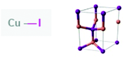
3.2 Iodides (CuI)
Apart from Cu thiocyanate, Cu iodide (CuI) has also attracted great attention due to the large bandgap, high conductivity, low cost and solution processability, and has been widely used as a HTL in organic solar cells,100,101 dye-sensitized solar cells,102 and PSCs. Copper(I) iodide (CuI) is an ionic solid that exhibits three crystalline phases, namely, α, β, and γ, of which the γ-CuI zinc blende structure (cubic), known to form at deposition temperatures below 390 °C, is the most interesting for application in optoelectronics.103Although doctor-bladed CuI has been used in conventional PSCs to replace spiro-OMeTAD, the relatively low PCE of 6.0%104 resulting from low open-circuit voltage (VOC) suggests that there is still much room for improvement in performance. In spite of their relatively low efficiency, the low-cost and decent air stability of Cu-based inorganic HTLs make them potentially feasible replacements for organic HTLs in PSCs, which represents a promising step toward further development.
One of the first reports on p-i-n PSCs, incorporating CuI as the HTL, with promising results has been the work of Tian et al.105 in 2015. In this report, a low cost, solution processed method has been used to prepare hydrophobic Cu iodide (CuI) films, that served as a HTL to replace PEDOT:PSS in inverted planar heterojunction PSCs with the structure of FTO/CuI/CH3NH3PbI3/PCBM/Al. A power conversion efficiency (PCE) of 13.58% was achieved by employing CuI as the HTL, slightly exceeding the PEDOT:PSS based device with a PCE of 13.28% under the same experimental conditions. Furthermore, CuI based devices exhibited better air stability than PEDOT:PSS based devices. A similar approach was at the same time reported by Chen et al.,106 who used a different, one-step, fast deposition-crystallization method for the CH3NH3PbI3 perovskite film, in an ITO/CuI/CH3NH3PbI3/fullerene (C60)/bathocuproine (BCP)/Ag device configuration, and managed to increase the PCE to 16.8%. Furthermore, the optimized PSCs based on the CuI HTL exhibited better air stability, retaining more than 90% of the PCE for 300 h of illumination (Fig. 11).
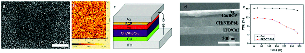 | ||
| Fig. 11 (a) SEM image of CuI film; (b) AFM image of CuI film; (c) schematic illustration of the structure of a PSC based on the CuI hole transport layer; (d) SEM cross-sectional image of the corresponding perovskite device; and (e) PCE of unencapsulated PSCs with CuI or PEDOT:PSS HTLs as a function of exposure time to ambient atmosphere106 (reproduced from ref. 106 with permission from The Royal Society of Chemistry). | ||
In order to further enhance the PCE, Wang et al.107 synthesized CuI film by exposing a thermally evaporated Cu film to iodine vapor and applied it as a HTM in inverted planar PSCs. A PCE of 14.7% was achieved along with long-term stability under ambient conditions due to the hydrophobic nature of the CuI layer. This work implies that development of novel preparation methods of CuI could hold great potential in achieving highly efficient and stable PSCs. Very recently, a different approach was proposed by Cao et al.108 In their work they prepared a hybrid nanostructure of Cu@CuI with Cu NWs embedded in CuI films, which was then employed as the HTM to fabricate inverted planar PSCs, incorporating the triple cation (CsFAMA)Pb(BrI)3 (FA = CH(NH2)2+, MA = CH3NH3+) perovskite. The outer CuI achieved efficient charge extraction, and the inner Cu then facilitated the rapid charge transfer, further resulting in an improved photovoltaic performance (Fig. 12). The best PCE for PSC devices was up to 18.4%. These devices outperformed the reference devices based on pure CuI (17.5%) and commonly used PEDOT:PSS (16.9%). Furthermore, together with the introduction of the mixture of PCBM and ZnO nanoparticles as the ETM, the best PCE of inverted planar PSC devices was remarkably improved up to 18.8%.
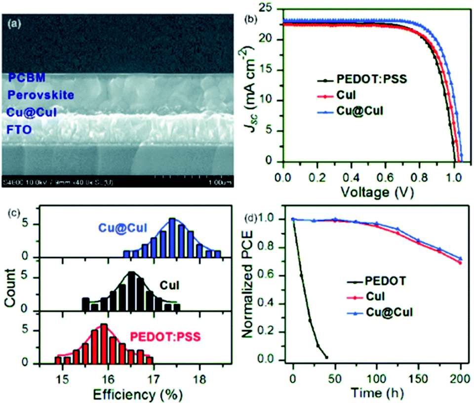 | ||
| Fig. 12 (a) Cross-sectional SEM image of an inverted PSC with Cu@CuI as the HTM and PCBM as the ETM; (b) best J–V data; (c) histograms of cell efficiencies among 30 cells of PSCs with various HTMs; and (d) stability of PSCs with PCBM as the ETM and various HTMs stored in air at RT with a humidity of about 45%.108 | ||
The long-term stability of the corresponding PSCs against humidity was further improved unprecedentedly, and the chemical reaction of the perovskite and metal electrode was avoided. Their results demonstrated that the integration of the Cu@CuI hybrid nanostructure as the HTM and the mixture of PCBM and ZnO as the ETM is a good approach to solve the PCE and stability problems in inverted PSCs.
A very promising and novel approach which has yielded the highest PCE so far in CuI based materials used as HTLs in inverted structure PSCs is that proposed by Ye et al.109 By incorporating a novel p-type conductor Cu(thiourea)I [Cu(Tu)I] in the perovskite layer, they have managed to effectively passivate the trap states of the perovskite via interactions with the under-coordinated metal cations and halide anions at the perovskite crystal surface.
In their study they have shown that the incorporated Cu(Tu)I can participate in the construction of the p-i-n bulk heterojunctions with the perovskite, leading to an increase of the depletion width from 126 to 265 nm, which is advantageous for accelerating hole transport and reducing charge carrier recombination. After optimization, the p-i-n structure PSCs that have been fabricated, with the ITO/MAPbI3−xClx/C60/BCP/Ag configuration, have reached a PCE of 20%, with an impressively high VOC, exceeding 1.1 V (Fig. 13).
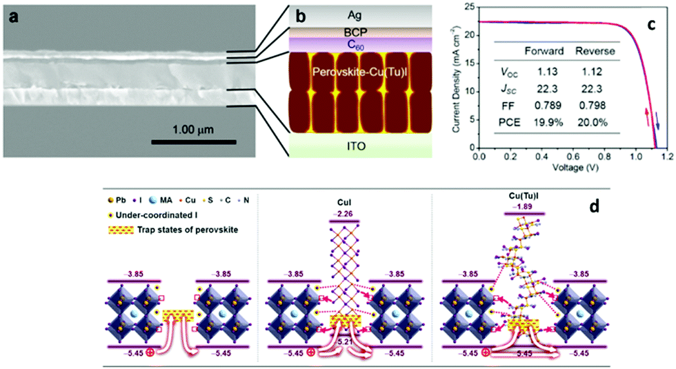 | ||
| Fig. 13 (a) Cross-sectional SEM image of the device with Cu(Tu)I as the transport layer; (b) the corresponding schematic illustration of the device architecture; (c) J–V curves of the device with Cu(Tu)I in the perovskite layer measured in the forward and reverse scan directions; and (d) schematic illustration of the possible mechanism for the trap state passivation109 (reprinted with permission from J. Am. Chem. Soc., 2017, 139(22), 7504–7512, Copyright 2017 American Chemical Society). | ||
3.3 Sulfides (CuS)
Copper sulfide is a binary inorganic material with the general formula CuxSy. It is present in both synthetic materials and minerals in the form of CuS (covellite) and Cu2S (chalcocite) and is one of the most important metal chalcogenides, attracting much interest in research due to its special properties and potential applications. Owing to its high electrocatalytic activity, CuS has been widely used as a counter electrode in high PCE solar cells, mainly quantum dot and dye sensitized solar cells, while it has also been proposed as a potential p-type absorber for thin film solar cells and as an interfacial layer for PSCs.110–113 Cu sulfide (CuxS, 1 ≤ x ≤ 2) has been found to form p-type transparent films and show beneficial electrical and optical properties. So far the Cu-deficient phase CuS and the mixed-phase CuxS have only been employed as HTMs in normal structure PSCs; however the research findings foretell that there is still potential for their implementation in the inverted structure as well.Lei et al.114 reported a high-mobility, room-temperature-deposited CuxS (x![[thin space (1/6-em)]](https://www.rsc.org/images/entities/char_2009.gif) = 1.75) polycrystalline film for use as a robust interfacial functional material for PVSCs of the normal structure. The inorganic CuxS polycrystalline film was deposited on the surface of spiro-OMeTAD to form a hybrid bilayer HTL, and this HTL was proven to perform better than the state-of-the-art HTL spiro-OMeTAD in terms of device PCE and long-term air stability. This bilayer HTL showed higher hole mobility owing to the high p-type conductivity and mobility of CuxS, while it also provided a better protection of the perovskite and improved device stability owing to the coverage of pinholes in the spiro-OMeTAD layer and the high hydrophobicity of CuxS. Benefitting from the good hole transport properties of CuxS and the barrier protection from the insertion of CuxS between the spiro layer and the Au electrode, the device with the configuration of FTO/SnO2/MAPbI3/spiro-OMeTAD/CuxS/Au produced a high PCE of 18.58% and demonstrated enhanced stability, both of which are superior to those of spiro-OMeTAD devices. Benefiting from the hydrophobic nature of CuxS, PVSCs retained over 90% of their initial efficiency, even after storage in air with approximately 40% humidity for 1000 h without encapsulation (Fig. 14).
= 1.75) polycrystalline film for use as a robust interfacial functional material for PVSCs of the normal structure. The inorganic CuxS polycrystalline film was deposited on the surface of spiro-OMeTAD to form a hybrid bilayer HTL, and this HTL was proven to perform better than the state-of-the-art HTL spiro-OMeTAD in terms of device PCE and long-term air stability. This bilayer HTL showed higher hole mobility owing to the high p-type conductivity and mobility of CuxS, while it also provided a better protection of the perovskite and improved device stability owing to the coverage of pinholes in the spiro-OMeTAD layer and the high hydrophobicity of CuxS. Benefitting from the good hole transport properties of CuxS and the barrier protection from the insertion of CuxS between the spiro layer and the Au electrode, the device with the configuration of FTO/SnO2/MAPbI3/spiro-OMeTAD/CuxS/Au produced a high PCE of 18.58% and demonstrated enhanced stability, both of which are superior to those of spiro-OMeTAD devices. Benefiting from the hydrophobic nature of CuxS, PVSCs retained over 90% of their initial efficiency, even after storage in air with approximately 40% humidity for 1000 h without encapsulation (Fig. 14).
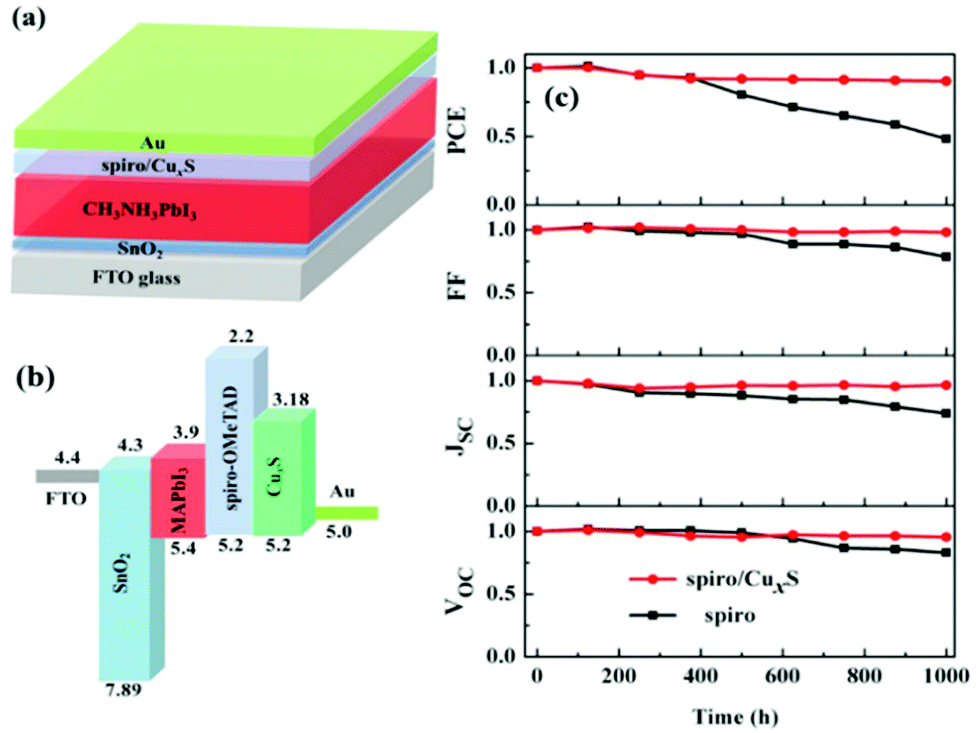 | ||
| Fig. 14 (a) Schematic illustration of the device structure of a planar n-i-p MAPbI3 solar cell, with the spiro-OMeTAD/CuxS bilayer; (b) energy band diagram of the PSC; (c) PCE, FF, JSC, and VOC as a function of ambient storage time of devices with different HTLs.114 | ||
An interesting approach has been proposed by Han et al.115 A solution-processed organic–inorganic-integrated hole transport layer which is composed of the undoped spiro-OMeTAD and Cu9S5 layer has been used in normal structure, CH3NH3PbI3 perovskite based devices, which exhibited a maximum PCE of 17.10 and 96% retention of PCE after 1200 h in an air atmosphere without any encapsulation; however this concept has not been applied in inverted structure devices.
Tirado et al.116 have proceeded to the synthesis and characterization of p-type Cu sulfide nanoparticles that have been applied as a low-cost, fully inorganic HTM in mesoscopic n-i-p PSCs. By employing CuS combined with two different perovskites, CH3NH3PbI3 (MAPbI3) and (FAPbI3)0.78(MAPbBr3)0.14(CsPbI3)0.08 (CsFAMAPbIBr), very high current densities and fill-factors were observed, suggesting an effective hole-extraction at the CuS interface, which has led to a PCE close to 14%. As a remark, the PCE values were limited by a reduced open-circuit voltage around 0.8 V, due to the phenomena occurring at the perovskite/CuS interface such as increased non-radiative recombination, caused by the considerable difference in the valence band value, and the effect of CuS metallic character. These findings contribute to fill the knowledge gap about the behavior of CuS as a HTM in PSCs due to the previously reported impossibility of having high performance CuS films on perovskites. However, this problem could be completely overcome when switching to the inverted structure, where the perovskite is deposited on the HTL and not the other way round, something that has not been performed yet, though appearing very attractive. Moreover, these results pointed out CuS as a potential extremely low-cost and stable solution-processed alternative to the state-of-the-art organic HTMs in PSCs, opening the door for new improvements and applications of this material in large-scale low-temperature produced optoelectronic devices.
An interesting approach has been adopted in 2016 by Rao et al.117 and is actually the only report so far of the CuS HTL implemented in p-i-n structure PSCs of high efficiency. By using a simple solution based process they have prepared CuS nanoparticles, which were used to modify the ITO surface and practically act as a hole extractor, in CH3NH3PbI3 PSCs of the ITO:CuS/CH3NH3PbI3/C60/BCP/Ag structure, which yielded efficiencies of 16.2%. In addition it was noted that the hysteresis effect is less conspicuous in the CuS NP-modified devices in comparison with devices based on the pristine ITO.
In a completely different context, the same group have presented semitransparent electrodes prepared with Cu sulfide thin films (CuxS) that were used for the first time in inverted-planar PSCs.118 The resulting hole-transporting-material-free and indium-tin-oxide-free (ITO-free) device showed an unprecedented 5.9% PCE. The p-type CuxS semitransparent electrode exhibited a high electrical conductivity of 1094 S cm−1, comparable to state-of-the-art transparent conductive electrodes (TCE) (Fig. 15). Surface photovoltage analysis of the grown perovskite was made, which indicated that the CuxS electrode induced an optimal band alignment in the perovskite surface while trap states were favored by using CuxS with regards to the ITO.
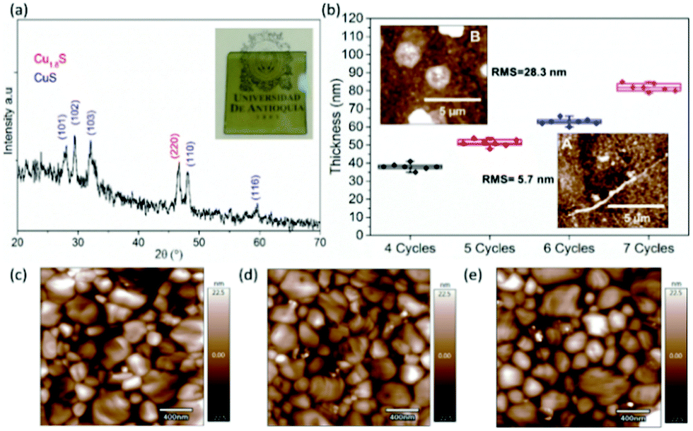 | ||
| Fig. 15 Morphology of CuxS films and the perovskite. (a) XRD pattern revealing covellite and digenite phases with the inset showing the image of a typical CuxS electrode on a glass substrate; (b) dependence of the film thickness and roughness on the deposition cycles. Inset A: AFM image of a 4 cycles film (black symbols). Inset B: AFM image of a 7 cycles film (magenta symbols). AFM topography of the perovskite surface grown on (c) ITO; (d) 4 cycles CuxS; and (e) 7 cycles CuxS.118 | ||
These results suggest that photovoltaic parameters of CuxS-based PSCs can be still improved by a better control of perovskite growth. Finally, material cost per square meter (US$ per m2) was estimated for CuxS electrodes and an impressive reduction of 77.6% was observed compared to commercial ITO. These results highlight the potential application of CuxS film as a low-cost, non-toxic and scalable p-type semitransparent electrode in PSCs and other optoelectronic devices.
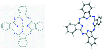
3.4 Phthalocyanines (CuPc)
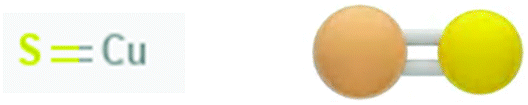
Phthalocyanine is an aromatic, intensely blue-green heterocyclic compound. Its structure is similar to that of porphine (the framework of molecules such as chlorophyll) with four fused benzene rings. It forms dye complexes with most metals in the periodic table, notably copper.Copper phthalocyanine is a brilliant blue dye with numerous applications in industrial coatings, fine art pigments, textile and paper manufacturing, and organic photovoltaic cells. It is available in both α and β forms and it is not toxic to either animals or plants. It is a typical p-type semiconductor with excellent photoelectric performance, widely employed in bulk heterojunction solar cells owing to its advantages, including high hole mobility, suitable highest occupied molecular orbital (HOMO) energy level, which matches well perovskites, long exciton diffusion length, thermal and chemical stability, low cost, and ease of synthesis. The hole mobility of CuPc (10−3 to 10−2 cm2 V−1 s−1, as compared with 4 × 10⁻⁵ cm2 V−1 s−1 for spiro-OMeTAD) is sufficient for efficient hole extraction when employing CuPc as a HTL in PSCs (>10−3 cm2 V−1 s−1), indicating a promising potential.
Even though there have been reports on normal structure PSCs employing CuPc and its derivatives, which have exhibited high PCE values reaching 18% and increased stability,119,120 the reports on the incorporation of CuPc in inverted structure PSCs that present satisfactory PCE values (>10%) are only few.
In 2018, Han et al. introduced CuPc in inverted planar PSCs, by depositing dopant-free CuPc films on ITO via a room temperature thermal evaporation process.121 Using this method they were able to obtain PSCs with high reproducibility and uniformity. The CuPc films were used as HTLs in single cation CH3NH3I3 and multication Cs0.05FA0.81MA0.14PbI2.55Br0.45 PSCs of the structure ITO/CuPc/perovskite/PCBM/BCP/Ag. An optimal CuPc film thickness of 10 nm was applied in subsequent devices and the optimized device with the single cation perovskite yielded a JSC of 18.9 mA cm−2, a VOC of 0.97 V, and a FF of 0.80, leading to a champion PCE of 14.5%, higher than the control device with PEDOT:PSS, of a maximum PCE of 13.9%. Switching to the high PCE triple cation perovskite absorber has further raised the PCE of the devices to 15.4%, while the same device configuration when transferred to flexible substrates (ITO/PEN) has yielded PSCs with a JSC of 18.5 mA cm−2, a VOC of 0.99 V, and a FF of 70%, with a maximum PCE of 12.8% (Fig. 16). The small drop in PCE observed with flexible devices, when compared with the rigid ones, is related to the higher series resistance of the flexible device;103 however, the flexible devices have exhibited excellent bending stability retaining ∼85% of the original PCE after 3000 bending cycles at r = 5 mm. Additionally, the PSCs with CuPc as the HTL exhibited better stability than PEDOT:PSS based devices when exposed to ambient air (temperature: 20–25 °C, humidity: 40–50%) without encapsulation.
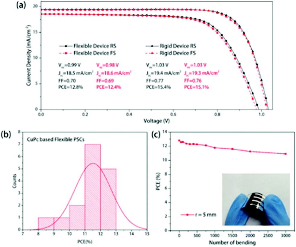 | ||
| Fig. 16 (a) J–V curves of the best-performing flexible and rigid PSC based on CuPc HTLs. The inset table shows the main parameters of the device; (b) the PCE distribution of CuPc based flexible PSCs; and (c) PCEs of flexible PSCs based on CuPc HTLs for bending cycles. The inset figure is the photograph of the corresponding flexible solar cell.121 | ||
By employing C60 as the ETL, replacing PCBM, the same group have further improved the PCE of CuPc HTL based PSCs to 16.72%, in a device employing the triple cation Cs0.05FA0.81MA0.14PbI2.55Br0.45 perovskite,122 owing to a salient increase in JSC and VOC. This has been ascribed to the higher conductivity and electron mobility of C60 compared to PCBM, contributing to a faster electron transport and suppressed recombination loss. It should be noted at this point that the well-known practice of solvent annealing has been applied to these devices, during the perovskite annealing, which has been proven to deliver uniform films of high quality, with increased crystallinity, fewer low-dimensional defects and larger grain size combined with less scattering of grain boundaries and a negligible PbI2 residual. Additionally, the devices present negligible hysteresis, as also confirmed by the low value of the hysteresis index (HI) that has been calculated. The corresponding flexible devices achieved a PCE of 12.96%, which is a very promising result for flexible PSCs. Both the C60-based and PCBM-based flexible devices maintain 81.3% and 79.6% of their initial PCE after 3000 bending cycles with a bending radius of 5 mm, exhibiting excellent stability, something that clearly indicates the suitability of CuPc as an efficient hole extraction layer in highly efficient and stable flexible PSCs (Fig. 17).
 | ||
| Fig. 17 (a) The J–V curves of the best-performing flexible PSCs based on C60 and PCBM ETLs, measured under both the reverse and forward scan direction; (b) image of the as-prepared flexible PSC; histograms of the PCE for 20 cells with (c) C60 and (d) PCBM ETLs and (e) normalized PCE of the flexible PSC as a function of bending cycles with a radius of 5 mm.122 | ||
The CuPc derivative Cu phthalocyanine-3,4′,4′′,4′′′-tetra-sulfonated acid tetra sodium salt (TS-CuPc) possesses good solubility in polar solvents, which allows its application as a HTL in low-cost PSCs. By using an aqueous solution process Wang et al.123 have prepared composite films of Cu phthalocyanine-3,4′,4′′,4′′′-tetra-sulfonated acid tetra sodium salt (TS-CuPc), doped with tetrafluoro tetracyanoquinodimethane (F4-TCNQ) with improved film conductivity and hole mobility. These films have been then incorporated in inverted structure CH3NH3PbI3 PSCs that yielded efficiencies of 16.14%, with a simultaneous increase of both current density and open circuit voltage, compared to the reference PEDOT:PSS device that reached 12.88% PCE in the same system. The TS-CuPc:F4-TCNQ-based device additionally exhibited better stability compared to the PEDOT:PSS-based one. After 350 h storage in air at room temperature, the TS-CuPc:F4-TCNQ (2.5 wt%)-based device maintained 88% of the initial PCE. In contrast, the PCE of the PEDOT:PSS-based device was rapidly reduced by half (Fig. 18). This obvious improvement of the device stability has been ascribed to the stable TS-CuPc:F4-TCNQ, with almost neutral precursor solution. However, it is worth noting that the undoped TS-CuPc did not perform well enough, yielding PCE values lower than 8%, something that constitutes a drawback regarding the cost of the corresponding devices.
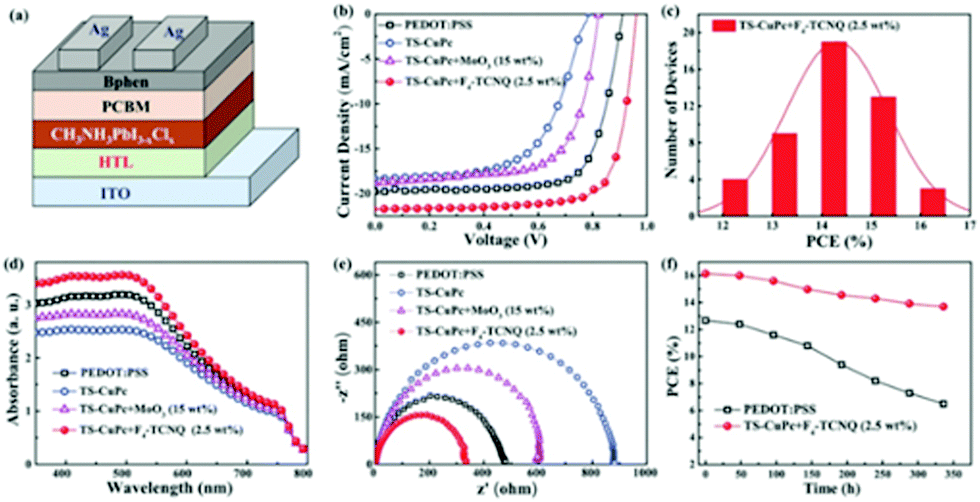 | ||
| Fig. 18 (a) Schematic diagram of the device structure in inverted PSCs incorporating different HTMs; (b) J–V curves of the PSCs using PEDOT:PSS, TS-CuPc, TS-CuPc:MoO3 (15 wt%) and TS-CuPc:F4-TCNQ (2.5 wt%) as the HTMs measured under simulated AM 1.5 sunlight of 100 mW cm−2; (c) histogram of PCEs measured from 50 TS-CuPc:F4-TCNQ (2.5 wt%)-based inverted PSCs; (d) UV-vis absorption spectra of CH3NH3PbI3−xClx perovskite films deposited on different HTMs; (e) Nyquist plots of CH3NH3PbI3−xClx-based PSCs measured in the dark, at an applied voltage of 0.96 V; (f) PCEs as a function of time in the PEDOT:PSS and TS-CuPc:F4-TCNQ (2.5 wt%)-based PSCs without encapsulation under identical storage conditions (in atmosphere, at RT).123 | ||
However, the presence of transition metals in the structure of organometallic HTMs, like CuPc, is a critical issue because these elements can lead to toxicity and carcinogenicity, which potentially cause health problems. In addition, the poor solubility of unmodified CuPc in the most common organic solvents restricts its application in solution-processable PSCs.
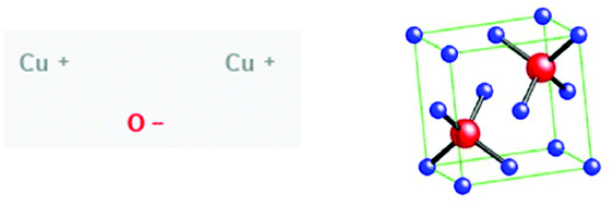
3.5 Oxides (CuO, Cu2O and CuOx)
Copper oxide is a compound from the elements of copper and oxygen and may refer to copper(I) oxide (cuprous oxide, Cu2O), copper(II) oxide (cupric oxide, CuO), copper peroxide (CuO2) or copper(III) oxide (Cu2O3). Due to the natural abundance of Cu, CuOx has become a promising alternative to PSC components. Stable Cu oxides (CuOx), namely, cupric oxide (CuO) and cuprous oxide (Cu2O), are well-known p-type semiconductors. Cupric oxide (CuO) has a band gap of 1.21–2.1 eV and a monoclinic crystal structure, while cuprous oxide (Cu2O) has a band gap of 2.2–2.9 eV and a cubic crystal structure. With their valence band maximum in good alignment with that of the most commonly used high PCE perovskites, a good photovoltage is expected from this type of HTMs when they are used as HTLs in PSCs. The first attempt to use these materials for PV application was in the late ‘70s and since then various techniques have been used to fabricate Schottky junction, hetero-junction, and homo-junction devices using them as light harvesters.124–126 However, low device performance was observed due to low absorption in the long wavelength region because of the high energy gap. Owing to their low electron affinity and high hole mobility, Cu oxides have been suggested as a potential hole transport material in heterojunction based solar cells. CuOx-based solar cells have mainly been studied by creating p–n junction device structures. The use of Cu2O has been reported in an Al–Ga–O thin-film solar cell with a maximum PCE of 6%, which is achieved using the Alx–Ga1−x–O/Cu2O heterojunction. Achieving high PCEs using these materials is still under investigation, though, because of the difficulty involved in identifying a suitable n-type semiconductor as well as concerns with the chemical instability of the CuOx surface.127A solvothermal synthetic route has been applied by Savva et al.128 to prepare cupric oxide (CuO) NPs that were synthesized from the thermal decomposition of CuCl in DMSO at low temperature (80–120 °C) and within a short reaction time (30 minutes). Dispersions of CuO NPs were used to fabricate interfacial layers of CuO without any post deposition annealing or solvent washing step. The CuO substrates exhibited a high work function, transparency and good surface properties, such as increased hydrophobicity, thus facilitating the growth of high quality perovskite layers, with increased grain size compared to PEDOT:PSS. By using CuO NPs as interfacial layers between ITO and CH3NH3PbI3, a PCE of 15.3% was obtained in a CuO-NPs/CH3NH3PbI3/PC70BM/AZO/Al configuration device. High VOC values of 1.09 V and more than 50% increase in PCE compared to PEDOT:PSS-based p-i-n perovskite-based solar cells were obtained, indicating that the nanoparticulate nature of the CuO interfacial layer leads to light management benefits for the device performance of the p-i-n PSCs. In addition, the photovoltaic performance of the CuO-based PSC is stable for more than 30 minutes under continuous 1 sun illumination, indicating no photo-chemical interaction between CuO HTL and CH3NH3PbI3. This work highlights the potential for the incorporation of CuO as a HTL in large area PSCs.
A different approach has recently been proposed by Sun et al.,129 wherein electrospun CuO nanowires are used as a buffer layer in ITO/CuO NWs/PEDOT:PSS/CH3NH3PbI3/PCBM/Bphen/Ag inverted PSCs (Fig. 19). When CuO NWs were added to the flat and pinhole-free reference film, the surface of the perovskite retained a smooth and dense morphology. Moreover, some large crystal grains with an average grain size of 770 nm could be found, indicating that the introduction of NWs does not alter the crystallinity of the perovskite layer. The introduction of CuO NWs led to a negligible decrease in light transmission relative to the ITO/PEDOT:PSS reference film, indicating that the light absorption of CuO NWs had no influence on the performance of PSCs.
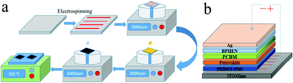 | ||
| Fig. 19 (a) Schematic illustration of the main fabrication procedure of CuO nanowires. (b) Schematic device structure of the proposed PSC129 (reprinted with permission from ACS Appl. Mater. Interfaces, 2018, 10(13), 11289–11296, Copyright 2018 American Chemical Society). | ||
The dark current of the CuO NW device was lower than that of the reference device in the low voltage/current regime, indicating a higher interface-dependent shunt resistance (Rsh) and hence an improvement in charge extraction efficiency. Overall, under one sun simulated illumination, the reference device yielded an average open circuit voltage (VOC) of 0.97 V, an average short circuit current density (JSC) of 18.33 mA cm−2, an average fill factor (FF) of 0.76, and an average PCE of 13.50%. The general trend when CuO is used as a hole transport layer instead of PEDOT:PSS is for the VOC to change, since the valence band of CuO is lower than the HOMO of PEDOT:PSS. However, in the case of CuO NWs, VOC was kept nearly constant, implying that CuO NWs do not change the electrode work function. With the increase of CuO NW coverage, the average JSC increased to 21.72 mA cm−2, while the PCE obtained with the optimal coverage of 4.2% had an average value of 16.35%, which is an enhancement of over 21% compared with that of the reference device of 13.5%. Moreover, it was found from EIS measurements that the corresponding device had the lowest series resistance (Rs) and the highest recombination resistance (Rrec) (Fig. 20).
 | ||
| Fig. 20 (a) J–V curves of PSCs with different coverage of CuO NWs, under 100 mW cm−2 illumination (AM 1.5G) and Nyquist plots of PSCs without and with the optimal coverage of CuO-NWs in the dark and (b) schematic illustration of hole transport with CuO NWs.129 | ||
These results demonstrated the feasibility of using CuO NWs as a buffer layer for improving the PCE of PSCs.
Even though there have been several reports, from 2015 and on, of planar inverted PSCs using Cu2O as the HTM, reports on efficiencies that exceeded 10% have only been few. Zuo et al. used the method of in situ conversion of CuI film in aqueous NaOH solution, to prepare Cu2O films that were later on used as the HTL for inverted PSCs of the ITO/HTM/CH3NH3PbI3/PC61BM/Ca/Al structure. The devices exhibited efficiencies of 13.35%, with a distinctively enhanced open circuit voltage (1.07 V) compared to the equivalent PEDOT:PSS based devices, which yielded a VOC of 0.95 V and a final PCE of 11.04%.130 In the same work, CuO films were also prepared by simply heating Cu2O films in air (Fig. 21). The corresponding devices with CuO as the HTL exhibited efficiencies of 12.16%, again achieving a high VOC value of 1.06 V, but hindered by lower FF and JSC values, compared to the higher performing Cu2O based devices. The significance of this work lies in the facile and low temperature method used for the preparation of films, which has the potential of applicability in solar modules of large area.
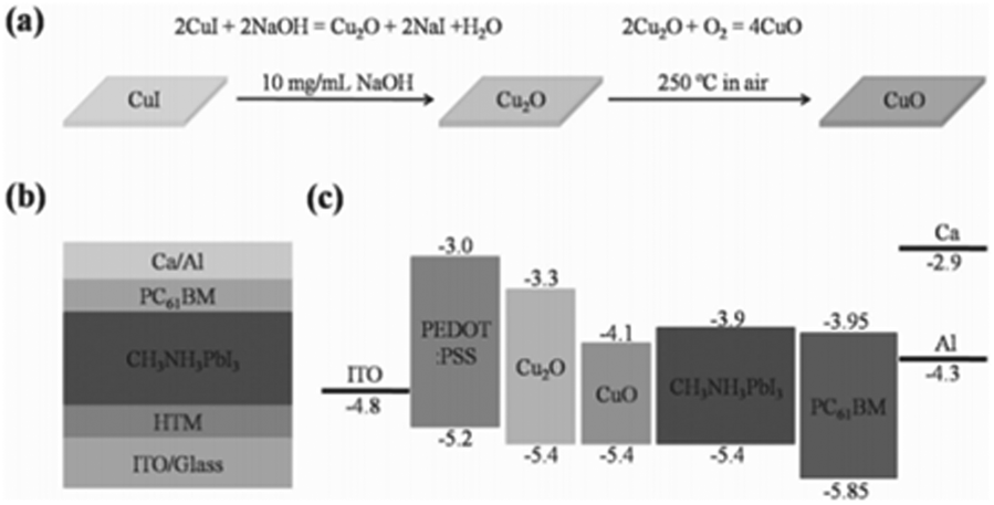 | ||
| Fig. 21 (a) Preparation process of Cu2O and CuO films; (b) device structure; and (c) energy level diagram.130 | ||
A variety of deposition methods have been proposed for Cu2O based, inverted structure devices, such as the successive ionic layer adsorption and reaction131 (SILAR) and the electrodeposition132 methods; however the resulting PSCs’ efficiencies were not very promising (8.23% and 9.64% respectively). The SILAR method resulted in low JSC values that were attributed to the large thickness of the Cu2O film,133 which increases the device's series resistance and optical losses from the light absorption of Cu2O in the partial visible region, while the poor surface morphology was responsible for the low VOC obtained. On the other hand, the low VOC and FF of the electrodeposited devices were attributed to the higher energy level offset at the ITO/CH3NH3PbI3 interface, which leads to a low charge collection PCE and a high electron–hole recombination probability, and thus restricts the photovoltaic performance.
CuOx on the other hand have provided very promising results since the report of a CuOx hole transport layer, prepared from a solution-processed method, that was introduced into inverted planar CH3NH3PbI3 PSCs, which exhibited efficiencies of >17%, by Sun et al.134 Further incorporation of ZnO as the electron transport layer (Fig. 22), replacing BCP and C60, has led to an increase in the PCE of CuOx CH3NH3PbI3 PSCs, which reached 17.43%.135
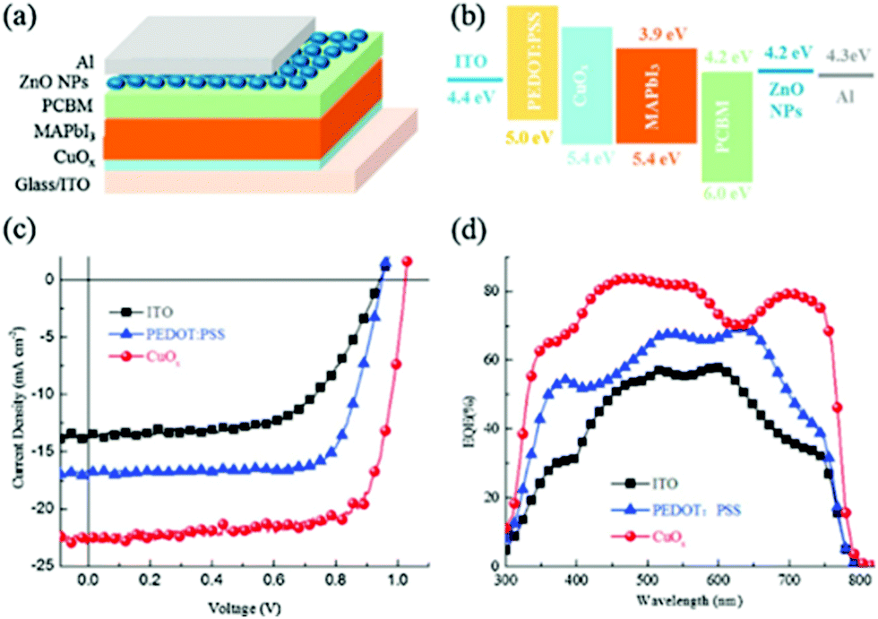 | ||
| Fig. 22 (a) Schematic of the CuOx/ZnO based device structure; (b) energy-level diagram of the corresponding device; (c) J–V curves and (d) EQE spectra of the PVSCs without or with different HTLs.135 | ||
By switching to a mixed halide perovskite, MAPbI3−xClx, an impressive PCE of 19% was achieved by Rao et al.136 The perovskite that was used in that work is MAPbI3−xClx, with various Cl doping proportions, while a PCBM (phenyl-C61-butyric acid methyl ester)/C60 double fullerene layer was deposited as an electron acceptor and collection layer. Finally, a thin film of bathocuproine (BCP) and a silver layer were thermally evaporated as the hole blocker and anode, respectively. The less intrinsic defects in the MAPbI3−xClx film, compared to MAPbI3, are greatly beneficial for reducing the recombination of charge carriers in the device. Furthermore, studies on the hole and electron mobility of the MAPbI3 and MAPbI3−xClx films revealed that the hole mobility of the MAPbI3−xClx film is much higher than that of the MAPbI3 film and the difference of electron mobility for the films is negligible. Taken together the results of the remarkable morphology and hole mobility improvement of the MAPbI3−xClx film, conspicuous intrinsic defects reduction in the film and the prominent increase of the device recombination resistance, the MAPbI3−xClx based device possesses higher VOC, FF and JSC, thus leading to an outperforming PCE. This is a significant result, which reveals the potential of further improvement of the CuOx device performance when perovskites with mixed anions and mixed cations are employed, something that has not been investigated so far, to the best of our knowledge.
Ternary, Cu based, metal oxides, such as CuAlO2, CuCrO2 and CuGaO2, have also been used as HSCs in PSCs. CuAlO2, CuCrO2 and CuGaO2 known to have a delafossite structure with the general formula of ABO2, where a sheet of linearly coordinated A cations are stacked between edge-shared octahedral BO6 layers, have been investigated in DSSCs and organic photovoltaics as p-type semiconductors. These materials, contrary to Cu2O and CuO, possess a large bandgap of over 3.5 eV with a modest hole mobility in the range of 0.1 to 10 cm2 V−1 s−1, have a high transmission in the broad wavelength range and have been tested in both regular and inverted PSCs. This type of metal oxides are generally synthesized using the hydrothermal method and then spin-coated on top of the conductive substrate in p-i-n structured PSCs.
An impressive increase in the PCE of inverted PSCs has been achieved when films of CuGaO2 nanoparticles, prepared by a surfactant-assisted hydrothermal synthesis, have been used as the HTL, replacing PEDOT:PSS. With an impressive VOC of 1.09 V for the CH3NH3PbI3 perovskite and a short circuit current density of 19.52 mA cm−2, the devices employing CuGaO2 achieved a PCE of 15.3%, while the PCE of the equivalent PEDOT:PSS devices did not surpass 9.3%137 (Fig. 23).
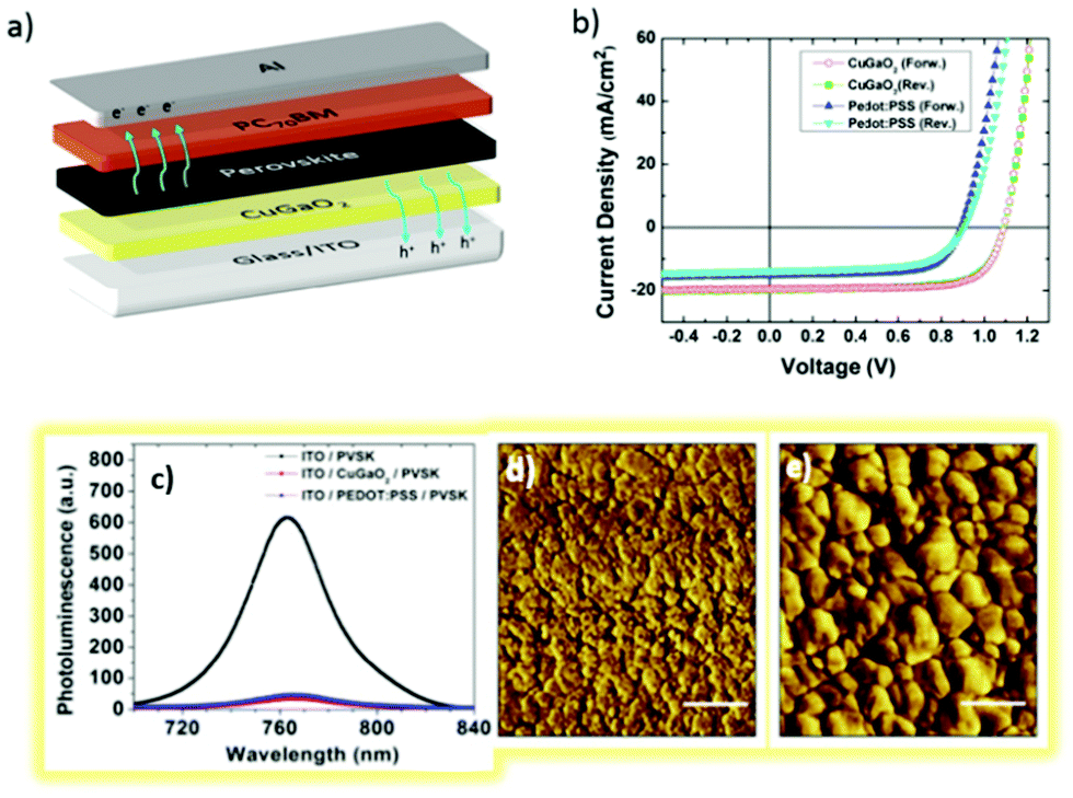 | ||
| Fig. 23 (a) The structure of p-i-n PSCs (ITO/CuGaO2-NPs/CH3NH3PbI3/PC70BM/Al); (b) J–V curves under 1 sun illumination; (c) photoluminescence spectra of CH3NH3PbI3 on top of ITO, ITO/CuGaO2-NPs, and ITO/PEDOT:PSS electrodes; (d) AFM images of ITO/CuGaO2 and (e) ITO/CuGaO2/CH3NH3PbI3 films (scale bar = 500 nm).137 | ||
When incorporated, in combination with NiOx, as a bilayer inorganic hole transport film in inverted planar and mesoporous structure PSCs, CuGaO2 has achieved a stabilized PCE of 20%, which is one of the highest reported for inverted PSCs with inorganic HTMs. Additionally, the unencapsulated PSC device retains more than 80% of its original PCE when subjected to thermal aging at 85 °C for 1000 h in a nitrogen atmosphere, thus demonstrating the superior thermal stability of the device.138 In this very interesting approach, an inverted PSC with mesoporous HTMs has been designed, in which an ultrathin NiOx (<10 nm) was introduced as the compact layer and mesoporous CuGaO2 was then deposited on it to form a bilayered, graded band alignment inorganic HTM (Fig. 24). The graded energy alignment of the VBM between NiOx, CuGaO2, and perovskite resulted to be very favorable for charge carrier transfer and collection. In this work the potential of metal oxide layers as HTLs for stable PSCs is highlighted: the CsFAPbIBr double cation perovskite is a thermally stable perovskite system in comparison with the methylammonium (MA)-containing perovskites, while the inorganic NiOx/mesoporous CuGaO2 is even more thermally stable than the (FA, Cs) double cation perovskite, which enabled the devices to retain more than 90% of their initial PCE after being stored for two months under ambient conditions. An additional doping with Zn has led to a remarkable PCE of 20.67%,139 in a methylammonium-free device, which retained over 85% of its initial PCE after thermal annealing at 85 °C for 1000 h in a nitrogen atmosphere, demonstrating the superior thermal stability of the present PSCs with the metal doped inorganic HTM.
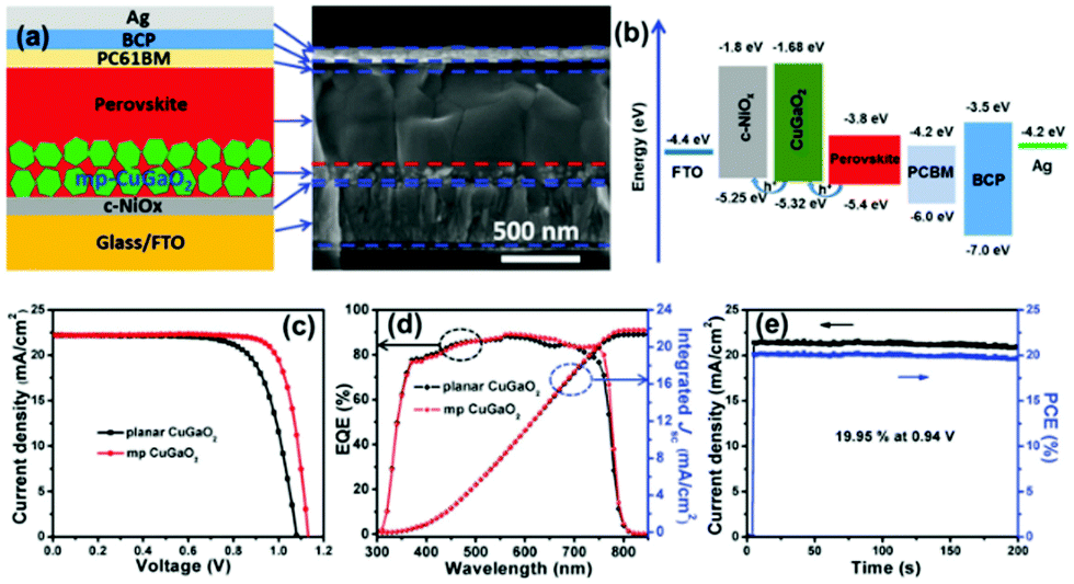 | ||
| Fig. 24 (a) Schematic illustration of the mesoporous CuGaO2 device configuration and a typical cross-sectional SEM image; (b) energy-level diagram demonstrating the collection process of photo-induced holes; (c) J–V curves of the devices based on the planar and mp CuGaO2 HTM; (d) IPCE curves and the corresponding integrated photocurrent for devices based on the planar and mp CuGaO2 HTM; (e) the steady output PCE of the champion device based on the mp CuGaO2 HTM around the maximum output power point as a function of time under simulated 1 sun illumination.139 | ||
To make a reference to another one of the highest performing examples, a composite oxide of CuGaO2 has been employed by Zhang et al.140 as the HTL in normal structure, mesoscopic PSCs of the FTO/c-TiO2/CH3NH3PbI3−xClx/CuGaO2/Au structure. In their work, CuGaO2 nanoplates have been synthesized hydrothermally and then dense films prepared, with an optimum thickness of 345 nm, which presented flat morphology with a root mean square roughness value of only 21.32 nm, by a solution process method. The best performing device achieved a JSC of 21.66 mA cm−2, a VOC of 1.11 V, and a FF of 0.77, leading to an overall PCE of 18.51% under the standard AM1.5 solar illumination, higher than the 17.14% obtained from the control spiro-OMeTAD device. The higher VOC has been attributed to better energy alignment at the CuGaO2/perovskite interface, which minimizes the charge-extraction barrier and enhances the built-in potential across the device. In addition, the enhanced JOC and FF have been interpreted as the consequences of efficient hole extraction and electron blocking of the CuGaO2 layer. Most importantly, the CuGaO2 HTL imparts not only better photovoltaic performance, but also greatly retards the decomposition of the perovskites. The PCE of the CuGaO2-based device maintained the majority of the original device performance up to 30 d, whereas that of the organic HTL (spiro-OMeTAD)-based device decayed dramatically from ≈17% to 3% within the first week. Interestingly, these results have not yet been explored in the inverted structure devices, most probably because of the relatively high thickness of the CuGaO2 film that is required; however it would be interesting to evaluate the performance of this composite in the p-i-n structure as well, together with the combination with the multication mixed halide perovskites that are currently exhibiting the highest efficiencies in both structures (n-i-p and p-i-n).
On the other hand, it has been demonstrated that a a:CuAlO2 hole selective buffer layer between the ITO electrode and PEDOT:PSS, in p-i-n structure CH3NH3PbI3 perovskite based devices, can increase the PCE of PEDOT:PSS devices from 11.1% to 14.52%, while at the same time increasing their stability.141 The PCE improvement stems from the enhanced charge extraction and reduced charge recombination due to the incorporation of a:CuAlO2 with increased conductivity and suitable work functions. The origin of this improved device performance can be traced to the increased conductivity of the added a:CuAlO2 layer and its formation of adequate energy level alignments with the PEDOT:PSS layer (Fig. 25). The pristine a:CuAlO2-based solar cell also showed markedly improved ambient stability as compared to the pristine PEDOT:PSS and a:CuAlO2/PEDOT:PSS-based devices. The pristine a:CuAlO2-based device retained more than 90% of the initial PCE even after 240 h of storage in air. In addition, the a:CuAlO2/PEDOT:PSS-based device retained 80% of its initial value while the PCE of the pristine PEDOT:PSS-based device degraded to less than 35% of its initial value. This lower stability has been implied to originate from the acidic characteristics of PEDOT:PSS that erode the ITO electrode.
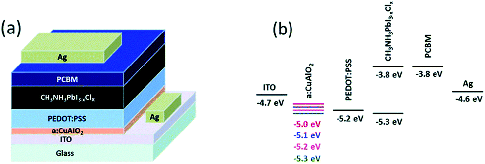 | ||
| Fig. 25 (a) Structure of a PSC with the a:CuAlO2 buffer layer and (b) energy level diagram of the device components along with various thicknesses of a:CuAlO2: red line (5 nm), blue line (10 nm), pink line (15 nm) and olive line (20 nm)141 (reproduced from ref. 141 with permission from The Royal Society of Chemistry). | ||
Recently, a composite, transparent CuAlO2/Cu–O hole transport film has been prepared by flame spray pyrolysis and incorporated in an ITO/[CuAlO2/Cu–O]/CH3NH3PbI3/PC70BM/AZO configuration inverted perovskite solar cell, which achieved a PCE of up to 16.3% with a negligible hysteresis effect.142 However, even though this value is one of the highest in a novel composite material, the high temperature that is required for the preparation of the oxide films is a limiting factor when it comes to the large area application of this process. An interesting work has been presented by Qin et al.,143 where they introduced a novel Cu-chromium binary metal oxide as the hole-transporting material for application in inverted structure PSCs. Delafossite CuCrO2 has a direct band gap of ∼3.1 eV, much larger than that of Cu oxides. Owing to its high conductivity and non-toxicity, it is a promising p-type conductive material for optoelectronic applications. By using a low temperature, sol–gel method, the authors prepared Cu acetylacetonate and chromium acetylacetonate solutions that were mixed with different volume ratios. Following, they prepared CuyCrzO2 films on ITO and PEN substrates by the simple spin coating method, on top of which the perovskite layers were grown. By varying the volume ratio of chromium acetylacetonate in the mixed solution, they were able to tune the Eg from 2.8 to 3.62 eV demonstrating that the corresponding CuyCrzO2 films are promising candidates for HTLs in PSCs (Fig. 26).
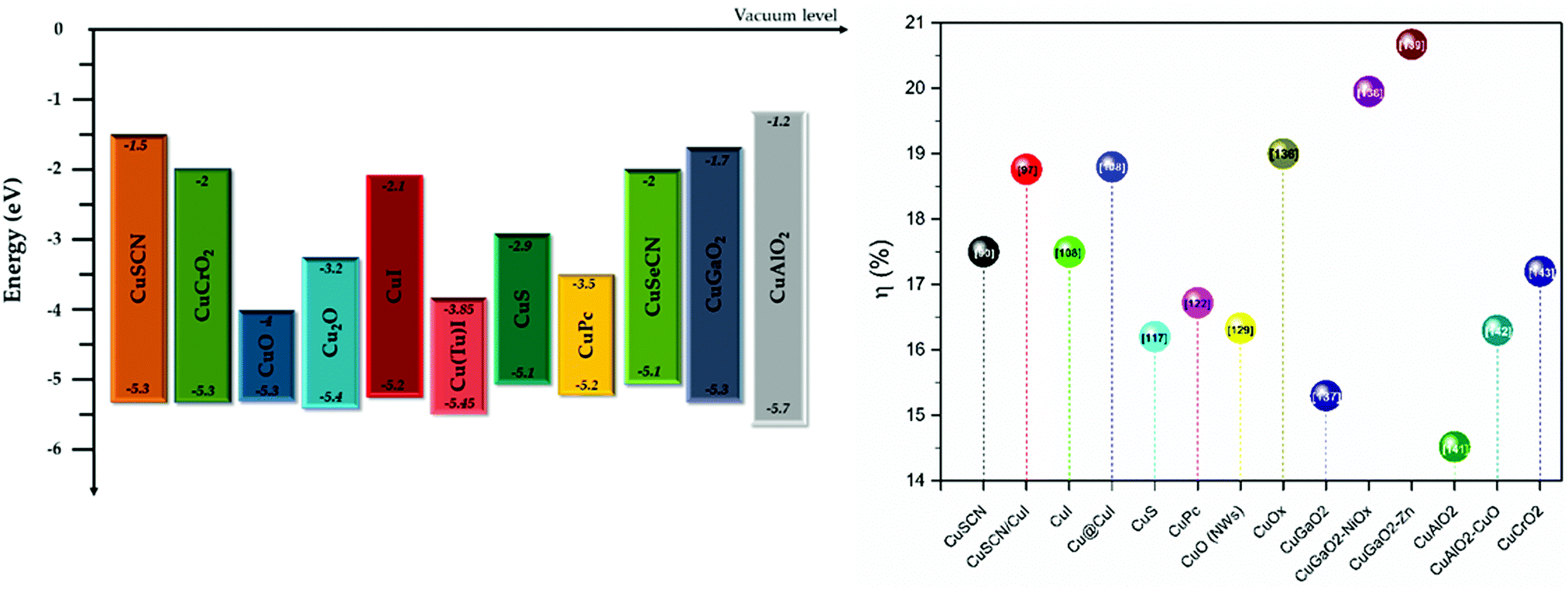 | ||
| Fig. 26 Energy levels of the Cu-based materials discussed in this review (left) and graph of power conversion efficiencies for each material, with the corresponding reference number (right). | ||
In this work, the dependence of the energy levels and phase compositions of CuyCrzO2 films on the different Cu acetylacetonate (y)/chromium acetylacetonate (z) volume ratios in the reacting solution precursors has been investigated and Cr-terminated polar CuCrO2 has been shown to provide CuyCrzO2 films with superior wettability and compatibility with perovskite precursor solution, enabling the formation of high coverage uniform perovskite films. The binary metal oxide HTL shows superior PSC performance over the mono-metal oxide HTL, and CH3NH3PbI3 perovskite based devices have led to efficiencies of 17.19% in rigid and 15.63% in flexible devices (Table 5).
| Cu based material | Perovskite | ETL | PCE [%] | Ref. |
|---|---|---|---|---|
| CuSCN | CH3NH3PbI3 | PC60BM | 17.50 | 90 |
| CuSCN/CuI | CH3NH3PbI3 | PC61BM | 18.76 | 97 |
| CuI | Cs5(MA0.17FA0.83)95Pb(I0.83Br0.17)3 | PC71BM | 17.50 | 108 |
| Cu@CuI | Cs5(MA0.17FA0.83)5Pb(I0.83Br0.17)3 | ZnO/PC71BM | 18.80 | 108 |
| CuS | CH3NH3PbI3 | C60 | 16.20 | 117 |
| CuPc | Cs0.05FA0.81MA0.14PbI2.55Br0.45 | C60 | 16.72 | 122 |
| CuO NWs | CH3NH3PbI3 | PC61BM | 16.35 | 129 |
| CuOx | CH3NH3PbI3−xClx | PC61BM/C60 | 19.00 | 136 |
| CuGaO2 | CH3NH3PbI3 | PC70BM | 15.30 | 137 |
| CuGaO2–NiOx | Csy(CH3(NH2)2)1yPb(BrxI1−x)3 | PC61BM | 19.95 | 138 |
| CuGaO2–Zn | (Cs0.15FA0.85)Pb(I0–9Br0.1)3 | PC61BM | 20.67 | 139 |
| CuAlO2 | CH3NH3PbI3−xClx | PC61BM | 14.52 | 141 |
| CuAlO2–CuO | CH3NH3PbI3 | PC70BM | 16.30 | 142 |
| CuCrO2 | CH3NH3PbI3 | PC61BM | 17.20 | 143 |
Moving one step further, in order to optimize the electrical properties of delafossite materials and increase their conductivity, by doping MIII atoms, Jeong et al.144 presented Mg doped CuCrO2 with a high conductivity of 220 S cm−1, this value being higher than those of other delafossite materials such as Mg:CuAlO2 (8 × 10⁻² S cm−1)145 and Fe:CuGaO2 (1 S cm−1).146 The as-prepared Mg-doped CuCrO2 nanocrystalline particulate films were used as HTLs in PSCs with the FTO/CH3NH3PbI3/PC61BM/BCP/Ag structure, which presented a mediocre PCE of 13.1%; however the enhanced photocurrent density values that were obtained, combined with the significantly increased stability of the devices, compared to the reference PEDOT:PSS device, still render this material promising after optimization.
There have also been reports on other Cu-based HTMs, such as Cu2ZnSnS4, Cu2BaSnS4 and Cu3SbS4, that have been used in both normal and inverted structure PSCs; however the efficiency of the resulting devices still remains low (<10%),147–149 while the energy levels of these materials present mismatches with the most commonly used perovskites (such as MAPbI3), implying the need for structural and interface engineering in order for them to be efficient.
4. Conclusion and outlook
In their simplest definition, PSCs are described as perovskite sandwiched between ETL and HTL. Serving as a major component of PSCs, the HTL has a significant influence on light harvesting, carrier extraction and transport, perovskite crystallization, stability, and cost of PSCs. With more characteristics being identified, research of PSCs shows a rising concern for high stability and low cost.In this review we have summarized the latest advances in hole transport materials based on Cu and their application in inverted structure PSCs. The research interest in this topic is continuously growing and many novel fabrication techniques and material combinations have been demonstrated. This arises from the materials’ favorable properties, combined with the ease of electrode preparation, through solution-based techniques which are applicable in large area devices. At the same time, the structure of p-i-n PSCs itself is favorable for a variety of deposition techniques, since, contrary to the normal structure counterpart, the HTL is deposited directly on a substrate, thus not affecting the perovskite film. While Cu based HTMs have shown significant advance in the normal structure PSCs, achieving high PCEs and good stability, their potential is highlighted in the inverted structure PSCs, where the great flexibility of deposition methods provides a broad range of applications. A representative example is the demonstrated application of Cu HTMs (CuSCN and CuPc) in high efficiency and stability p-i-n PSCs, processed from aqueous media, a method that is forbidden from being applied in normal structure devices, since this would cause the immediate destruction of the perovskite film.90,123
As demonstrated in Section 3, Cu derivatives are able to achieve devices with PCEs that compete with those offered by the typical organic HTMs that have been used so far, while at the same time exhibiting higher stability and reduced cost. In addition, their energy levels can be easily tailored to match all of the different perovskite compositions, rendering these materials appropriate for a wide range of applications, such as light emission and lasing, apart from solar cells.
CuSCN has led to the highest performing devices, with great stability records, especially in normal structure PSCs. The main drawback of this material is its low solubility in most organic solvents, while strong solvents, such as diethylsulfide (DES), that have been used can destroy the underlying perovskite layer. This problem is eliminated by moving to the inverted structure; however the use of strong solvents, especially the sulfur containing ones, should be eliminated when working in inert atmosphere conditions, namely inside a glove box, since they can have detrimental effects on the reactor and sensors of the box. An additional advantage of the p-i-n structure, in this direction, is that the HTL, being deposited before the perovskite layer, can be prepared in ambient conditions. In that way, by investigating a variety of solvents and precursor compositions, highly efficient electrodes, with adjustable properties, can be fabricated. A first promising result in this context has been demonstrated by Anthopoulos et al.,90 while there is still plenty of room for improvements and for the maximum exploitation of the excellent properties of CuSCN as a hole transporter. In addition, a variety of complexes of Cu with the cyanide (CN) ion, such as SeCN, as well as a combination of CuSCN with other –SCN bearing salts (e.g. KSCN) and doping with 2D materials and GRMs (graphene related materials) can deliver interesting results in terms of PCE and stability, making this group of materials worth for further study.
Even though the reports of inverted PSCs incorporating CuI as a HTL and with a PCE exceeding 15% are few, the achieving of an open circuit voltage of 1.1 V by combining it with thiourea is a clear indication that this material is capable of achieving high VOC values, under appropriate modifications, with organosulfur compounds or amides and after its conjugation with other Cu based materials. These modifications should be targeted in increasing the trap-state passivation, which at the same time will reduce the recombination rate, thus leading to the high VOC values expected. A significantly favorable property of CuI is that it can be easily deposited to form homogeneous films with a variety of simple techniques, which are compatible with large area applications.
CuS has been long established as a highly efficient counter electrode in solar cells, owing to its high electrocatalytic activity and metallic character. Even though it is able to deliver an efficient p-type electrode for inverted PSCs, its most promising potential comes from the ability to modify the transparent conductive oxide (TCO) ITO/FTO and even replace it in efficient and very low cost TCO free devices.
In general, the presence of transition metals in the structure of organometallic HTMs, like CuPc, is a critical issue because these elements can lead to toxicity and carcinogenicity, which potentially cause health problems. In addition, the poor solubility of unmodified CuPc in the most common organic solvents restricts its application in solution-processable PSCs. CuPc has been scarcely used in inverted PSCs, and one of its drawbacks when implemented in devices is that it does not perform well if not doped. Even though the doped CuPc devices that have been mentioned have achieved PCE values >16% and some impressive results of flexible devices have been demonstrated, the need for doping is an inhibitory factor for their further application in p-i-n PSCs. Even though CuPc is characterized by high hole mobility, which results in PCEs of undoped CuPc based devices of the order of 16%, when combined with the appropriate ETL (e.g. C60), the highest efficiencies are being delivered by the equivalent doped material. This is a result of a better CuPc/perovskite interface that is formed. The improvement of this interface is attributed to the beneficial effects of the dopants on the solubility of the material in organic solvents, in most of which CuPc is not soluble. In addition, dopants contribute to the increased wettability of the corresponding films’ surface, which allows for the optimized deposition of perovskites, in pinhole, homogeneous layers. In that way, by increasing both the solubility of CuPc (e.g. with alkyl chain substitution) and the better film formation ability, new, solvent based deposition techniques can be investigated, eliminating the most commonly used vacuum evaporation, which has been shown to be not ideal for thin film applications.
Finally, a great potential exists for the Cu oxide group of materials, namely cupric oxide (CuO) and cuprous oxide (Cu2O), which are established as efficient p-type semiconductors for solar cell applications, yielding high photovoltage values. Even though the PCEs of the devices that have been reported so far are very mediocre, further research on these materials could lead to significant improvements. A big advantage of Cu based oxides is their controllable synthesis procedures, which gives a wide range of electrode preparation methods, that can, in turn, be tuned according to the application prospects and the desirable properties. In addition, further doping and mixing with other oxides, in single or multilayered configuration electrodes, open new roads towards high efficiency, low-cost PSCs.
As a general view, the devices based on Cu based HTMs have recently demonstrated PCEs over 20%, which are comparable to PCEs of devices based on organic HTMs. Most importantly, the stability of PCSs is much improved by the Cu based HTM. However, there remain some drawbacks to be tackled. To start with, the balance between perovskite and HTM is very important, rather than focusing only on the selective contact materials. Type II band alignment is highly desired, since it is favorable for efficient hole extraction. It is necessary to find a suitable perovskite material with appropriate band alignment with the Cu based materials, or to engineer the interfaces to ensure enough hole extraction driving force and inhibit back electron transfer. To further enhance the performance of inverted planar PSCs, the fabrication of a compact and pinhole-free Cu HTM layer is of great importance to effectively avoid direct contact between the ITO electrode and the perovskite layer and thus a leakage path. Interface engineering between the inorganic HTM and the perovskite layer, such as trap-state passivation, would be an effective strategy to lower charge-recombination losses and thus to further improve the performance. In addition, the PCE significantly depends on the preparation methods of the HTM layer. The templating role of the HTL needs to be considered carefully for further PCE optimization of inverted PSCs. Many researchers have highlighted the critical function of the template in the process of nucleation and crystal growth of high-quality perovskite grains. Finally, the interface degradation problem should be resolved, possibly with the development of novel interface engineering. Overall, there is plenty of room for improvement when moving from organic HTLs to Cu based HTLs, which is in a direct relation to the different type of material to be used. Depending on the material, this would be the energy band alignment, the deposition method, the interface stability or a combination of all.
To conclude, the most promising Cu based HTM that has been reported so far is CuSCN in terms of efficiency values that it can deliver; however in terms of ease of fabrication, the iodide and oxide counterparts dominate. There is still plenty of room for improvement, by exploring more Cu based materials as hole transporters in PSCs and by testing the already reported ones regarding their stability, with respect to both small and large area devices.
Having all the aforementioned in mind, it is safe to say that Cu based materials represent a new class of highly promising inorganic hole transport materials that can lead to the realization of inverted PSCs with high PCE and increased stability, with a low cost. Further research at both material and device engineering level could lead to impressive results that will push the potential of perovskites one more step further towards their commercialization.
Conflicts of interest
There are no conflicts to declare.Acknowledgements
This research has been co-financed by the European Union and Greek national funds through the Operational Program Competitiveness, Entrepreneurship and Innovation, under the call RESEARCH – CREATE – INNOVATE (project code: T1EDK-01082).References
- A. Kojima, K. Teshima, Y. Shirai and T. Miyasaka, Organometal Halide Perovskites as Visible-Light Sensitizers for Photovoltaic Cells, J. Am. Chem. Soc., 2009, 131(17), 6050–6051, DOI:10.1021/ja809598r.
- M. Saliba, J. P. Correa-Baena, C. M. Wolff, M. Stolterfoht, N. Phung, S. Albrecht, D. Neher and A. Abate, How to Make over 20% Efficient Perovskite Solar Cells in Regular (n-i-p) and Inverted (p-i-n) Architectures, Chem. Mater., 2018, 30(13), 4193–4201, DOI:10.1021/acs.chemmater.8b00136.
- Y. Hassan, Y. Song, R. D. Pensack, A. I. Abdelrahman, Y. Kobayashi, M. A. Winnik and G. D. Scholes, Structure-Tuned Lead Halide Perovskite Nanocrystals, Adv. Mater., 2016, 28(3), 566–573, DOI:10.1002/adma.201503461.
- G. Grancini, C. Roldán-Carmona, I. Zimmermann, E. Mosconi, X. Lee, D. Martineau, S. Narbey, F. Oswald, F. De Angelis and M. Graetzel, et al., One-Year Stable Perovskite Solar Cells by 2D/3D Interface Engineering, Nat. Commun., 2017, 8, 1–8, DOI:10.1038/ncomms15684.
- L. Meng, C. Sun, R. Wang, W. Huang, Z. Zhao, P. Sun, T. Huang, J. Xue, J.-W. Lee, C. Zhu, Y. Huang, Y. Li and Y. Yang, Tailored Phase Conversion under Conjugated Polymer Enables Thermally Stable Perovskite Solar Cells with Efficiency Exceeding 21%, J. Am. Chem. Soc., 2018, 140(49), 17255–17262, DOI:10.1021/jacs.8b10520.
- Y. Ko, C. Kim, C. Lee, Y. Kim and Y. Jun, Investigation of Hole-Transporting Poly(Triarylamine) (PTAA) on Aggregation and Charge Transport for Hysteresis-Less Scalable Planar Perovskite Solar Cells, ACS Appl. Mater. Interfaces, 2018, 10(14), 11633–11641, DOI:10.1021/acsami.7b18745.
- R. Hu, R. Zhang, Y. Ma, W. Liu, L. Chu, W. Mao and J. Zhang, Enhanced Hole Transfer in Hole-Conductor-Free Perovskite Solar Cells via Incorporating CuS into Carbon Electrodes, Appl. Surf. Sci., 2018, 462, 840–846, DOI:10.1016/j.apsusc.2018.08.078.
- X. Yin, Y. Zhou, J. Han, H. Nan, M. Tai and Y. Gu, Highly Efficient Inverted Perovskite Solar Cells Based on Self-Assembled Graphene Derivatives, J. Mater. Chem. A, 2018, 6, 20702–20711, 10.1039/C8TA05955A.
- J. Chen, S. Kim and N. Park, FA0.88Cs0.12PbI3−x(PF6)x Interlayer Formed by Ion ExchangeReaction between Perovskite and Hole Transporting Layer for Improving Photovoltaic Performance and Stability, Adv. Mater., 2018, 1801948, 1–11, DOI:10.1002/adma.201801948.
- N. J. Jeon, H. Na, E. H. Jung, T. Y. Yang, Y. G. Lee, G. Kim, H. W. Shin, S. Il Seok, J. Lee and J. Seo, A Fluorene-Terminated Hole-Transporting Material for Highly Efficient and Stable Perovskite Solar Cells, Nat. Energy, 2018, 3(8), 682–689, DOI:10.1038/s41560-018-0200-6.
- E. Kymakis, Interfacial Engineering of Perovskite Solar Cells for Improved Performance and Stability, Adv. Mater. Interfaces, 2018, 5(22), 1801595, DOI:10.1002/admi.201801595.
- G. Kakavelakis, E. Kymakis and K. Petridis, 2D Materials Beyond Graphene for Metal Halide Perovskite Solar Cells, Adv. Mater. Interfaces, 2018, 5(22), 1800339, DOI:10.1002/admi.201800339.
- G. Kakavelakis, K. Petridis and E. Kymakis, Recent Advances in Plasmonic Metal and Rare-Earth-Element Upconversion Nanoparticle Doped Perovskite Solar Cells, J. Mater. Chem. A, 2017, 5(41), 21604–21624, 10.1039/C7TA05428A.
- (a) A. Agresti, S. Pescetelli, A. L. Palma, A. E. Del Rio Castillo, D. Konios, G. Kakavelakis, S. Razza, L. Cinà, E. Kymakis and F. Bonaccorso, et al., Graphene Interface Engineering for Perovskite Solar Modules: 12.6% Power Conversion Efficiency over 50 C m2 Active Area, ACS Energy Lett., 2017, 2(1), 279–287, DOI:10.1021/acsenergylett.6b00672; (b) C. Zuo, H. J. Bolink, H. Han, J. Huang, D. Cahen and L. Ding, Advances in Perovskite Solar Cells, Adv. Sci., 2016, 3(7), 1500324, DOI:10.1002/advs.201500324; (c) Q. Zeng, L. Liu, Z. Xiao, F. Liu, Y. Hua, Y. Yuan and L. Ding, Sci. Bull., 2019, 64(13), 885–887, DOI:10.1016/j.scib.2019.05.015.
- G. Grancini, C. Roldán-Carmona, I. Zimmermann, E. Mosconi, X. Lee, D. Martineau, S. Narbey, F. Oswald, F. De Angelis and M. Graetzel, et al., One-Year Stable Perovskite Solar Cells by 2D/3D Interface Engineering, Nat. Commun., 2017, 8, 15684 CrossRef CAS PubMed.
- A Decade of Perovskite Photovoltaics, Nat. Energy, 2019, 4(1), 1, DOI:10.1038/s41560-018-0323-9.
- J. M. Ball, M. M. Lee, A. Hey and H. J. Snaith, Low-Temperature Processed Meso-Superstructured to Thin-Film Perovskite Solar Cells, Energy Environ. Sci., 2013, 6(6), 1739–1743, 10.1039/C3EE40810H.
- S. D. Stranks, G. E. Eperon, G. Grancini, C. Menelaou, M. J. P. Alcocer, T. Leijtens, L. M. Herz, A. Petrozza and H. J. Snaith, Electron-Hole Diffusion Lengths Exceeding 1 Micrometer in an Organometal Trihalide Perovskite Absorber, Science, 2013, 342(6156), 341–344, DOI:10.1126/science.1243982.
- G. Xing, N. Mathews, S. Sun, S. S. Lim, Y. M. Lam, M. Grätzel, S. Mhaisalkar and T. C. Sum, Long-Range Balanced Electron- and Hole-Transport Lengths in Organic-Inorganic CH3NH3PbI3, Science, 2013, 342(6156), 344–347, DOI:10.1126/science.1243167.
- J. Y. Jeng, Y. F. Chiang, M. H. Lee, S. R. Peng, T. F. Guo, P. Chen and T. C. Wen, CH3NH3PbI3 Perovskite/Fullerene Planar-Heterojunction Hybrid Solar Cells, Adv. Mater., 2013, 25(27), 3727–3732, DOI:10.1002/adma.201301327.
- T. Liu, K. Chen, Q. Hu, R. Zhu and Q. Gong, Inverted Perovskite Solar Cells: Progresses and Perspectives, Adv. Energy Mater., 2016, 6(17), 1600457, DOI:10.1002/aenm.201600457.
- A. Kojima, K. Teshima, Y. Shirai and T. Miyasaka, Organometal Halide Perovskites as Visible-Light Sensitizers for Photovoltaic Cells, J. Am. Chem. Soc., 2009, 131(17), 6050–6051, DOI:10.1021/ja809598r.
- G. E. Eperon, S. D. Stranks, C. Menelaou, M. B. Johnston, L. M. Herz and H. J. Snaith, Formamidinium Lead Trihalide: A Broadly Tunable Perovskite for Efficient Planar Heterojunction Solar Cells, Energy Environ. Sci., 2014, 7(3), 982–988, 10.1039/c3ee43822h.
- J. W. Lee, D. H. Kim, H. S. Kim, S. W. Seo, S. M. Cho and N. G. Park, Formamidinium and Cesium Hybridization for Photo- and Moisture-Stable Perovskite Solar Cell, Adv. Energy Mater., 2015, 5(20), 1501310, DOI:10.1002/aenm.201501310.
- M. Saliba, J.-P. Correa-Baena, M. Graetzel, A. Hagfeldt and A. Abate, Perovskite Solar Cells from the Atomic to the Film Level, Angew. Chem., Int. Ed., 2017, 57(10), 2554–2569, DOI:10.1002/anie.201703226.
- Ç. Odabaşı Özer and R. Yıldırım, Performance Analysis of Perovskite Solar Cells in 2013–2018 Using Machine-Learning Tools, Nano Energy, 2019, 56, 770–791, DOI:10.1016/j.nanoen.2018.11.069.
- D. Yang, T. Sano, Y. Yaguchi, H. Sun, H. Sasabe and J. Kido, Achieving 20% Efficiency for Low-Temperature-Processed Inverted Perovskite Solar Cells, Adv. Funct. Mater., 2018, 1807556, 1–6, DOI:10.1002/adfm.201807556.
- X. Liu, Y. Cheng, C. Liu, T. Zhang, N. Zhang, S. Zhang, J. Chen, Q. Xu, J. Ouyang and H. Gong, 20.7% Highly Reproducible Inverted Planar Perovskite Solar Cells with Enhanced Fill Factor and Eliminated Hysteresis, Energy Environ. Sci., 2019, 12, 1622–1633, 10.1039/C9EE00872A.
- F. H. Isikgor, B. Li, H. Zhu, Q. Xu and J. Ouyang, High Performance Planar Perovskite Solar Cells with a Perovskite of Mixed Organic Cations and Mixed Halides, MA1−xFAxPbI3−yCly, J. Mater. Chem. A, 2016, 4(32), 12543–12553, 10.1039/c6ta03381d.
- J. You, Y. (Michael) Yang, Z. Hong, T.-B. Song, L. Meng, Y. Liu, C. Jiang, H. Zhou, W.-H. Chang and G. Li, et al., Moisture Assisted Perovskite Film Growth for High Performance Solar Cells, Appl. Phys. Lett., 2014, 105(18), 183902, DOI:10.1063/1.4901510.
- D. Luo, W. Yang, Z. Wang, A. Sadhanala, Q. Hu, R. Su, R. Shivanna, G. F. Trindade, J. F. Watts, Z. Xu, T. Liu, K. Chen, F. Ye, P. Wu, L. Zhao, J. Wu, Y. Tu, Y. Zhang, X. Yang, W. Zhang, R. H. Friend, Q. Gong, H. J. Snaith and R. Zhu, Enhanced Photovoltage for Inverted Planar Heterojunction Perovskite Solar Cells, Science, 2018, 1446, 1442–1446, DOI:10.1126/science.aap9282.
- M. Stolterfoht, C. M. Wolff, J. A. Marquez, S. Zhang, C. J. Hages, D. Rothhardt, S. Albrecht, P. L. Burn, P. Meredith, T. Unold and D. Neher, Visualization and Suppression of Interfacial Recombination for High-Efficiency Large-Area pin Perovskite Solar Cells, Nat. Energy, 2018, 3, 847–854, DOI:10.1038/s41560-018-0219-8.
- X. Zheng, B. Chen, J. Dai, Y. Fang, Y. Bai, Y. Lin, H. Wei, X. C. Zeng and J. Huang, Defect Passivation in Hybrid Perovskite Solar Cells Using Quaternary Ammonium Halide Anions and Cations, Nat. Energy, 2017, 2(7), 17102, DOI:10.1038/nenergy.2017.102.
- J. C. Yu, S. Badgujar, E. D. Jung, V. K. Singh, D. W. Kim, J. Gierschner, E. Lee, Y. S. Kim, S. Cho and M. S. Kwon, et al., Highly Efficient and Stable Inverted Perovskite Solar Cell Obtained via Treatment by Semiconducting Chemical Additive, Adv. Mater., 2019, 31(6), 1–10, DOI:10.1002/adma.201805554.
- M. Powalla, S. Paetel, E. Ahlswede, R. Wuerz, C. D. Wessendorf and T. Magorian Friedlmeier, Thin-Film Solar Cells Exceeding 22% Solar Cell Efficiency: An Overview on CdTe-, Cu(In,Ga)Se2-, and Perovskite-Based Materials, Appl. Phys. Rev., 2018, 5(4), 041602, DOI:10.1063/1.5061809.
- D. Yang, J. Lv, X. Zhao, Q. Xu, Y. Fu, Y. Zhan, A. Zunger and L. Zhang, Functionality-Directed Screening of Pb-Free Hybrid Organic–Inorganic Perovskites with Desired Intrinsic Photovoltaic Functionalities, Chem. Mater., 2017, 29(2), 524–538, DOI:10.1021/acs.chemmater.6b03221.
- J.-W. Shin, H. Cho, J. Lee, J. Moon, J.-H. Han, K. Kim, S. Cho, J.-I. Lee, B.-H. Kwon and D.-H. Cho, et al., Overcoming the Efficiency Limit of Organic Light-Emitting Diodes Using Ultra-Thin and Transparent Graphene Electrodes, Opt. Express, 2018, 26(2), 617–626, DOI:10.1364/OE.26.000617.
- S. Chen, Q. Zhang, W. Shang, L. Liu, H. Yu and S. Zhang, Interfacial Engineering of Graphene for Highly Efficient Blue and White Organic Light-Emitting Devices, Sci. Rep., 2018, 1–9, DOI:10.1038/s41598-018-26464-8.
- L. Liu, W. Shang, C. Han, Q. Zhang, Y. Yao, X. Ma, M. Wang, H. Yu, Y. Duan and J. Sun, et al., Two-In-One Method for Graphene Transfer: Simplified Fabrication Process for Organic Light-Emitting Diodes, ACS Appl. Mater. Interfaces, 2018, 10(8), 7289–7295, DOI:10.1021/acsami.7b19039.
- H. D. Kim, H. Ohkita, H. Benten and S. Ito, Photovoltaic Performance of Perovskite Solar Cells with Different Grain Sizes, Adv. Mater., 2016, 28(5), 917–922, DOI:10.1002/adma.201504144.
- D. Liu, Y. Li, J. Yuan, Q. Hong, G. Shi, D. Yuan, J. Wei, C. Huang, J. Tang and M. K. Fung, Improved Performance of Inverted Planar Perovskite Solar Cells with F4-TCNQ Doped PEDOT:PSS Hole Transport Layers, J. Mater. Chem. A, 2017, 5(12), 5701–5708, 10.1039/C6TA10212C.
- (a) L. Hu, K. Sun, M. Wang, W. Chen, B. Yang, J. Fu, Z. Xiong, X. Li, X. Tang and Z. Zang, et al., Inverted Planar Perovskite Solar Cells with a High Fill Factor and Negligible Hysteresis by the Dual Effect of NaCl-Doped PEDOT:PSS, ACS Appl. Mater. Interfaces, 2017, 9(50), 43902–43909, DOI:10.1021/acsami.7b14592; (b) C. Zuo, D. Vak, D. Angmo, L. Ding and M. Gao, One-step roll-to-roll air processed high efficiency perovskite solar cells, Nano Energy, 2018, 46, 185–192, DOI:10.1016/j.nanoen.2018.01.037.
- H. Guo, X. Huang, B. Pu, J. Yang, H. Chen, Y. Zhou, J. Yang, Y. Li, Z. Wang and X. Niu, Efficiency Enhancement in Inverted Planar Perovskite Solar Cells by Synergetic Effect of Sulfated Graphene Oxide (SGO) and PEDOT:PSS as Hole Transporting Layer, RSC Adv., 2017, 7(79), 50410–50419, 10.1039/c7ra10113a.
- W. S. Yang, J. H. Noh, N. J. Jeon, Y. C. Kim, S. Ryu, J. Seo and S. I. Seok, High-Performance Photovoltaic Perovskite Layers Fabricated through Intramolecular Exchange, Science, 2015, 348(6240), 1234–1237, DOI:10.1126/science.aaa9272.
- F. Xie, C.-C. Chen, Y. Wu, X. Li, M. Cai, X. Liu, X. Yang and L. Han, Vertical Recrystallization for Highly Efficient and Stable Formamidinium-Based Inverted-Structure Perovskite Solar Cells, Energy Environ. Sci., 2017, 10(9), 1942–1949, 10.1039/C7EE01675A.
- Q. Fu, S. Xiao, X. Tang and T. Hu, High-Performance Inverted Planar Perovskite Solar Cells Based on Solution-Processed Rubidium-Doped Nickel Oxide Hole-Transporting Layer, Org. Electron., 2019, 69, 34–41, DOI:10.1016/j.orgel.2019.03.004.
- A. Corani, M.-H. Li, P.-S. Shen, P. Chen, T.-F. Guo, A. El Nahhas, K. Zheng, A. Yartsev, V. Sundström and C. S. Ponseca, Ultrafast Dynamics of Hole Injection and Recombination in Organometal Halide Perovskite Using Nickel Oxide as P-Type Contact Electrode, J. Phys. Chem. Lett., 2016, 7(7), 1096–1101, DOI:10.1021/acs.jpclett.6b00238.
- W. Nie, H. Tsai, J. C. Blancon, F. Liu, C. C. Stoumpos, B. Traore, M. Kepenekian, O. Durand, C. Katan and S. Tretiak, et al., Critical Role of Interface and Crystallinity on the Performance and Photostability of Perovskite Solar Cell on Nickel Oxide, Adv. Mater., 2018, 30(5), 1–9, DOI:10.1002/adma.201703879.
- Y. Wei, K. Yao, X. Wang, Y. Jiang, X. Liu, N. Zhou and F. Li, Improving the Efficiency and Environmental Stability of Inverted Planar Perovskite Solar Cells via Silver-Doped Nickel Oxide Hole-Transporting Layer, Appl. Surf. Sci., 2018, 427, 782–790, DOI:10.1016/j.apsusc.2017.08.184.
- S. Teo, Z. Guo, Z. Xu, C. Zhang, Y. Kamata, S. Hayase and T. Ma, The Role of Lanthanum in a Nickel Oxide-Based Inverted Perovskite Solar Cell for Efficiency and Stability Improvement, ChemSusChem, 2019, 12(2), 518–526, DOI:10.1002/cssc.201802231.
- R. Kaneko, T. H. Chowdhury, G. Wu, M. E. Kayesh, S. Kazaoui, K. Sugawa, J. J. Lee, T. Noda, A. Islam and J. Otsuki, Cobalt-Doped Nickel Oxide Nanoparticles as Efficient Hole Transport Materials for Low-Temperature Processed Perovskite Solar Cells, Sol. Energy, 2019, 181, 243–250, DOI:10.1016/j.solener.2019.01.097.
- Q. He, K. Yao, X. Wang, X. Xia, S. Leng and F. Li, Room-Temperature and Solution-Processable Cu-Doped Nickel Oxide Nanoparticles for Efficient Hole-Transport Layers of Flexible Large-Area Perovskite Solar Cells, ACS Appl. Mater. Interfaces, 2017, 9(48), 41887–41897, DOI:10.1021/acsami.7b13621.
- C. Duan, M. Zhao, C. Zhao, Y. Wang, J. Li, W. Han, Q. Hu, L. Yao, H. Jian and F. Lu, et al., Inverted CH3NH3PbI3 Perovskite Solar Cells Based on Solution-Processed V2O5 Film Combined with P3CT Salt as Hole Transport Layer. Mater. Today, Energy, 2018, 9, 487–495, DOI:10.1016/j.mtener.2018.07.004.
- H. Sung, N. Ahn, M. S. Jang, J. K. Lee, H. Yoon, N. G. Park and M. Choi, Transparent Conductive Oxide-Free Graphene-Based Perovskite Solar Cells with over 17% Efficiency, Adv. Energy Mater., 2016, 6(3), 2–7, DOI:10.1002/aenm.201501873.
- Z. Li, Stable Perovskite Solar Cells Based on WO3 Nanocrystals as Hole Transport Layer, Chem. Lett., 2015, 44(8), 1140–1141, DOI:10.1246/cl.150445.
- T. Stubhan, N. Li, N. A. Luechinger, S. C. Halim, G. J. Matt and C. J. Brabec, High Fill Factor Polymer Solar Cells Incorporating a Low Temperature Solution Processed WO3 Hole Extraction Layer, Adv. Energy Mater., 2012, 2(12), 1433–1438, DOI:10.1002/aenm.201200330.
- Y. Wang and T. W. Hamann, Improved Performance Induced by In Situ Ligand Exchange Reactions of Copper Bipyridyl Redox Couples in Dye-Sensitized Solar Cells, Chem. Commun., 2018, 54(87), 12361–12364, 10.1039/C8CC07191H.
- A. Büttner, Y. S. Brauchli, C. E. Constable and E. C. Housecroft, Effects of Introducing Methoxy Groups into the Ancillary Ligands in Bis(Diimine) Copper(I) Dyes for Dye-Sensitized Solar Cells, Inorganics, 2018, 6(2), 40, DOI:10.3390/inorganics6020040.
- A. H. Alami, B. Rajab, J. Abed, M. Faraj, A. A. Hawili and H. Alawadhi, Investigating Various Copper Oxides-Based Counter Electrodes for Dye Sensitized Solar Cell Applications, Energy, 2019, 174, 526–533, DOI:10.1016/j.energy.2019.03.011.
- C. Dragonetti, M. Magni, A. Colombo, F. Fagnani, D. Roberto, F. Melchiorre, P. Biagini and S. Fantacci, Towards Efficient Sustainable Full-Copper Dye-Sensitized Solar Cells, Dalton Trans., 2019, 48, 9703–9711, 10.1039/C9DT00790C.
- N. Vlachopoulos, M. Freitag and A. Hagfeldt, Cu Complex Redox Couples Open Up New Possibilities for Dye-Sensitized Solar Cells, Counter Electrodes for Dye-sensitized and Perovskite Solar Cells, 2018, pp. 349–365 DOI:10.1002/9783527813636.ch14.
- Y. Cao, Y. Saygili, A. Ummadisingu, J. Teuscher, J. Luo, N. Pellet, F. Giordano, S. M. Zakeeruddin, J.-E. Moser and M. Freitag, et al., 11% Efficiency Solid-State Dye-Sensitized Solar Cells with Copper(II/I) Hole Transport Materials, Nat. Commun., 2017, 8, 15390 CrossRef PubMed.
- Z. Pan, H. Rao, I. Mora-Seró, J. Bisquert and X. Zhong, Quantum Dot-Sensitized Solar Cells, Chem. Soc. Rev., 2018, 47(20), 7659–7702, 10.1039/c8cs00431e.
- H. Tan, A. Jain, O. Voznyy, X. Lan, F. P. García de Arquer, J. Z. Fan, R. Quintero-Bermudez, M. Yuan, B. Zhang and Y. Zhao, et al., Efficient and Stable Solution-Processed Planar Perovskite Solar Cells via Contact Passivation, Science, 2017, 355(6326), 722–726, DOI:10.1126/science.aai9081.
- J. H. Heo, H. J. Han, D. Kim, T. K. Ahn and S. H. Im, Hysteresis-Less Inverted CH3NH3PbI3 Planar Perovskite Hybrid Solar Cells with 18.1% Power Conversion Efficiency, Energy Environ. Sci., 2015, 8(5), 1602–1608, 10.1039/C5EE00120J.
- B. Ding, Y. Li, S.-Y. Huang, Q.-Q. Chu, C.-X. Li, C.-J. Li and G.-J. Yang, Material Nucleation/Growth Competition Tuning towards Highly Reproducible Planar Perovskite Solar Cells with Efficiency Exceeding 20%, J. Mater. Chem. A, 2017, 5(15), 6840–6848, 10.1039/C7TA00027H.
- M. Yang, Z. Li, M. O. Reese, O. G. Reid, D. H. Kim, S. Siol, T. R. Klein, Y. Yan, J. J. Berry and M. F. A. M. Van Hest, et al., Perovskite Ink with Wide Processing Window for Scalable High-Efficiency Solar Cells, Nat. Energy, 2017, 2(5), 1–9, DOI:10.1038/nenergy.2017.38.
- N. Yaghoobi Nia, M. Zendehdel, L. Cinà, F. Matteocci and A. Di Carlo, A Crystal Engineering Approach for Scalable Perovskite Solar Cells and Module Fabrication: A Full out of Glove Box Procedure, J. Mater. Chem. A, 2018, 6(2), 659–671, 10.1039/C7TA08038G.
- W. S. Yang, B. W. Park, E. H. Jung, N. J. Jeon, Y. C. Kim, D. U. Lee, S. S. Shin, J. Seo, E. K. Kim and J. H. Noh, et al., Iodide Management in Formamidinium-Lead-Halide-Based Perovskite Layers for Efficient Solar Cells, Science, 2017, 356(6345), 1376–1379, DOI:10.1126/science.aan2301.
- X. Li, X. Li, D. Bi, C. Yi, J. Décoppet, J. Luo, S. M. Zakeeruddin, A. Hagfeldt and M. Grätzel, A Vacuum Flash – Assisted Solution Process for High-Efficiency Large-Area Perovskite Solar Cells, Science, 2016, 353(6294), 58–62, DOI:10.1126/science.aaf8060.
- Y. Wu, X. Yang, W. Chen, Y. Yue, M. Cai, F. Xie, E. Bi, A. Islam and L. Han, Perovskite Solar Cells with 18.21% Efficiency and Area over 1Cm2 Fabricated by Heterojunction Engineering, Nat. Energy, 2016, 1, 16148, DOI:10.1038/nenergy.2016.148.
- W. Chen, Y. Wu, Y. Yue, J. Liu, W. Zhang, X. Yang, H. Chen, E. Bi, I. Ashraful and M. Grätzel, et al., Efficient and Stable Large-Area Perovskite Solar Cells with Inorganic Charge Extraction Layers, Science, 2015, 350(6263), 944–948, DOI:10.1126/science.aad1015.
- C. H. Chiang, M. K. Nazeeruddin, M. Grätzel and C. G. Wu, The Synergistic Effect of H2O and DMF towards Stable and 20% Efficiency Inverted Perovskite Solar Cells, Energy Environ. Sci., 2017, 10(3), 808–817, 10.1039/c6ee03586h.
- S. Hong, J. Lee, H. Kang, G. Kim, S. Kee, J.-H. Lee, S. Jung, B. Park, S. Kim and H. Back, et al., High-Efficiency Large-Area Perovskite Photovoltaic Modules Achieved via Electrochemically Assembled Metal-Filamentary Nanoelectrodes, Sci. Adv., 2018, 4(8), eaat3604, DOI:10.1126/sciadv.aat3604.
- M. Yang, D. H. Kim, T. R. Klein, Z. Li, M. O. Reese, B. J. Tremolet de Villers, J. J. Berry, M. F. A. M. van Hest and K. Zhu, Highly Efficient Perovskite Solar Modules by Scalable Fabrication and Interconnection Optimization, ACS Energy Lett., 2018, 3(2), 322–328, DOI:10.1021/acsenergylett.7b01221.
- http://www.solliance.eu .
- http://www.imec-int.com .
- http://www.microquanta.com .
- H. Chen, F. Ye, W. Tang, J. He, M. Yin, Y. Wang, F. Xie, E. Bi, X. Yang and M. Grätzel, et al., A Solvent- and Vacuum-Free Route to Large-Area Perovskite Films for Efficient Solar Modules, Nature, 2017, 550, 92, DOI:10.1038/nature23877.
- A. Priyadarshi, L. J. Haur, P. Murray, D. Fu, S. Kulkarni, G. Xing, T. C. Sum, N. Mathews and S. G. Mhaisalkar, A Large Area (70 cm2) Monolithic Perovskite Solar Module with a High Efficiency and Stability, Energy Environ. Sci., 2016, 9(12), 3687–3692, 10.1039/C6EE02693A.
- Y. Hu, S. Si, A. Mei, Y. Rong, H. Liu, X. Li and H. Han, Stable Large-Area (10 × 10 cm2) Printable Mesoscopic Perovskite Module Exceeding 10% Efficiency, Sol. RRL, 2017, 1(2), 1600019, DOI:10.1002/solr.201600019.
- F. De Rossi, J. A. Baker, D. Beynon, K. E. A. Hooper, S. M. P. Meroni, D. Williams, Z. Wei, A. Yasin, C. Charbonneau and E. H. Jewell, et al., All Printable Perovskite Solar Modules with 198 cm2 Active Area and Over 6% Efficiency, Adv. Mater. Technol., 2018, 3(11), 1800156, DOI:10.1002/admt.201800156.
- http://www.toshiba.co.jp .
- Z. Li, T. R. Klein, D. H. Kim, M. Yang, J. J. Berry, M. F. A. M. Van Hest and K. Zhu, Scalable Fabrication of Perovskite Solar Cells, Nat. Rev. Mater., 2018, 3, 1–20, DOI:10.1038/natrevmats.2018.17.
- N. Arora, M. I. Dar, A. Hinderhofer, N. Pellet, F. Schreiber, S. M. Zakeeruddin and M. Grätzel, Perovskite Solar Cells with CuSCN Hole Extraction Layers Yield Stabilized Efficiencies Greater than 20%, Science, 2017, 358(6364), 768–771, DOI:10.1126/science.aam5655.
- M. Cai, Y. Wu, H. Chen, X. Yang, Y. Qiang and L. Han, Cost-Performance Analysis of Perovskite Solar Modules, Adv. Sci., 2017, 4(1), 1600269, DOI:10.1002/advs.201600269.
- Z. Yang, S. Zhang, L. Li and W. Chen, Research Progress on Large-Area Perovskite Thin Films and Solar Modules, J. Mater., 2017, 3(4), 231–244, DOI:10.1016/j.jmat.2017.09.002.
- R. D. Blue and F. C. Mathers, Electrodeposition of Metals and Alloys from Formamide Solutions, J. Electrochem. Soc., 1933, 63(1), 231–238, DOI:10.1149/1.3493815.
- N. Chaudhary, R. Chaudhary, J. P. Kesari, A. Patra and S. Chand, Copper Thiocyanate (CuSCN): An Efficient Solution-Processable Hole Transporting Layer in Organic Solar Cells, J. Mater. Chem. C, 2015, 3(45), 11886–11892, 10.1039/C5TC03124A.
- T. Du, J. Li, D. J. Payne, N. Wijeyasinghe, L. Tsetseris, H. Faber, Y.-H. Lin, P. Pattanasattayavong, F. Yan and M. A. McLachlan, et al., Copper(I) Thiocyanate (CuSCN) Hole-Transport Layers Processed from Aqueous Precursor Solutions and Their Application in Thin-Film Transistors and Highly Efficient Organic and Organometal Halide Perovskite Solar Cells, Adv. Funct. Mater., 2017, 27(35), 1701818, DOI:10.1002/adfm.201701818.
- A. Seitkhan, F. Eisner, N. Tessler, F. Yan, P. Patsalas, L. Tsetseris, J. Li, T. D. Anthopoulos, O. Solomeshch and Y.-H. Lin, et al., P-Doping of Copper(I) Thiocyanate (CuSCN) Hole-Transport Layers for High-Performance Transistors and Organic Solar Cells, Adv. Funct. Mater., 2018, 28(31), 1802055, DOI:10.1002/adfm.201802055.
- N. Arora, M. I. Dar, A. Hinderhofer, N. Pellet, F. Schreiber, S. M. Zakeeruddin and M. Grätzel, Perovskite Solar Cells with CuSCN Hole Extraction Layers Yield Stabilized Efficiencies Greater than 20%, Science, 2017, 358(6364), 768–771, DOI:10.1126/science.aam5655.
- T. H. Chowdhury, M. Akhtaruzzaman, M. E. Kayesh, R. Kaneko, T. Noda, J. J. Lee and A. Islam, Low Temperature Processed Inverted Planar Perovskite Solar Cells by R-GO/CuSCN Hole-Transport Bilayer with Improved Stability, Sol. Energy, 2018, 171, 652–657, DOI:10.1016/j.solener.2018.07.022.
- M. Lyu, J. Chen and N. Park, Improvement of efficiency and Stability of CuSCN-Based Inverted Perovskite Solar Cells by Post-Treatment with Potassium Thiocyanate, J. Solid State Chem., 2019, 269, 367–374, DOI:10.1016/j.jssc.2018.10.014.
- B. Li, X. Yao, Y. Zhao, Y. Li, S. Zhao, B. Shi, D. Zhang, G. Wang, X. Zhang and C. Wei, et al., Delayed Annealing Treatment for High-Quality CuSCN: Exploring Its Impact on Bifacial Semitransparent n-i-p Planar Perovskite Solar Cells, ACS Appl. Energy Mater., 2018, 1(4), 1575–1584, DOI:10.1021/acsaem.8b00001.
- S. Ye, H. Rao, W. Yan, Y. Li, W. Sun, H. Peng, Z. Liu, Z. Bian, Y. Li and C. Huang, A Strategy to Simplify the Preparation Process of Perovskite Solar Cells by Co-Deposition of a Hole-Conductor and a Perovskite Layer, Adv. Mater., 2016, 28(43), 9648–9654, DOI:10.1002/adma.201603850.
- H. Wang, Z. Yu, J. Lai, X. Song, X. Yang, A. Hagfeldt and L. Sun, One plus One Greater than Two: High-Performance Inverted Planar Perovskite Solar Cells Based on a Composite CuI/CuSCN Hole-Transporting Layer, J. Mater. Chem. A, 2018, 6(43), 21435–21444, 10.1039/C8TA07332E.
- Y. Liu, Z. Liu and E.-C. Lee, High-Performance Inverted Perovskite Solar Cells Using Doped Poly(Triarylamine) as the Hole Transport Layer, ACS Appl. Energy Mater., 2019, 2(3), 1932–1942, DOI:10.1021/acsaem.8b02047.
- N. Wijeyasinghe, L. Tsetseris, A. Regoutz, W. Y. Sit, Z. Fei, T. Du, X. Wang, M. A. McLachlan, G. Vourlias and P. A. Patsalas, et al., Copper (I) Selenocyanate (CuSeCN) as a Novel Hole-Transport Layer for Transistors, Organic Solar Cells, and Light-Emitting Diodes, Adv. Funct. Mater., 2018, 28(14), 1–16, DOI:10.1002/adfm.201707319.
- W. Sun, H. Peng, Y. Li, W. Yan, Z. Liu, Z. Bian and C. Huang, Solution-Processed Copper Iodide as an Inexpensive and Effective Anode Buffer Layer for Polymer Solar Cells, J. Phys. Chem. C, 2014, 118(30), 16806–16812, DOI:10.1021/jp412784q.
- S. Das, J. Y. Choi and T. L. Alford, P3HT:PC61BM Based Solar Cells Employing Solution Processed Copper Iodide as the Hole Transport Layer, Sol. Energy Mater. Sol. Cells, 2015, 133, 255–259, DOI:10.1016/j.solmat.2014.11.004.
- M. Rusop, T. Shirata, P. M. Sirimanne, T. Soga, T. Jimbo and M. Umeno, Study on the Properties and Charge Generation in Dye-Sensitized in-TiO2/Dye/p-CuI Solid State Photovoltaic Solar Cells, Appl. Surf. Sci., 2006, 252(20), 7389–7396 CrossRef CAS.
- Y. Peng, N. Yaacobi-Gross, A. K. Perumal, H. A. Faber, G. Vourlias, P. A. Patsalas, D. D. C. Bradley, Z. He and T. D. Anthopoulos, Efficient Organic Solar Cells Using Copper(I) Iodide (CuI) Hole Transport Layers, Appl. Phys. Lett., 2015, 106(24), 243302, DOI:10.1063/1.4922758.
- J. A. Christians, R. C. M. Fung and P. V. Kamat, An Inorganic Hole Conductor for Organo-Lead Halide Perovskite Solar Cells. Improved Hole Conductivity with Copper Iodide, J. Am. Chem. Soc., 2014, 136(2), 758–764, DOI:10.1021/ja411014k.
- C.-B. Tian, L.-S. Zheng, X. Wang, S.-Y. Xie, X.-X. Zhan, W.-Y. Chen, L.-L. Deng, R.-B. Huang and S.-M. Dai, Low-Cost Solution-Processed Copper Iodide as an Alternative to PEDOT:PSS Hole Transport Layer for Efficient and Stable Inverted Planar Heterojunction Perovskite Solar Cells, J. Mater. Chem. A, 2015, 3(38), 19353–19359, 10.1039/c5ta05286f.
- Z. Chen, Z. Bian, S. Ye, L. Xiao, C. Huang, Y. Li, W. Sun, Z. Liu and H. Rao, Room-Temperature and Solution-Processed Copper Iodide as the Hole Transport Layer for Inverted Planar Perovskite Solar Cells, Nanoscale, 2016, 8(35), 15954–15960, 10.1039/c6nr04288k.
- H. Wang, Z. Yu, X. Jiang, J. Li, B. Cai, X. Yang and L. Sun, Efficient and Stable Inverted Planar Perovskite Solar Cells Employing CuI as Hole-Transporting Layer Prepared by Solid–Gas Transformation, Energy Technol., 2017, 5(10), 1836–1843, DOI:10.1002/ente.201700422.
- Y. Tang, J. Cao, J. Peng, B. Wu, X. Feng and C. Li, Copper-Copper Iodide Hybrid Nanostructure as Hole Transport Material for Efficient and Stable Inverted Perovskite Solar Cells, Sci. China: Chem., 2019, 62(3), 363–369, DOI:10.1007/s11426-018-9386-5.
- S. Ye, H. Rao, Z. Zhao, L. Zhang, H. Bao, W. Sun, Y. Li, F. Gu, J. Wang and Z. Liu, et al., A Breakthrough Efficiency of 19.9% Obtained in Inverted Perovskite Solar Cells by Using an Efficient Trap State Passivator Cu(Thiourea)I, J. Am. Chem. Soc., 2017, 139(22), 7504–7512, DOI:10.1021/jacs.7b01439.
- M. P. A. Muthalif, C. D. Sunesh and Y. Choe, Improved Photovoltaic Performance of Quantum Dot-Sensitized Solar Cells Based on Highly Electrocatalytic Ca-Doped CuS Counter Electrodes, J. Photochem. Photobiol., A, 2018, 358, 177–185, DOI:10.1016/j.jphotochem.2018.03.013.
- T. Marimuthu, N. Anandhan, R. Panneerselvam, K. P. Ganesan and A. A. Roselin, Synthesis and Characterization of Copper Sulfide Thin Films for Quantum Dot Sensitized Solar Cell and Supercapacitor Applications, Nano-Struct. Nano-Objects, 2019, 17, 138–147, DOI:10.1016/j.nanoso.2018.12.004.
- Y. Wu, C. Wadia, W. Ma, B. Sadtler and A. P. Alivisatos, Synthesis and Photovoltaic Application of Copper(I) Sulfide Nanocrystals, Nano Lett., 2008, 8(8), 2551–2555, DOI:10.1021/nl801817d.
- L. Isac, I. Popovici, A. Enesca and A. Duta, Copper Sulfide (CuxS) Thin Films as Possible p-Type Absorbers in 3D Solar Cells, Energy Procedia, 2010, 2(1), 71–78, DOI:10.1016/j.egypro.2010.07.013.
- G. Fang, P. Qin, Z.-G. Zhang, H. Lei, X. Zheng, Y. Li, Y. Guo, C. Chen, G. Yang and J. Ma, et al., Incorporation of High-Mobility and Room-Temperature-Deposited CuxS as a Hole Transport Layer for Efficient and Stable Organo-Lead Halide Perovskite Solar Cells, Sol. RRL, 2017, 1(6), 1700038, DOI:10.1002/solr.201700038.
- D. Han, C. Wu, Q. Zhang, S. Wei, X. Qi, Y. Zhao, Y. Chen, Y. Chen, L. Xiao and Z. Zhao, Solution-Processed Cu9S5 as a Hole Transport Layer for Efficient and Stable Perovskite Solar Cells, ACS Appl. Mater. Interfaces, 2018, 10(37), 31535–31540, DOI:10.1021/acsami.8b08888.
- G. Bonilla-Arboleda, F. Jaramillo, C. Roldán-Carmona, M. K. Nazeeruddin, G. Grancini, F. A. Muñoz-Guerrero, V. I. E. Queloz, N. Koch, M. Ralaiarisoa and J. Tirado, Copper Sulfide Nanoparticles as Hole-Transporting-Material in a Fully-Inorganic Blocking Layers n-i-p Perovskite Solar Cells: Application and Working Insights, Appl. Surf. Sci., 2019, 478(January), 607–614, DOI:10.1016/j.apsusc.2019.01.289.
- H. Rao, W. Sun, S. Ye, W. Yan, Y. Li, H. Peng, Z. Liu, Z. Bian and C. Huang, Solution-Processed CuS NPs as an Inorganic Hole-Selective Contact Material for Inverted Planar Perovskite Solar Cells, ACS Appl. Mater. Interfaces, 2016, 8(12), 7800–7805, DOI:10.1021/acsami.5b12776.
- J. Tirado, D. Ramirez, R. Betancur and F. Jaramillo, Low-Cost Semi-Transparent Copper Sulfide Electrode for Indium-Tin-Oxide-Free Perovskite Solar Cells, Thin Solid Films, 2018, 662, 90–96, DOI:10.1016/j.tsf.2018.07.037.
- Q. Hu, X. Liu, E. Rezaee, Q. Chen, X. Sun, Z.-X. Xu, Y. Wang, C. Li, Y. Feng and L. Dong, Tetra-Propyl-Substituted Copper(II) Phthalocyanine as Dopant-Free Hole Transporting Material for Planar Perovskite Solar Cells, Sol. RRL, 2018, 2(7), 1800050, DOI:10.1002/solr.201800050.
- Y. C. Kim, T. Y. Yang, N. J. Jeon, J. Im, S. Jang, T. J. Shin, H. W. Shin, S. Kim, E. Lee and S. Kim, et al., Engineering Interface Structures between Lead Halide Perovskite and Copper Phthalocyanine for Efficient and Stable Perovskite Solar Cells, Energy Environ. Sci., 2017, 10(10), 2109–2116, 10.1039/c7ee01931a.
- Y. Tu, G. Liao, X. Liu, Z. Tang, T. Shi, Z. Liu, H. Ye and J. Han, Efficient and Stable Inverted Planar Perovskite Solar Cells Using Dopant-Free CuPc as Hole Transport Layer, Electrochim. Acta, 2018, 273, 273–281, DOI:10.1016/j.electacta.2018.04.055.
- H. Ye, Z. Tang, Z. Liu, B. Sun, T. Shi, X. Tan, G. Liao, X. Liu and Y. Tu, Novel Efficient C60-Based Inverted Perovskite Solar Cells with Negligible Hysteresis, Electrochim. Acta, 2018, 288, 115–125, DOI:10.1016/j.electacta.2018.09.004.
- J. M. Wang, Z. K. Wang, M. Li, C. C. Zhang, L. L. Jiang, K. H. Hu, Q. Q. Ye and L. S. Liao, Doped Copper Phthalocyanine via an Aqueous Solution Process for Normal and Inverted Perovskite Solar Cells, Adv. Energy Mater., 2018, 8(2), 1–8, DOI:10.1002/aenm.201701688.
- T. Minami, T. Miyata and Y. Nishi, Cu2O-Based Heterojunction Solar Cells with an Al-Doped ZnO/Oxide Semiconductor/Thermally Oxidized Cu2O Sheet Structure, Sol. Energy, 2014, 105, 206–217, DOI:10.1016/j.solener.2014.03.036.
- C. M. McShane, W. P. Siripala and K.-S. Choi, Effect of Junction Morphology on the Performance of Polycrystalline Cu2O Homojunction Solar Cells, J. Phys. Chem. Lett., 2010, 1(18), 2666–2670, DOI:10.1021/jz100991e.
- Y. Nishi, T. Miyata, J.-I. Nomoto and T. Minami, Influence of Cu2O Surface Treatment on the Photovoltaic Properties of Al-Doped ZnO/Cu2O Solar Cells, Thin Solid Films, 2012, 520(10), 3819–3822, DOI:10.1016/j.tsf.2011.08.032.
- B. A. Nejand, V. Ahmadi, S. Gharibzadeh and H. R. Shahverdi, Cuprous Oxide as a Potential Low-Cost Hole-Transport Material for Stable Perovskite Solar Cells, ChemSusChem, 2016, 9(3), 302–313, DOI:10.1002/cssc.201501273.
- A. Savva, I. T. Papadas, D. Tsikritzis, G. S. Armatas, S. Kennou and S. A. Choulis, Room Temperature Nanoparticulate Interfacial Layers for Perovskite Solar Cells: Via Solvothermal Synthesis, J. Mater. Chem. A, 2017, 5(38), 20381–20389, 10.1039/c7ta03802j.
- Q. Sun, S. Zhou, X. Shi, X. Wang, L. Gao, Z. Li and Y. Hao, Efficiency Enhancement of Perovskite Solar Cells via Electrospun CuO Nanowires as Buffer Layers, ACS Appl. Mater. Interfaces, 2018, 10(13), 11289–11296, DOI:10.1021/acsami.7b19335.
- C. Zuo and L. Ding, Solution-Processed Cu2O and CuO as Hole Transport Materials for Effi Cient Perovskite Solar Cells, Small, 2015, 11(41), 5528–5532, DOI:10.1002/smll.201501330.
- S. Chatterjee and A. J. Pal, Introducing Cu2O Thin Films as a Hole-Transport Layer in Efficient Planar Perovskite Solar Cell Structures, J. Phys. Chem. C, 2016, 120(3), 1428–1437, DOI:10.1021/acs.jpcc.5b11540.
- L. Liu, Q. Xi, G. Gao, W. Yang, H. Zhou, Y. Zhao, C. Wu, L. Wang and J. Xu, Cu2O Particles Mediated Growth of Perovskite for High Efficient Hole-Transporting-Layer Free Solar Cells in Ambient Conditions, Sol. Energy Mater. Sol. Cells, 2016, 157, 937–942, DOI:10.1016/j.solmat.2016.08.013.
- W. Yu, F. Li, H. Wang, E. Alarousu, Y. Chen, B. Lin, L. Wang, M. N. Hedhili, Y. Li and K. Wu, et al., Ultrathin Cu2O as an Efficient Inorganic Hole Transporting Material for Perovskite Solar Cells, Nanoscale, 2016, 8(11), 6173–6179, 10.1039/C5NR07758C.
- W. Sun, Y. Li, S. Ye, H. Rao, W. Yan, H. Peng, Y. Li, Z. Liu, S. Wang and Z. Chen, et al., High-Performance Inverted Planar Heterojunction Perovskite Solar Cells Based on a Solution-Processed CuOx Hole Transport Layer, Nanoscale, 2016, 8(20), 10806–10813, 10.1039/c6nr01927g.
- Z. K. Yu, W. F. Fu, W. Q. Liu, Z. Q. Zhang, Y. J. Liu, J. L. Yan, T. Ye, W. T. Yang, H. Y. Li and H. Z. Chen, Solution-Processed CuOx as an Efficient Hole-Extraction Layer for Inverted Planar Heterojunction Perovskite Solar Cells, Chin. Chem. Lett., 2017, 28(1), 13–18, DOI:10.1016/j.cclet.2016.06.021.
- H. Peng, W. Sun, H. Rao, Y. Li, C. Huang, Z. Liu, W. Yan, Y. Li, S. Ye and Z. Bian, A 19.0% Efficiency Achieved in CuOx-Based Inverted CH3NH3PbI3−xClx Solar Cells by an Effective Cl Doping Method, Nano Energy, 2016, 27, 51–57, DOI:10.1016/j.nanoen.2016.06.044.
- I. T. Papadas, A. Savva, A. Ioakeimidis, P. Eleftheriou, G. S. Armatas and S. A. Choulis, Employing Surfactant-Assisted Hydrothermal Synthesis to Control CuGaO2 Nanoparticle Formation and Improved Carrier Selectivity of Perovskite Solar Cells, Mater. Today Energy, 2018, 8, 57–64, DOI:10.1016/j.mtener.2018.03.003.
- Y. Chen, Z. Yang, S. Wang, X. Zheng, Y. Wu, N. Yuan, W. H. Zhang and S. Liu, Design of an Inorganic Mesoporous Hole-Transporting Layer for Highly Efficient and Stable Inverted Perovskite Solar Cells, Adv. Mater., 2018, 30(52), 1–9, DOI:10.1002/adma.201805660.
- Y. Chen, Z. Yang, X. Jia, Y. Wu, N. Yuan, J. Ding, W.-H. Zhang and S. Liu, (Frank). Thermally Stable Methylammonium-Free Inverted Perovskite Solar Cells with Zn2+ Doped CuGaO2 as Efficient Mesoporous Hole-Transporting Layer, Nano Energy, 2019, 61, 148–157, DOI:10.1016/j.nanoen.2019.04.042.
- H. Zhang, H. Wang, W. Chen and A. K. Y. Jen, CuGaO2: A Promising Inorganic Hole-Transporting Material for Highly Efficient and Stable Perovskite Solar Cells, Adv. Mater., 2017, 29(8), 1604984, DOI:10.1002/adma.201604984.
- F. Igbari, M. Li, Y. Hu, Z.-K. Wang and L.-S. Liao, A Room-Temperature CuAlO2 Hole Interfacial Layer for Efficient and Stable Planar Perovskite Solar Cells, J. Mater. Chem. A, 2016, 4(4), 1326–1335, 10.1039/C5TA07957H.
- A. Savva, I. T. Papadas, D. Tsikritzis, A. Ioakeimidis, F. Galatopoulos, K. Kapnisis, R. Fuhrer, B. Hartmeier, M. F. Oszajca, N. A. Luechinger, S. Kennou, G. S. Armatas and S. A. Choulis, Inverted Perovskite Photovoltaics Using Flame Spray Pyrolysis Solution Based CuAlO2/CuO Hole-Selective Contact, ACS Appl. Energy Mater., 2019, 2, 2276–2287, DOI:10.1021/acsaem.9b00070.
- C. Chen, L.-B. Xiong, G. Li, G.-J. Fang, H. Tao, Q. He, L. Xiong, X.-L. Zheng, G. Yang and P.-L. Qin, High-Performance Rigid and Flexible Perovskite Solar Cells with Low-Temperature Solution-Processable Binary Metal Oxide Hole-Transporting Materials, Sol. RRL, 2017, 1(8), 1700058, DOI:10.1002/solr.201700058.
- S. Jeong, S. Seo and H. Shin, P-Type CuCrO2 Particulate Films as the Hole Transporting Layer for CH3NH3PbI3 Perovskite Solar Cells, RSC Adv., 2018, 8(49), 27956–27962, 10.1039/c8ra02556h.
- G. Dong, M. Zhang, W. Lan, P. Dong and H. Yan, Structural and Physical Properties of Mg-Doped CuAlO2 Thin Films, Vacuum, 2008, 82(11), 1321–1324, DOI:10.1016/j.vacuum.2008.04.010.
- J. Tate, M. K. Jayaraj, A. D. Draeseke, T. Ulbrich, A. W. Sleight, K. A. Vanaja, R. Nagarajan, J. F. Wager and R. L. Hoffman, p-Type Oxides for Use in Transparent Diodes, Thin Solid Films, 2002, 411(1), 119–124, DOI:10.1016/S0040-6090(02)00199-2.
- Q. Zeng, D. Yunxiang, C. Huang, K. Sun, Y. Zhao, H. Xie, D. Niu, L. Jiang, X. Hao, Y. Lai and F. Liu, Famatinite Cu3SbS4 nanocrystals as hole transporting material for efficient perovskite solar cells, J. Mater. Chem. C, 2018, 6, 7989–7993, 10.1039/C8TC02133C.
- J. Ge, C. R. Grice and Y. Yan, Cu-based quaternary chalcogenide Cu2BaSnS4 thin films acting as hole transport layers in inverted perovskite CH3NH3PbI3 solar cells, J. Mater. Chem. A, 2017, 5, 2920–2928, 10.1039/C6TA08426E.
- G. Y. Ashebir, C. Dong, Z. Wan, J. Qi, J. Chen, Q. Zhao, W. Chen and M. Wang, Solution-processed Cu2ZnSnS4 nanoparticle film as efficient hole transporting layer for stable perovskite solar cells, J. Phys. Chem. Solids, 2019, 129, 204–208, DOI:10.1016/j.jpcs.2019.01.008.
| This journal is © The Royal Society of Chemistry 2019 |