DOI:
10.1039/C9TC03936H
(Paper)
J. Mater. Chem. C, 2019,
7, 12312-12320
An emerging Janus MoSeTe material for potential applications in optoelectronic devices†
Received
19th July 2019
, Accepted 6th September 2019
First published on 11th September 2019
Abstract
Motivated by the extraordinary physical and chemical properties of Janus transition-metal dichalcogenides (TMDs) due to the change of the crystal field originating from their asymmetry structures, the electronic and optical properties of the MoSeTe monolayer in 2H and 1T phases are systematically studied by first-principles calculations, and a detailed comparison with the parental MoSe2 and MoTe2 monolayer is made. It is found that 2H-MoSeTe exhibits a direct bandgap of 1.859 eV and an indirect band gap of 0.391 eV in the 1T phase, resulting in a different way to interact with sunlight. Besides, the obtained results show that the SOC has little effects on the band gaps. The calculated optical properties show a significant red shift from the MoSe2 to MoSeTe to MoTe2 monolayer. However, a blue shift is observed from the in-plane to out-of-plane direction. Moreover, both electron–electron and electron–hole correlation effects are considered for obtaining the optical spectra of systems by G0W0 and G0W0 + BSE approaches. Besides, the absorption coefficient value reaches up to 1 × 106 cm−1 in both phases, implying the high efficiency in the utilization of solar energy for the MoSeTe monolayer. Additionally, the 1T-MoSeTe monolayer is a good hot mirror material in that its maximum reflectivity could reach up to 51% in the infrared region. Additionally, the average optical absorbance of the Janus MoSeTe monolayer in the visible light region is calculated to be about 2% and the corresponding average transmittance is around 80%. More importantly, the difference in the optical response for the two side surfaces is considered in our work due to the intrinsic asymmetric structure of Janus MoSeTe. These results not only predict the great potential application of Janus MoSeTe in optoelectronics–electronic devices, but may enable the discovery of new optical science and the realization of various light emissions, detection, modulation and manipulation functions of specific frequencies.
1 Introduction
The ability of materials to absorb, reflect and act upon light illumination plays a fundamental and important role for scientists to develop optoelectronics–electronic devices. Following the discovery of graphene,1–3 2D materials have attracted increasing attention due to a range of optical, electronic and physical properties originating from the bulk counterpart to monolayer transition. Taking graphene as an example, it has a low frequency absorbance defined by the universal analytical constant (π/137 ∼ 0.023),3 making it a promising candidate for various light detection, modulation, and manipulation functions. However, the metallic feature of graphene prevents its application in efficient light emitting devices. In contrast, transition-metal dichalcogenides (TMDs), such as MoS2 and WSe2, evolving from indirect bandgap to direct bandgap transitions, could absorb up to 10% at excitonic resonances in the near-infrared wavelength range, arising from the reduced dielectric screening due to the absence of interlayer interactions in comparison with their layered counterparts.4,5 Hexagonal boron nitride (hBN), an important type of 2D material, possesses a large bandgap of about 6 eV, making it an excellent dielectric.6,7 Another distinguished property of 2D materials is that they could exhibit good compatibility with the present device design and fabrication standards in the electronic industry due to their high mechanical strength and flexibility.8,9 In all, many 2D materials interact with light strongly and exhibit an extraordinary optical response, such as absorbance and reflectance in different spectral regions (mid-, near-infrared (IR), visible, near-, mid-, deep-ultraviolet (UV)), which opens up prospects for 2D material exploration for use as absorbers, reflectors, and modulators in electronic, optoelectronic, thermoelectric, quantum, sensing, flexible devices, and in many other fields.
To date, there have been over 100 members of 2D materials discovered and explored, including TMDs,10,11 MXenes,12 silicone,13 germanene,14 stanene,15 phosphorene,8 borophene,16 indiene,17 organic 2D polymers,18 2D perovskites,19 2D oxides,20 2D hydroxides,21etc. Among them, TMDs have great potential for application in optical nanodevices, such as photodiodes, solar cells, photocatalytic cells, phototransistors, and photodetectors, due to their inversion in-plane symmetry breaking and strong spin–orbit coupling, which lead to valley-selective circular dichroism. Very recently, a new type of TMDs, called the Janus MoSSe monolayer, has been successfully synthesized via two different synthetic pathways by fully replacing the top S layer with Se, resulting in an out-of-plane structural asymmetry.22,23 One method employed by Lu et al. is the use of a modified CVD grown MoS2 monolayer, where one layer of S atoms is replaced by H atoms and then followed by thermal selenization, and thus a structurally stable Janus MoSSe monolayer is formed.22 They have confirmed the existence of vertical dipoles from the second harmonic generation and piezoresponse force microscopy measurements.22 Another strategy to synthesize MoSSe starts from the CVD as-grown MoSe2 monolayers on a SiO2/Si substrate, followed by sulfurization on the top layer Se in a controlled substitutional reaction with vaporized sulfur.23 Based on ab initio calculations, the large Zeeman- and Rashba-type spin splitting and strong in-plane and vertical piezoelectric effects are systemically studied for Janus MXY (M = Mo, W, and X/Y = S, Se, and Te),24–26 which makes a main contribution to light-electricity interconversion. Additionally, the structures and electronic properties of 2D TMD alloys with half-to-half mixing of S and Se for Sc, Ti, Cr, Mn, Fe, Zr, Mo and W were studied for the first time.27 However, currently, a comprehensive study to estimate the transmittance, absorbance, and reflectance (TAR) of 2D materials is very scarce, which is essential for analyzing their efficiency as ultrathin reflectors, transmitters or absorbers. For example, one may think that 2D materials are so thin that they should appear to be essentially transparent with negligible reflection and absorption. Surprisingly, Yakobson et al. found that each 2D material has an expressive optical signature with a large portion of light of a particular wavelength being absorbed or reflected.28 Correspondingly, are there any limitations on TAR in these 2D materials as absorbing/reflecting in bulk forms? Furthermore, we all know that dimensionality plays a fundamental and important role for physical and chemical properties of materials. Then being at the ultimate limit of atomic size in one direction, 2D materials can be used as coating materials in some more sophisticated structures such as metamaterials, where a nontrivial layer-dependent optical response may emerge in which the nonlinear optical effects become non-negligible, and accounting for these will certainly require further investigation. This will stimulate many research studies on the optical properties for 2D materials in future.
Motivated by the above attractive properties and significant problems of 2D materials, the electronic structures and optical properties of the novel Janus MoSeTe monolayer in 2H and 1T phases are systematically studied in our work based on first-principles calculations, with an aim to identify and quantify the optical response in comparison with the parental MoSe2 and MoTe2 over a wide optical spectrum. It is found that the 2H-MoSeTe monolayer exhibits a direct bandgap of 1.859 eV and an indirect gap of 0.251 eV in the 1T structure, which may trigger plasmons absorbing light at different frequencies and emitting light at other frequencies. This is indeed the case. Our calculations verify that the 1T-MoSeTe monolayer is highly reflective of mid-infrared light with a maximum reflectivity of 51%, enabling the 1T-MoSeTe monolayer to be a good hot mirror material used in optical fibers. However, the 2H phase could reflect more light from visible to ultraviolet. Besides, the absorption coefficients of both proposed configurations could reach up to 1 × 106 cm−1. We also evaluate the optical absorbance and transmittance of the MoSeTe monolayer. More importantly, due to the intrinsic asymmetric structure of Janus MoSeTe, we also consider the difference in optical responses on both side of the monolayer since light can interact with elements in unique ways, prompting different electron–photon interactions with different elements at the nanoscale. However, the obtained results help us to know that the two side surfaces show a similar sensitivity to a particular wavelength of light from infrared to visible colors to ultraviolet. Our findings not only unveil the basic optical properties of Janus MoSeTe, but also identify potential applications in designing ultra-thin reflectors and absorbers for optoelectronics in a certain frequency range for the MoSeTe monolayer.
2 Computational methods
The structural, electronic, and optical properties of Janus MoSeTe have been systematically studied by first-principles calculations based on density functional theory implemented in the Vienna Ab initio Simulation Package (VASP) code.29,30 The projector-augmented-wave (PAW) method is used to describe the interaction between valence electrons and ions.29 The exchange–correlation interactions are described by the generalized gradient approximation (GGA) with the Perdew–Burke–Ernzerhof (PBE)31 to obtain the optimized 2H and 1T configurations. It is well-known that the standard DFT and semilocal approximation for the exchange correlation could not describe correctly the dispersive forces, and thus a nonlocal correction term should be added. To better describe this kind of dispersive force, Grimme's dispersion32 is used in our calculations. The valence electrons are described by a plane wave basis set with an energy cutoff of 520 eV. The Brillouin zone has been sampled with an 11 × 11 × 1 k-mesh under the Monkhorst–Pack scheme33 to generate special k points. After the optimized structures were obtained, the 17 × 17 × 1 k mesh has been used to determine the electronic density of states and optical properties. All of the structures are optimized until the Hellman–Feynman forces are smaller than 0.01 eV Å−1. In addition, the Heyd–Scuseria–Ernzerhof (HSE) hybrid functional,34 including 25% of the Fock exchange and 75% of the Perdew, Burke, and Ernzerhof (PBE) exchange,35 is adopted to accurately describe the electronic and optical properties of the system.36 The spin–orbit coupling (SOC) effect is also considered throughout the band structure calculations. The optical properties of the Janus MoSeTe are also evaluated using G0W0 (e–e correlation included and e–h correlation neglected) and the G0W0 plus Bethe–Salpeter equation (G0W0 + BSE) approach (accounting for both e–e and e–h effects), respectively. Here, e–e and e–h represent the electron–electron and electron–hole correlation effects, respectively. For calculating the optical properties, we have used a k mesh of 13 × 13 × 1 to describe the Brillouin zone. Lz = 23.490 Å and Lz = 23.623 Å (the length of the unit cell along the z direction) are applied for 2H and 1T structures, respectively, to avoid the interactions between the periodic images of the surface. It is worth mentioning that spin-polarized and dipole corrections are also considered in all calculations. To better understand the structural stability, the phonon band structure and the phonon DOS are computed using a finite displacement approach with the help of the PHONOPY package.37 To have a profound understanding of charge transfer, the Bader charge approach38 is employed.
The optical absorption spectra can be determined from the frequency-dependent complex dielectric function ε(ω) = ε1(ω) + ε2(ω) by DFT within the random phase approximation (RPA).39 Among them, the imaginary part of the dielectric function is determined by a summation over empty states from the Fermi golden rule:39
| |  | (1) |
where
c and
ν are the conduction and valence band states, respectively.
uck denotes the cell periodic part of the wavefunctions at the
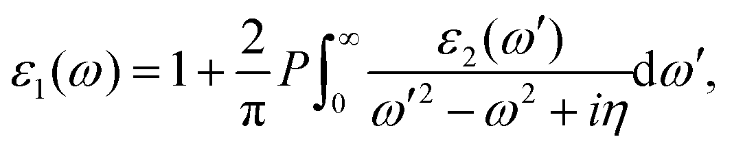
k point. And the real part of the dielectric matrix is determined by the Kramers–Kronig transformation:
| |  | (2) |
where
P is the principal value of the integral.
Then the main optical spectra, including the absorption coefficient I(ω), electron energy-loss spectrum L(ω), reflectivity R(ω), refractive index η(ω), and extinction coefficient K(ω), can be obtained from the dynamical dielectric response functions ε(ω). The specific expressions are given by:
| |  | (3) |
| | | L(ω) = ω2/[ε1(ω)2 + ε2(ω)2], | (4) |
| |  | (5) |
| |  | (6) |
and
| |  | (7) |
respectively.
3 Results and discussion
3.1 Geometry of the Janus MoSeTe monolayer
The crystal structures of the Janus MoSeTe monolayer are shown in Fig. 1(a and b) with 2H and 1T phases, respectively. Similar to parental MoSe2, MoTe2 and other transition-metal dichalcogenides (TMDs), the Janus MoSeTe monolayer has a graphene-like honeycomb lattice,40 where the metal Mo layer is sandwiched with two different kinds of chalcogen atoms, i.e., Se and Te atoms, with the sequence of Se–Mo–Te. Depending on the arrangement of chalcogen atoms, the traditional TMDs structure appears in two district symmetries: the 2H (trigonal prismatic D3h) phase and the 1T (octahedral) phase. The 2H phase shows a hexagonal lattice with a threefold-symmetry. The Se–Mo/Te–Mo atoms are in an eclipsing geometry from the top view, and hence the atomic stacking sequence is AB, as shown in Fig. S1(a and b) for MoSe2 and MoTe2, respectively (ESI†). However, the 1T structure has an ABC stacking sequence in which the top Se/Te atoms occupy the hollow center of the 2H hexagonal lattice, as shown in Fig. S2 (ESI†). Intriguingly, one of the unique properties of the MoSeTe monolayer is the Janus asymmetry where the structural imbalance in the MoSeTe monolayer breaks the traditional reflection symmetry along the out-of-plane direction, resulting in a spontaneous electric field within the monolayer. Also it is worth noting that the symmetry of Janus MoSeTe in the 2H phase is lower than those of the MoSe2 and MoTe2 monolayers though their structures are similar.
 |
| | Fig. 1 Top (upper) and side (bottom) views of 2D Janus MoSeTe in (a) 2H and (b) 1T phases, respectively. The purple, dark yellow, and green spheres represent Mo, Te and Se atoms, respectively. | |
For the newly proposed 2D materials, we first calculated the phonon dispersions of the Janus MoSeTe monolayer to confirm their structural stability. Our calculations show that there are no imaginary frequencies in the phonon dispersions of the Janus MoSeTe monolayers in both 2H and 1T phases, indicating that they are dynamically stable, as depicted in Fig. S3 (ESI†). But the total energy calculations show that the 2H phase is lower than the 1T phase by 0.113 eV per unit, as shown in Fig. S4 (ESI†). The calculated geometry and the lattice parameters of the optimized Janus MoSeTe are shown in Table 1. The obtained lattice parameters of the 2H phase, i.e., 3.405 Å, is in agreement with the previous values of 3.394 Å41 and 3.43 Å.42 Besides, the in-sheet lattice constant of 2H-MoSeTe is only 0.06 Å longer than that of the 1T-MoSeTe monolayer. In addition, we determine the thicknesses of the 2H and 1T MoSeTe monolayers to be 3.491 Å and 3.623 Å, respectively. And the lengths of the Mo–Se (Mo–Te) bond are 2.548 Å (2.713 Å) and 2.537 Å (2.764 Å) with respect to 2H and 1T phases, respectively. Accordingly, their formation energies Efor are calculated by Efor = E(MoSeTe) − NMoE(Mo) − NSeE(Se) − NTeE(Te), where E(MoSeTe), E(Mo), E(Se), and E(Te) are the energies of the MoSeTe monolayer, Mo, Se, and Te stable bulks, respectively. N denotes the total number of specific atoms in a unit cell. Our calculations show that the 2H-MoSeTe monolayer is energetically more favorable with −1.945 eV in energy lower than −0.795 eV for the 1T-MoSeTe monolayer, which is in agreement with the results of the total energy in Fig. S4 (ESI†).
Table 1 Calculation of the lattice constants, Mo–Se and Mo–Te bond lengths, thickness, formation energies and band gap of Janus MoSeTe in 2H and 1T phases, respectively
|
|
a (Å) |
d
Mo–Se (Å) |
d
Mo–Te (Å) |
h (Å) |
E
for (eV per atom) |
E
PBEg (eV) |
E
PBE+SOCg (eV) |
E
HSEg (eV) |
E
HSE+SOCg (eV) |
| 2H-MoSeTe |
3.405 |
2.548 |
2.713 |
3.491 |
−1.945 |
1.336 |
1.225 |
1.859 |
1.726 |
| 1T-MoSeTe |
3.345 |
2.537 |
2.764 |
3.623 |
−0.795 |
0.182 |
0.076 |
0.319 |
0.202 |
3.2 Electronic structures of the Janus MoSeTe monolayer
A precise evaluation of the electronic structure of Janus MoSeTe is indispensable in which the optical spectra are directly calculated from the interband transitions. Thus, the band structures of Janus MoSeTe along the highly symmetric M–Γ–K–M path in the Brillouin zone are calculated by the HSE06, HSE + SOC, PBE and PBE + SOC functionals and the results are shown in Fig. 2, Fig. S5 and S6 (ESI†), respectively. Apparently, there are certain differences in the band structures of the 2H and 1T phases. In the case of the 2H-MoSeTe monolayer in Fig. 2(a), we can find that it is a semiconductor with a direct band gap of 1.859 eV, which suggests that the 2H structure of Janus MoSeTe would be an excellent light harvesting 2D material. The HSE + SOC value is 1.726 eV, which is consistent with the previous value of 1.70 eV.42 The corresponding band gaps with PBE and PBE + SOC are 1.336 eV and 1.225 eV for the 2H structure, which are comparable with the previous results of 1.34 eV and 1.22 eV using GGA and GGA + SOC, respectively.41 It is worth noting that the gap of Janus MoSeTe in the 2H phase is in between the results of MoS2 and MoTe2.43 The band gaps of the 1T phase are 0.319 eV and 0.202 eV with respect to HSE and HSE + SOC functions. The corresponding PBE and PBE + SOC results are 0.182 eV and 0.076 eV, respectively. The details are listed in Table 1. We can see that SOC has little effects on the band gaps of the pristine MoSeTe structure. Remarkably, the top valence bands at the K point are always higher than those at the Γ point for the 2H phase, and the energy differences are respectively 274 meV and 197 meV as determined using HSE and PBE calculations, larger than the thermal energy at room temperature (KT ∼ 25.8 meV), indicating that the electrons could be directly photoexcited from the valence band to the conduction band, which is feasible for the generation of photogenerated electrons and holes. Different from the case of the 2H structure, the maximum of the valence band and the minimum of the conduction band occur at the K point and along the Γ–K direction to the 1T-MoSeTe monolayer, respectively, resulting in an indirect-gap behavior. Besides, the band gap of the 1T phase is smaller with a value of 0.3191 eV at the HSE level, implying that 1T-MoSeTe is not an optically transparent material in which there will be amount of carriers created by absorption of light at room temperature.
 |
| | Fig. 2 Band structure of the Janus MoSeTe monolayer in (a) 2H and (b) 1T phases, respectively, obtained using the hybrid functional HSE06. The dotted lines indicate the position of the Fermi level. | |
In order to further elucidate the electronic properties of the Janus MoSeTe monolayer, the total density of states and the projected density of states for Mo 4d, Te 5p and Se 4p are calculated using the HSE functional, as depicted in Fig. 3. It is clearly shown that the valence bands are mainly contributed by Mo 4d orbitals with a little Te 5p and Se 4p contribution in both 2H and 1T phases. The Mo 4d valence band covers from −6 to 0 eV for the 2H phase and −7 to 0 eV for the 1T phase, respectively. Moreover, hybridization between Mo 4d and Te 5p orbitals is larger than Mo 4d and Se 4p orbitals under the Fermi level in both 2H and 1T structures since the bandwidth of the valence bands for the Te atom is relatively larger than that of the Se atom. Regarding the unoccupied Mo 4d orbitals, an accurate description is also necessary for the interband transitions since electrons are generated from the occupied valence bands to the unoccupied conduction bands during optical excitations. For the 2H-MoSeTe monolayer, the Mo 5d, Te 5p and Se 4p bands originate at about 1.84 eV, 1.82 eV, and 1.78 eV, respectively. In contrast, the bands of the 1T phase above the Fermi level originate at larger than 0.391 eV, as shown in Fig. 3(d, f and h) with respect to Mo, Te, and Se atoms, resulting in a smaller band gap. These results imply that the band gap is very sensitive to the arrangement of atoms along the in-plane direction and could be modulated by varying the interatomic separations and angles.
 |
| | Fig. 3 Total DOS and projected density of states (PDOS) of the Janus MoSeTe monolayer in the 2H phase (left) and the 1T phase (right), obtained using the hybrid functional HSE06. The dotted lines indicate the position of the Fermi level. | |
4 Optical properties of the Janus MoSeTe monolayer
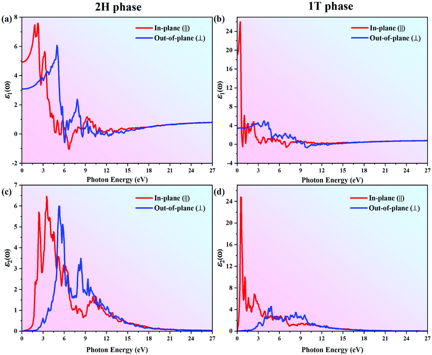
In this section, we discuss the optical response of the Janus MoSeTe monolayer. The calculated dynamical dielectric functions using the HSE functional of the MoSeTe monolayer, including the imaginary part ε2(ω) and real part ε1(ω) of the dielectric function ε(ω) are displayed in Fig. 4 with respect to 2H and 1T phases, whereas the optical spectra using the PBE functional is depicted in Fig. S7 (ESI†). On the basis of structural anisotropy, the corresponding ε(ω) is split into three parts: xx, yy and zz directions with εxx = εyy ≠ εzz, so we can see different behaviours when the incident photons are polarized the in-plane and out-of-plane of the 2H-/1T-MoSeTe monolayer. The main difference between these spectra is that ε(ω)‖ is more intense in the low range of 0–3.5 eV, whereas ε(ω)⊥ is more intense in the high range of energy (4–11 eV) based on the observed blue shift for the threshold peaks of ε(ω)⊥.
 |
| | Fig. 4 The dynamical dielectric function ε(ω) = ε1(ω) + ε2(ω) as a function of the photon energy for the Janus MoSeTe monolayer in the 2H phase (left) and the 1T phase (right) obtained using the hybrid functional HSE06. | |
The calculated static optical dielectric constants (ε∝) in-plane are 4.939 and 19.359 for 2H and 1T phases, respectively, which turn to be 3.082 and 3.456 out-of-plane, indicating that 1T-MoSeTe has a relatively high polarizability. Besides, the negative values occur from 5.96 eV to 7.36 eV for the 2H phase, whereas they emerge at around 9.16 eV and 10.00 eV to the 1T phase, as shown in Fig. 4(a and b) respectively, which unveils the metallic feature of the 2H and 1T phases in the ultraviolet part of the electromagnetic spectrum.44
Regarding the imaginary part ε2(ω), the first peak locates at 1.928 eV (0.480 eV), similar to the band gap of 1.859 eV (0.391 eV) of the 2H (1T) MoSeTe construction, indicating that photoexcited electrons can directly transit from the VBM to the CBM. The second and third peaks locate at 2.337 eV and 3.272 eV for the 2H phase, respectively. The photon energy of the visible light ranges from 1.63 to 3.12 eV, suggesting that the 2H-MoSeTe monolayer is a good light harvesting material. Besides, this visual light absorption is mainly contributed by the in-plane εxx2 and εyy2 components. It is noticed that there are several peaks for the out-of-plane εzz2 of the 2H phase: at 2.92 eV, 3.74 eV, 5.32 eV, 8.36 eV, and 9.35 eV, showing that the εzz2 cannot be neglected in the ultraviolet range. However, for the 1T phase, the second peak occurs at 0.960 eV. According to our calculated PDOS in Fig. 3(d), we suggest that this peak is assigned to the intra Mo 5d transitions. Similarly, the εzz2 component of the 1T phase makes an essential contribution between 2.72 eV and 10.50 eV, which can be due to the electronic transitions from the 5d states to the hybridized 5d/4p or 5d/5p orbitals.
On the other hand, the e–e correlation is considered to be the imaginary part ε2(ω) of the dielectric function for Janus MoSeTe by using G0W0 functions. Moreover, the G0W0 plus Bethe–Salpeter equation (BSE) which introduces higher order interaction diagrams, i.e., e–e and e–h effects, is also considered to improve the electronic description systematically on top of G0W0.45,46 The obtained results are shown in Fig. S8 (ESI†). It is clear that the optical anisotropy between εxx2 (or εyy2) and εzz2 largely increases by the inclusion of local field effects, as shown in Fig. S8(a) vs. (c) or Fig. S8(b) vs. (d) (ESI†). Additionally, the e–h interaction produces mainly a renormalization of the intensity of the optical peaks calculated using the HSE + G0W0 + BSE function. More inspecting the imaginary part of the dielectric functions obtained at the HSE and G0W0 levels for both phases, one can see that the inclusion of the e–e interaction leads to a blue shift. However, the inclusion of both e–e and e–h interactions yields a significant red shift, which is in agreement with the previous results.47–49 Another appealing peculiar result is that the first BSE optical peak is in much better agreement with the electronic gap than the other two calculated results, implying the weakly bound excitonic/free carrier nature of the optical excitation. Thus, the physical effect of the e–e and e–h interactions, reproduced by the HSE + G0W0 + BSE function, provides a more precise result. However, the total computation by HSE + G0W0 + BSE is much more expensive than other methods. More importantly, it is worth mentioning that the global shape of the spectrum is preserved and calculated by these three methods for both 2H and 1T phases of the MoSeTe monolayer. Considering the above factors, the optical properties of Janus MoSeTe could be well explained by independent-particle transitions.
Fig. 5 shows the relationships of the adsorption coefficient I(ω), energy-loss L(ω) and the reflectivity R(ω) with photon energy for the Janus MoSeTe monolayer in the HSE functional obtained from the relation (eqn (3)-(5)) (see Fig. S9 for the comparison of PBE results, ESI†). For the absorption coefficient I(ω) spectrum, which describes the decay of light traveling through the unit distance in an absorbing medium, there are many peaks within the studied energy range. The obtained I(ω) is zero when the photon energy is below 1.57 eV and 0.35 eV for 2H and 1T phases, respectively. Correspondingly, it is located at 3.09 eV and 1.22 eV for MoSe2 and MoTe2 monolayers in the 2H phase, as shown in Fig. S13(a and b), respectively (ESI†). From the MoSe2 to MoSeTe to MoTe2 monolayer in the 2H phase, we find that the red shift becomes stronger. This change is in good agreement with the trend of the band gap variance in which the minimum photon energy required for the electron interband transitions must be larger than the band gap. Thereafter, the adsorption coefficient gradually increases, implying that the absorption processes occur at the corresponding photon energies. Notably, the absorption coefficient could also describe the attenuation of intensity, i.e., the absorption spectra have a relatively low intensity with a small energy area since there are few electronic states that could play a role as the initial state in the absorption processes. Furthermore, the maximum peak of I(ω) could reach up to 1 × 10⁶ at 8.53 eV and 9.71 eV for Janus MoSeTe in 2H and 1T phases, respectively, implying high efficiency in the utilization of solar energy. Compared with the absorption coefficients (<1 × 10⁶) of MoS250 and MoSSe,51 we found that the obtained values are slightly larger than those of TMD materials. Besides, the obtained results are comparable to the values of MoSe2 and MoTe2, as shown in Fig. S13 (ESI†). Additionally, the rest of the peaks occur at 2.69, 4.67, 9.35, 10.75 eV for the 2H phase, and 0.59, 3.18, 6.88, 12.76 eV for the 1T phase. These results show the same trend as that of the peaks of the imaginary part ε2(ω) discussed above, confirming that the Janus MoSeTe monolayer mainly absorbs the visible and ultraviolet part of the electromagnetic spectrum.
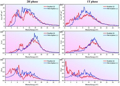 |
| | Fig. 5 Calculated absorption coefficient I(ω), the energy loss spectrum L(ω) and reflectivity R(ω) of the Janus MoSeTe monolayer in the 2H phase (left) and the 1T phase (right) obtained using the hybrid functional HSE06. | |
Electrons in a medium can get excited by absorbing photons carrying energy. On the other hand, a fast traveling electron in a solid medium will release some energy, which may excite other electrons in the material. Besides, not only single particle excitations but also collective excitations occur, which can be identified by analyzing the energy-loss L(ω) spectrum related to the dielectric function using eqn (4). In the case of intra- and interband transitions, L(ω) can demonstrate the plasmon excitations. The highest peak in the L(ω) spectrum indicates the characteristic associated with the plasma resonance and the corresponding highest frequency is the plasma frequency at which electrons could respond to.44,52 Thus, when electromagnetic waves have a lower frequency than the plasma frequency for the Janus MoSeTe monolayer, then the plasma oscillations will successfully screen the electric field since the electron has enough time to respond to the incident wave. As a result, the incident electromagnetic radiations are reflected from the surface of the Janus MoSeTe monolayer along with an increase in the reflection intensity. Hence, the peaks of L(ω) indicate the trailing edges in the reflection spectra.52 The maximum peak locates at 14.50 eV and 14.97 eV associated with 2H and 1T phases, as shown in Fig. 5(c and d), respectively, indicating the plasmon resonance. Similarly, these peaks correspond to the abrupt reduction of the absorption coefficient I(ω) and reflectivity R(ω) in Fig. 5(e and f), respectively. Additionally, the origin of these peaks can also be explained according to the structure displayed in the real part of the dielectric function. As shown in Fig. 4(a and b), the real part ε1 becomes zero at around 5.96 eV (7.10 eV), arriving the minimum at about 6.72 eV (9.94 eV), and again reaches zero at 14.97 eV (13.43 eV) for the 2H (1T) phase. Regarding MoSe2 and MoTe2, from Fig. S13(c and d) (ESI†), the highest peaks are located at 13.62 eV and 15.40 eV, respectively, showing a blue-shift from MoSe2 to MoSeTe to MoTe2. Notably, according to Schoenes's opinion, the energy where ε1 crosses the zero line with a positive slope is the plasmon excitation energy.53 Moreover, when the incident electromagnetic radiation with a larger frequency passes through the plasma, the plasma oscillation frequency cannot follow the oscillations with less time to respond in the electric field, and therefore, no considerable change occurs in the incident wave, resulting in the disappearance of reflectivity R(ω). Subsequently, the electromagnetic wave could enter and pass through the 2D MoSeTe monolayer with the energy loss which is described by the absorption coefficient I(ω) and the electronic energy loss spectrum L(ω).
In the reflectivity R(ω) curves in Fig. 5(e and f), there are many peaks up to 24 eV. The maximum reflectivity reaches 35% and 53% locating at 6.66 eV and 0.478 eV for the MoSeTe monolayer in 2H and 1T phases, respectively. Particularly, the reflectivity of the 1T phase is high in the IR region but decreases by about half to less than 30% in the visible and UV light regions, i.e., allowing UV and visible light to pass through the 1T-MoSeTe monolayer but reflecting the infrared radiation, resulting in limited heat levels with a minimum impact on the overall system performance. To the best of our knowledge, hot mirrors reflect IR radiation and transmit one or more non-IR irradiation. Therefore, the 1T-MoSeTe monolayer is a good hot mirror material that can be used as a thermal reflective coating in the fields of energy/conservation and environmental protection. In contrast, reflectivity is around 30% for MoSe2, MoSeTe and MoTe2 in the 2H phase in the whole spectral region, leading to mediocre optical properties.
Fig. 6 shows the relationships of the refractive index η(ω) and the extinction coefficient K(ω) with photon energy of the proposed materials. The static refractive indices of the 2H-MoSeTe monolayer are 2.22 and 1.76 and reach peak values of 2.83 and 2.55 with respect to the in-plane and out-of-plane direction as shown in Fig. 6(a). Thereafter, the refractive indices decrease steadily and tend to be constant in the far UV region. Correspondingly, the static refractive indices of the 1T phase are 4.484 and 1.861 for the in-plane and out-of-plane direction, respectively. But the difference of the peak values between them reaches up to 2.953, as clearly shown in Fig. 6(b). More obviously, η‖(ω) decreases dramatically in the IR region, and when the photon energy exceeds 16 eV, it tends to be constant. The static refractive indices of MoSe2 and MoTe2, by contrast, are in the range of 1.94–2.47, but the peak values are 3.12 (MoSe2), 3.25 (MoTe2), respectively, which are larger than that of 2H-MoSeTe. For the extinction coefficient K(ω), it can be seen that the basic nature is the same for the in-plane and out-of-plane direction of the 2H phase with a blue-shift of maximally 2.70 eV relative to the in-plane direction. A similar trend is also observed in MoSe2 and MoTe2 from Fig. S14 (ESI†). However, in the case of 1T-MoSeTe, an additional peak appears in the spectrum at 0.504 eV for the in-plane direction, and then the peak height drops sharply in the visible and ultraviolet region, which tends to be constant after 24 eV, as shown in Fig. 6(d). In broad terms, the large peak width of the extinction coefficient indicates that the photons could be absorbed quickly, since its depth path is the shortest. The penetration depth (δ = c/2πωK),54i.e., the skin depth, could correctly provide the penetration length at which the intensity of light or any electromagnetic radiation penetrating inside a material will fall to 1/e or 37% of its original value at the surface. From MoSe2 to MoSeTe to MoTe2 in the 2H phase, the calculated maximum depths are around 29 (22) nm, 25 (16) nm, and 24 (15) the in-plane (out-of-plane) direction, respectively. However, for the 1T-MoSeTe monolayer, it goes up to 117 nm (16 nm). Since the thickness of these 2D monolayers is less than 0.4 nm, the δ makes little sense.
 |
| | Fig. 6 Calculated refractive index n(ω) and extinction coefficient K(ω) for the Janus MoSeTe monolayer in the 2H phase (left) and the 1T phase (right) obtained using the hybrid functional HSE06. | |
The absorbance A(ω) of the Janus MoSeTe monolayer is calculated according to the Taylor expansion for a small thickness Δz → 0,55,56
Correspondingly, transparency
T(
ω) can be derived as,
| | | T(ω) = 1 − R(ω) − A(ω). | (9) |
The calculated results are shown in
Fig. 7. One can see that there are many peaks at about 2.54, 4.65, 6.76, 8.46 and 12.36 eV in the absorbance spectrum. The high absorbance
A(
ω) spectrum is about 2% in the visible range for both 2H and 1T phases, which is comparable with the measured value of 2.8% for black phosphorus.
57 Also one can see from Fig. S15 (ESI
†) that the integrated absorbance of the parental MoSe
2 and MoTe
2 is calculated to be a multiple of 3.55% and 4.44%, which are larger than that of the Janus MoSeTe monolayer. In addition, the sharp absorbance peaks are observed around 8–9 eV with 3.63% and 4.83% for 2H and 1T MoSeTe, respectively. It is deduced that the MoSeTe monolayer can capture a significant fraction of sunlight in a subnanometer thickness. Additionally, it is observed that the overall absorbance magnitude is lower for the 2H phase than that of the 1T phase. In contrast, the overall transmittance magnitude is higher for the Janus MoSeTe monolayer. In the ranges of 0–3.08 eV, 8–10 eV and 14–27 eV, the 2H MoSeTe monolayer is observed to transmit almost 90% of the incident light. Thus, we can predict that green, blue, violet and ultra-violet light are least absorbed,
i.e., the most transmitted and absorbed in the Janus MoSeTe monolayer, indicating that the MoSeTe monolayer would be most easily seen with a green, blue, and violet filter. Furthermore, it is observed that the MoSeTe monolayer generally transmits more red light than violet light. For comparison, the average optical transmittance in the region of 0.88–2.78 eV is less than 80% for MoSe
2, suggesting that it transmits more red, orange, yellow and green light, which is similar to MoTe
2 in Fig. S15(d) (ESI
†).
 |
| | Fig. 7 Calculated absorbance and transmission spectrum for the Janus MoSeTe monolayer in the 2H phase (left) and the 1T phase (right) obtained using the hybrid functional HSE06. | |
We also studied the optical properties of Janus MoSeTe monolayer that sunlight goes through the 25 opposite orientation due to the structural anisotropy. Surprisingly, the shapes of the calculated optical spectra for different orientations exhibit almost the same main features. This might be because the slight difference in the optical thicknesses between dMo–Se and dMo–Te for the MoSeTe monolayer results in a similar interaction between light with surface Se and Te atoms, which could be used in strengthening light reflection or transmission, and spectra splitting. In order to meet the higher requirements for optical characteristics, stacking systems should be used in which it can broaden the spectral range or bring about new functionalities, like polarizers. On the other hand, the greater intensities of light due to the multilayer coating could produce nonlinear effects, and accounting for these will certainly require further research.28
5 Conclusions
We have performed a comprehensive investigation of the electronic and optical properties of the Janus MoSeTe monolayer in 2H and 1T phases, with a detailed comparison of the parental MoSe2 and MoTe2 monolayer, through first-principles calculations based on DFT. Firstly, our calculations show that Janus MoSeTe in 2H and 1T structures exhibit dynamical stability and high experimental feasibility. Besides, we demonstrate that the 2H structure shows a direct bandgap of 1.859 eV and an indirect gap of 0.391 eV for the 1T structure, which triggers plasmons absorbing light at different frequencies. Besides, the SOC has little effects on the band gaps. Analytically, we obtain microscopic insights into the origins of the maximum optical response which shows a significant red shift from the MoSe2 to MoSeTe to MoTe2 monolayer. However, the blue-shift exists from the in-plane to out-of-plane direction. Compared with the HSE results, it is found that the inclusion of the e–e interaction led to a blue shift of ε2(ω). However, the inclusion of both e–e and e–h interactions results in a significant red shift. Phenomenologically, 1T-MoSeTe interacts with light strongly from the infrared to visible to ultraviolet regions due to its small band gap nature. More importantly, the maximum reflectivity of the 1T phase reaches up to 53% at 0.478 eV, enabling it to be a good hot mirror material. In addition, the absorption coefficient values could reach up to 1 × 106 cm−1 in both phases, implying the high efficiency in the utilization of solar energy of the MoSeTe monolayer. Additionally, the average optical absorbance of the Janus MoSeTe monolayer in the visible light region is calculated to be 2% and the corresponding transmittance is around 80%. Furthermore, the optical response orientated to the opposite surface is also considered in our work due to the intrinsic asymmetric structure of Janus MoSeTe. Surprisingly, our results show a similar sensitivity to a particular wavelength of light in different optical ranges. Our findings not only predict the great potential application of Janus MoSeTe in ultra-thin reflectors and absorbers for optoelectronic devices, but also may provide guidelines to the discovery of new optical science and the realization of various light emission, detection, modulation, and manipulation functions in specific frequency ranges.
Conflicts of interest
There are no conflicts to declare.
Acknowledgements
We sincerely acknowledge the financial support from the National Natural Science Foundation of China (Grant No. 11705152, 11625415, and 41272050), the Joint Fund of the National Natural Science Foundation of China and the China Academy of Engineering Physics (Grant No. U1530258), the Science Challenge Project (Grant No. TZ2016001), the National Magnetic Confinement Fusion Energy Research Project of China (Grant No. 2015B108002), and the Longshan academic talent research supporting program of Southwest University of Science and Technology (Grant No. 18LZX513 and 18LZXT04). And the authors gratefully acknowledge financial support from the China Scholarship Council. DS and RA thank Carl Tryggers Stiftelse for Vetenskaplig Forskning (CTS) for financial support. SNIC and HPC2N are acknowledged for providing the computing facilities.
References
- S. Das Sarma, S. Adam, E. H. Hwang and E. Rossi, Rev. Mod. Phys., 2011, 83, 407–470 CrossRef CAS.
- K. S. Novoselov, A. K. Geim, S. V. Morozov, D. Jiang, Y. Zhang, S. V. Dubonos, I. V. Grigorieva and A. A. Firsov, Science, 2004, 306, 666–669 CrossRef CAS PubMed.
- R. R. Nair, P. Blake, A. N. Grigorenko, K. S. Novoselov, T. J. Booth, T. Stauber, N. M. Peres and A. K. Geim, Science, 2008, 320, 1308 CrossRef CAS PubMed.
- G. Eda and S. A. Maier, ACS Nano, 2013, 7, 5660–5665 CrossRef CAS PubMed.
- A. Splendiani, L. Sun, Y. Zhang, T. Li, J. Kim, C. Y. Chim, G. Galli and F. Wang, Nano Lett., 2010, 10, 1271–1275 CrossRef CAS PubMed.
- N. Alem, R. Erni, C. Kisielowski, M. D. Rossell, W. Gannett and A. Zettl, Phys. Rev. B: Condens. Matter Mater. Phys., 2009, 80, 155425 CrossRef.
- C. R. Dean, A. F. Young, I. Meric, C. Lee, L. Wang, S. Sorgenfrei, K. Watanabe, T. Taniguchi, P. Kim, K. L. Shepard and J. Hone, Nat. Nanotechnol., 2010, 5, 722–726 CrossRef CAS PubMed.
- H. Liu, A. T. Neal, Z. Zhu, Z. Luo, X. Xu, D. Tománek and P. D. Ye, ACS Nano, 2014, 8, 4033–4041 CrossRef CAS PubMed.
- M. Xu, T. Liang, M. Shi and H. Chen, Chem. Rev., 2013, 113, 3766–3798 CrossRef CAS PubMed.
- M. Chhowalla, H. S. Shin, G. Eda, L. J. Li, K. P. Loh and H. Zhang, Nat. Chem., 2013, 5, 263 CrossRef PubMed.
- J. N. Coleman, M. Lotya, A. O. Neill, S. D. Bergin, P. J. King, U. Khan, K. Young, A. Gaucher, S. De, R. J. Smith, I. V. Shvets, S. K. Arora, G. Stanton, H. Y. Kim, K. Lee, G. T. Kim, G. S. Duesberg, T. Hallam, J. J. Boland, J. J. Wang, J. F. Donegan, J. C. Grunlan, G. Moriary, A. Shmeliov, R. J. Nicholls, J. M. Perkins, E. M. Grieveson, D. W. McComb, K. Theuwissen, P. D. Nellist and V. Nicolosi, Science, 2011, 331, 568–571 CrossRef CAS PubMed.
- B. Anasori, M. R. Lukatskaya and Y. Gogotsi, Nat. Rev. Mater., 2017, 2, 16098 CrossRef CAS.
- L. Tao, E. Cinquanta, D. Chiappe, C. Grazianetti, M. Fanciulli, M. Dubey, A. Molle and D. Akinwande, Nat. Nanotechnol., 2015, 10, 227 CrossRef CAS PubMed.
- M. Dávila, L. Xian, S. Cahangirov, A. Rubio and G. Le Lay, New J. Phys., 2014, 16, 095002 CrossRef.
- S. Balendhran, S. Walia, H. Nili, S. Sriram and M. Bhaskaran, Small, 2015, 11, 640–652 CrossRef CAS PubMed.
- A. J. Mannix, X. F. Zhou, B. Kiraly, J. D. Wood, D. Alducin, B. D. Myers, X. Liu, B. L. Fisher, U. Santiago, J. R. Guest, M. J. Yacaman, A. Ponce, A. R. Oganov, M. C. Hersam and N. P. Guisinger, Science, 2015, 350, 1513–1516 CrossRef CAS PubMed.
- D. Singh, S. K. Gupta, Y. Sonvane and I. Lukačević, RSC Adv., 2016, 6, 8006–8014 RSC.
- X. H. Liu, C. Z. Guan, D. Wang and L. J. Wan, Adv. Mater., 2014, 26, 6912–6920 CrossRef CAS PubMed.
- L. Dou, A. B. Wong, Y. Yu, M. Lai, N. Kornienko, S. W. Eaton, A. Fu, C. G. Bischak, J. Ma, T. Ding, N. S. Ginsberg, L. W. Wang, A. P. Alivisatos and P. Yang, Science, 2015, 349, 1518–1521 CrossRef CAS PubMed.
- R. Ma and T. Sasaki, Adv. Mater., 2010, 22, 5082–5104 CrossRef CAS PubMed.
- R. Ma and T. Sasaki, Acc. Chem. Res., 2014, 48, 136–143 CrossRef PubMed.
- A. Y. Lu, H. Zhu, J. Xiao, C. P. Chuu, Y. Han, M. H. Chiu, C. C. Cheng, C. W. Yang, K. H. Wei, Y. Yang, Y. Wang, D. Sokaras, D. Nordlund, P. Yang, D. A. Muller, M. Y. Chou, X. Zhang and L. J. Li, Nat. Nanotechnol., 2017, 12, 744 CrossRef CAS PubMed.
- J. Zhang, S. Jia, I. Kholmanov, L. Dong, D. Er, W. Chen, H. Guo, Z. Jin, V. B. Shenoy and L. Shi,
et al.
, ACS Nano, 2017, 11, 8192–8198 CrossRef CAS PubMed.
- Q. F. Yao, J. Cai, W. Y. Tong, S. J. Gong, J. Q. Wang, X. Wan, C. G. Duan and J. Chu, Phys. Rev. B, 2017, 95, 165401 CrossRef.
- L. Dong, J. Lou and V. B. Shenoy, ACS Nano, 2017, 11, 8242–8248 CrossRef CAS PubMed.
- F. Li, W. Wei, H. Wang, B. Huang, Y. Dai and T. Jacob, J. Phys. Chem. Lett., 2019, 10, 559–565 CrossRef PubMed.
- X. Yuan, M. Yang, L. Wang and Y. Li, Phys. Chem. Chem. Phys., 2017, 19, 13846–13854 RSC.
- S. Gupta, S. N. Shirodkar, A. Kutana and B. I. Yakobson, ACS Nano, 2018, 12, 10880–10889 CrossRef CAS PubMed.
- B. Hammer, L. B. Hansen and J. K. Nørskov, Phys. Rev. B: Condens. Matter Mater. Phys., 1999, 59, 7413 CrossRef.
- G. Kresse and J. Furthmüller, Phys. Rev. B: Condens. Matter Mater. Phys., 1996, 54, 11169 CrossRef CAS PubMed.
- J. Perdew, K. Burke and M. Ernzerhof, Phys. Rev. Lett., 1996, 77, 3865–3868 CrossRef CAS.
- S. Grimme, J. Antony, S. Ehrlich and H. Krieg, J. Chem. Phys., 2010, 132, 154104 CrossRef.
- H. Monkshort and J. Pack, Phys. Rev. B: Solid State, 1976, 13, 5188–5192 CrossRef.
- J. Heyd, G. E. Scuseria and M. Ernzerhof, J. Chem. Phys., 2003, 118, 8207–8215 CrossRef CAS.
- J. P. Perdew, A. Ruzsinszky, G. I. Csonka, O. A. Vydrov, G. E. Scuseria, L. A. Constantin, X. Zhou and K. Burke, Phys. Rev. Lett., 2008, 100, 136406 CrossRef.
- N. Bickers, D. Scalapino and S. White, Phys. Rev. Lett., 1989, 62, 961 CrossRef PubMed.
- A. Togo, F. Oba and I. Tanaka, Phys. Rev. B: Condens. Matter Mater. Phys., 2008, 78, 134106 CrossRef.
- E. Sanville, S. D. Kenny, R. Smith and G. Henkelman, J. Comput. Chem., 2007, 28, 899–908 CrossRef CAS PubMed.
- M. Gajdoš, K. Hummer, G. Kresse, J. Furthmüller and F. Bechstedt, Phys. Rev. B: Condens. Matter Mater. Phys., 2006, 73, 045112 CrossRef.
- C. Ataca, M. Topsakal, E. Aktürk and S. Ciraci, J. Phys. Chem. C, 2012, 116, 8983–8999 CrossRef CAS.
- S. D. Guo and J. Dong, Semicond. Sci. Technol., 2018, 33, 085003 CrossRef.
- Y. Ji, M. Yang, H. Lin, T. Hou, L. Wang, Y. Li and S. T. Lee, J. Mater. Chem. C, 2018, 122, 3123–3129 CAS.
- S. D. Guo and J. L. Wang, Semicond. Sci. Technol., 2016, 31, 095011 CrossRef.
- D. Singh, S. K. Gupta, Y. Sonvane and I. Lukačević, J. Mater. Chem. C, 2016, 4, 6386 RSC.
- M. Rohlfing and S. G. Louie, Phys. Rev. Lett., 1998, 81, 2312 CrossRef CAS.
- G. Kresse and J. Furthmüller, Comput. Mater. Sci., 1996, 6, 15–50 CrossRef CAS.
- Z. Guan, S. Ni and S. Hu, J. Phys. Chem. C, 2018, 122, 6209–6216 CrossRef CAS.
- H. Jin, T. Wang, Z. R. Gong, C. Long and Y. Dai, Nanoscale, 2018, 10, 19310–19315 RSC.
- F. Karlicky and M. Otyepka, J. Chem. Theory Comput., 2013, 9, 4155–4164 CrossRef CAS PubMed.
- N. N. Hieu, V. V. Ilyasov, T. V. Vu, N. A. Poklonski, H. V. Phuc, L. T. Phuong, B. D. Hoi and C. V. Nguyen, Superlattices Microstruct., 2018, 115, 10–18 CrossRef CAS.
- X. Ma, X. Wu and Y. Wang, J. Mater. Chem. A, 2018, 6, 2295–2301 RSC.
-
F. Wooten, Optical properties of solids, Academic Press, 1973, vol. 41, pp. 939–940 Search PubMed.
- J. Schoenes, Phys. Rep., 1980, 63, 301–336 CrossRef.
-
D. B. Tanner, Optical effects in solids, Cambridge University Press, 2019 Search PubMed.
- M. Bernardi, M. Palummo and J. C. Grossman, Nano Lett., 2013, 13, 3664–3670 CrossRef CAS PubMed.
- L. Yang, J. Deslippe, C. H. Park, M. L. Cohen and S. G. Louie, Phys. Rev. Lett., 2009, 103, 186802 CrossRef PubMed.
- A. Castellanos Gomez, L. Vicarelli, E. Prada, J. O. Island, K. Narasimha-Acharya, S. I. Blanter, D. J. Groenendijk, M. Buscema, G. A. Steele, J. Alvarez, H. W. Zandbergen, J. J. Palacios and H. S. J. V. D. Zant, 2D Mater., 2014, 1, 025001 CrossRef.
Footnote |
| † Electronic supplementary information (ESI) available. See DOI: 10.1039/c9tc03936h |
|
| This journal is © The Royal Society of Chemistry 2019 |
Click here to see how this site uses Cookies. View our privacy policy here. 
 Open Access Article
 This Open Access Article is licensed under a Creative Commons Attribution-Non Commercial 3.0 Unported Licence
 ab,
Deobrat
Singh
ab,
Deobrat
Singh