
 Open Access Article
 This Open Access Article is licensed under a
 Creative Commons Attribution 3.0 Unported Licence
Flame assisted chemical vapour deposition NiO hole transport layers for mesoporous carbon perovskite cells†‡
Heather M.
Yates
 *a,
Simone M. P.
Meroni
b,
Dimitrios
Raptis
b,
John L.
Hodgkinson
a and
Trystan M.
Watson
b
*a,
Simone M. P.
Meroni
b,
Dimitrios
Raptis
b,
John L.
Hodgkinson
a and
Trystan M.
Watson
b
aMaterials and Physics Research Centre, University of Salford, Manchester, M5 4WT, UK. E-mail: H.M.Yates@salford.ac.uk
bSPECIFIC, Swansea University, Bay Campus, Fabian Way, Crymlyn Burrows, Swansea, SA1 8EN, Wales, UK
First published on 15th October 2019
Abstract
Flame assisted chemical vapour deposition was utilised to directly deposit polycrystalline mesoporous NiO to enhance charge transport within carbon perovskite solar cells (C-PSC). This versatile technique is highly suited for deposition of large area thin films along with the ability to use simple, stable aqueous salts. The combination of low cost methods of screen printing and FACVD to produce the C-PSC make this an attractive route towards commercialisation. The effects of deposition parameters on the morphology, crystallinity and density of the deposited NiO are discussed, along with the importance of use of a low propane, ‘lean flame’ on both the NiO and underlying F-doped tin oxide electrode. The thickness of the NiO layer was found to be critical in optimising the C-PSC efficiency. Addition of the NiO layer resulted in an increased short circuit current density (17.30 mA cm−2 to 20.28 mA cm−2). At an estimated NiO thickness of 17 nm the average cell efficiency (10.73%) surpassed that of the control sample (9.08%) so confirming the promise of this technique.
Introduction
Organic–inorganic lead halide perovskite solar cells are continuing to be considered as highly significant for solar cell performance. Although many issues such as stability and suitable large-scale manufacturing processes for the multilayer structure still need to be resolved. Efforts to remove these problems have led to a wide variety of different chemical components and cell configurations.1 One of the more stable structures has been shown to be a p–i–n mesoporous stack consisting of a top carbon electrode, insulating ZrO2 and bottom electron transfer layer (ETL) of TiO2.2On a conductive F-doped SnO2 (FTO) glass substrate with compact TiO2 sprayed on the top, porous layers of TiO2, ZrO2, and carbon are subsequently screen printed and fired to remove the organic binder. Finally, the perovskite precursor solution is infiltrated through the triple stack, in which porosity determines the crystallinity of the light harvesting material. This carbon perovskite solar cell architecture (C-PSC) is fully printable by a low-cost screen-printing process, free from expensive materials, such as noble metals (used as electrodes), Spiro OMeTAD (often used as the Hole Transport Layer, HTL), and with proven stability over one year under continuous illumination.3 The outstanding stability can be attributed to the 2D/3D perovskite of the CH3NH3PbI3 (Methylamine lead iodide, MAPI) with the addition of NH3(CH2)4COOHI (5-amino valeric acid iodide, AVAI).
The use of a cost effective transparent front electrode of FTO rather than indium tin oxide (ITO) with the issue of expensive and limited indium resources, and low-cost deposition methods makes the product more commercially attractive. Due to the low capital cost of the C-PSC, a step towards large scale deposition of these cells has been shown by various groups in both series and parallel connected modules,3,4 including that with the exceptional size of 198 cm2 active area.5 This latter was produced by a screen-printing technique. Other viable techniques for large area perovskite cells have also been reported such as slot-die,6,7 evaporation8 and ink-jet.9 Slot-die coating in particular provides a method which results in little materials wastage during coatings with the potential for high coating line speeds and roll-to-roll production for both rigid and flexible substrates.10,11
Previous studies12 have shown that adding an extra mesoporous layer of NiO as HTL improves the efficiency of charge extraction to the external circuit. The improvement from 8% to 15% for respectively devices without and with NiO interlayer, was then confirmed by Liu et al. with the use of a mixed cation perovskite composition.13
In this paper we utilise the properties of Flame Assisted Chemical Vapour Deposition (FACVD) in directly depositing porous NiO within the cell stack. FACVD has major advantages over many other techniques used to deposit coatings. Relatively simple engineering and the ability to run under atmospheric pressure gives reduced set-up and running costs. More importantly it is fully compatible with in-line commercial coating technologies with no restraint on sample size. Previously we have demonstrated that due to the energy provided by the flame the precursors can be readily available low cost aqueous salts, for deposition of thin films of silver,14 copper and silica oxides.15 These aqueous solutions greatly increase the ease of use and a reduction in environmental impact with the absence of organic precursors or solvents usually required for spin coating16 or Aerosol Assisted CVD (AACVD).17,18 In addition, FACVD films are polycrystalline and need no further processing, which is often a requirement when films are solution fabricated.
The application of the FACVD method on C-PSC's is also shown. Devices with a cell size of 1 cm2 were infiltrated with a solution of AVA-MAPI. We describe the optimisation of the mesoporous NiO layer in terms of thickness for the C-PSC.
Experimental
Deposition of NiO
A FACVD system, as previously described,19 was used to deposit the NiO films. A 0.05 M aqueous nickel nitrate solution was prepared from nickel nitrate hexahydrate (99.999% Sigma) and delivered as an aerosol via an ultrasonic nebuliser with a nitrogen carrier gas flow of 2 L min−1. The precursor, along with 0.6 L min−1 oxygen, was added to the combustion gases (0.8 to 1.0 L min−1 propane/22 to 20 L min−1 air) upstream of the burner head. The glass substrate was heated to 400 °C and translated at a rate of 10 mm s−1 under the flame to mimic an online process. The number of passes of the substrate under the flame was varied from 4 to 50. The substrate was either borosilicate glass or the initial solar cell structure of commercially available TEC720 with thin films of TiO2 and ZrO2, as described in the next section.Cell fabrication
For the C-PSC, on a FTO/glass substrate, layers of compact TiO2, mesoporous TiO2, ZrO2, and carbon were deposited as previously reported.21 The compact TiO2 was sprayed with a solution of Titanium diisopropoxide bis(acetylacetonate) (Sigma) in isopropanol 10% vol. The mesoporous TiO2, ZrO2 and carbon layers were screen printed with respectively 30NR-D (GreatcellSolar), ZT-SP (Solaronix) and GEM. The annealing of each layer occurred at 550 °C for TiO2, and 400 °C for ZrO2 and carbon. In the case of deposition of NiO in the architecture, the FACVD occurred on the ZrO2 layer before the deposition of the carbon. The perovskite solution was then infiltrated in the stack using a drop of solution of 439.0 mg, 151.4 mg, and 6.7 mg of respectively PbI2 (TCI), methylamine iodide (GreatcellSolar), and 5-aminovaleric acid iodide (GreatcellSolar) in 1 mL of γ-butyrolactone (Sigma). The wet devices were kept for 10 minutes at room temperature and then heated at 50 °C in oven. The devices were then placed in a humidity oven at 70% RH and 25 °C for 24 hours.Characterisation
Film morphology and thickness was obtained from scanning electron microscope images (FEI Quanta 250 ESEM) and subsequently analysed with ImageJ software for feature size.22 Atomic force microscopy (NanoScope IIIa, Digital Inst. Ltd) using Si tips in tapping mode surface was used to determine film roughness. X-ray diffraction (Siemens D5000) with a Cu Kα source was used for structural characterisation of the films. The scans were run over the 2θ range 20–60° using 8 s per step at 0.04 increments. Crystallite size was calculated from the Scherrer equation.23X-ray photoelectron spectroscopy (XPS) was performed on a Thermo Fisher Scientific NEXSA spectrometer. Samples were analysed using a micro-focused monochromatic Al X-ray source (72 W) over an area of approximately 400 microns. Data was recorded at pass energies of 200 eV for survey scans and 50 eV for high resolution scan with 1 eV and 0.1 eV step sizes respectively. Charge neutralisation of the sample was achieved using a combination of both low energy electrons and argon ions. Data analysis was performed in CasaXPS using a Shirley type background and Scofield cross sections, with an energy dependence of −0.6. The scans were calibrated using the C 1s binding energy of 285 eV.
The resistivity of the FTO substrates was measured using a Jandel Universal four point probe. Voltage–current characteristics were carried out using a Keithley 2400 source meter with a scan rate of 200 mV s−1 between −0.2 V and 1.1 V in dark and under illumination, in forward and reverse directions after 3 minutes of light soaking. A Newport Oriel solar simulator (class AAA) was used to simulate AM 1.5 solar spectrum. The calibration was with a KG5 filtered silicon reference cell. The printed cell size was 1 cm2, but to make sure the area was accurately defined an aperture mask with an area of 7 mm × 7 mm was used.
Results and discussion
Effects of FACVD deposition parameters
Inspection of the surface morphology by SEM established deposition by FACVD is via island growth. The thin film NiO initially deposits as small islands, which eventually coalesce and then start to thicken as films. Example SEM images (Fig. 1) show the film morphology, moving from individual islands to complete films. The films are not densely packed, although EDAX confirmed that all the particles (both large and small) for 50 passes are NiO.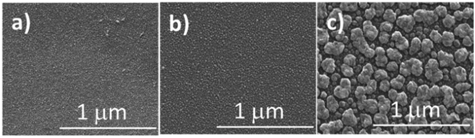 | ||
Fig. 1 SEM images of NiO on glass deposited via FACVD under a 1![[thin space (1/6-em)]](https://www.rsc.org/images/entities/char_2009.gif) :20 L min−1 propane:air flame. (a) 4 passes, (b) 10 passes, (c) 50 passes. :20 L min−1 propane:air flame. (a) 4 passes, (b) 10 passes, (c) 50 passes. | ||
The graph in Fig. 2 shows that for 10 or less passes of the substrate under the coater head there was limited change in film thickness, before becoming an approximately linear relationship. This is due to the island growth nature of the deposition process so initially the ‘thickness’ relates more accurately to the height of the individual islands of NiO. With increasing passes there is a gradual increase in coverage of the substrate, so the islands eventually coalesce and the thickness now relates to the film. Parallel with this is a gradual increase in film roughness (RMS) from 1 nm to 14 nm, mirroring the increasing number and size of the NiO islands. The latter increasing from 17 nm (σ = 5 nm) to 180 nm (σ = 50 nm) for 4 to 50 passes respectively. Calculations based on the linear part of the thickness curve (10 to 50 passes) gave a dynamic deposition rate of 1.12 nm per pass, which equates to a static deposition rate of 35 nm min−1. This is obtained from the pass rate and flame residence time. This will be the minimum deposition rate as if film continuity occurs not at 10 passes but at a greater number of passes the deposition rate would be increased. The majority of NiO thin films used for solar cells have been deposited by spin coating24–27 or by vacuum processes such as magnetron sputtering28,29 or atomic layer deposition (ALD). The former process is not suitable for large scale deposition and the latter are less flexible with slow growth processes and added complexity. For example Seo et al.30 reported an ALD deposition rate of 0.34 nm per cycle for NiO. However, the FACVD deposition rate is comparable to that reported by Sialvi et al.31 for AACVD of 18 nm min−1 to 31 nm min−1 for much thicker films (>500 nm). The deposition rates in Sialvi's paper were calculated from films deposited on TEC C15 (NSG) under the same conditions apart from deposition time and seems to have a non-linear relationship. This could be due to either mechanistic changes or non-uniform delivery of the precursor. This was a batch type reaction using nickel acetylacetonate in toluene.
 | ||
Fig. 2 Effect of number of passes with film thickness  and roughness, and roughness,  for FACVD NiO. for FACVD NiO. | ||
Furthermore, quantitative analysis of the SEM images confirmed the gradual increase in particle height variation as shown in the surface profile histogram in Fig. 3. The broadening of the peak half width as the number of passes of NiO increased relates to the widening range of feature sizes. In addition, at 10 passes and particularly distinctly for above 20 passes the histogram shows the presence of two distinct sets of features, at approximately the nominal values of 60 and 120. A higher x-axis value implies larger particle sizes.
 | ||
| Fig. 3 Height histogram obtained from surface images for various NiO films. | ||
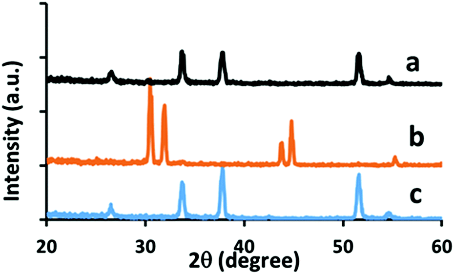
The films deposited were confirmed to be polycrystalline cubic NiO (space group Fm3m) with diffraction at 37° (111) and 43° (200) (JCPDS-47-1049). Two factors were found to improve the NiO crystallinity. Firstly, as previously reported by us, addition of oxygen to the precursors.32 Secondly, the proportion of propane/air within the flame. Reducing the amount of propane (1.0 L min−1 to 0.8 L min−1) and increasing the proportion of air (20 L min−1 to 22 L min−1) led to a slightly less reducing ‘lean’ flame and an improvement in crystallinity along with a change in orientation preference from (200) to (111). In Fig. 4 the XRD compares the crystallinity of two films of similar thickness (36 nm) deposited under standard (20 pass) and lean (50 pass) flame conditions. The 50 pass film deposited under standard flame conditions, although thicker is of lower crystallinity, as judged by its lower intensity and increased peak broadness. The modified flame conditions also showed an increase in crystallite size (7 ± 2 nm to 14 ± 1 nm) related to the less reductive flame.
 | ||
| Fig. 4 XRD of NiO films on glass. (a) 50 passes under lean flame, (b) 20 passes under standard flame, (c) 50 passes under standard flame. | ||
The lean flame gave a slower deposition rate, but a more compact film, for similar thickness as shown in Fig. 5, for a 36 nm thick NiO film. Measurements confirmed a reduction in particle size from 58 nm (σ = 14 nm) to 43 nm (σ = 9 nm) and a corresponding reduction in particle separation from 16 nm (σ = 11 nm) to 4 nm (σ = 1 nm) in changing to a lean flame.
 | ||
| Fig. 5 SEM images comparing two NiO films of similar thickness under different flame conditions. Insert shows cross-sections, (a) lean flame, (b) standard flame. | ||
A closer look at the surface chemistry and stoichiometry by X-ray Photoelectron Spectroscopy (XPS) confirmed the deposition of NiO, which under the less reducing lean flame was more stoichiometric NiO1.1 rather than that under the standard flame of NiO0.8. In both cases the Ni 2p showed a very similar structure with 2p3/2 at 854.1 eV with a spin orbital splitting Δ = 18.1 eV. This is slightly larger than the reference value of 17.5 eV,33 due to the difficulty in accurately determining the position because of the broad nature of the 2p peaks. However, our value is in line with that reported by other researchers.34,35 The high resolution scan showed six distinct peaks related to Ni 2p3/2 photoemission (Fig. 6). The assignments as shown in Table 1 are in agreement with Marrani et al.36 No peak relating to nickel metal (852.6 eV) was seen.
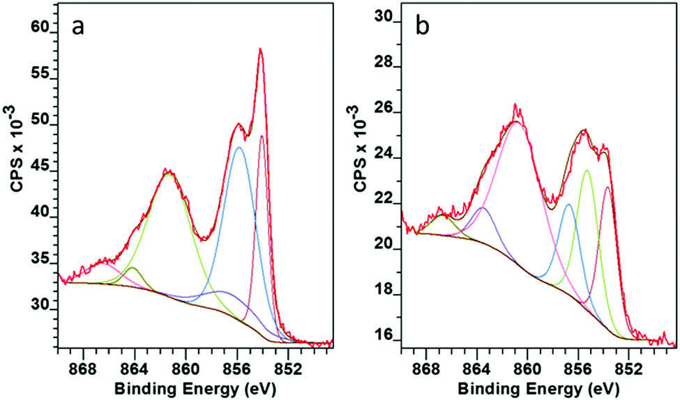 | ||
| Fig. 6 XPS Ni 2p3/2 spectra for NiO on glass deposited with (a) lean flame NiO, (b) standard flame (high propane). | ||
| Lean flame | |
|---|---|
| BE (eV) | Final state configuration |
| 854.1 | ![[c with combining low line]](https://www.rsc.org/images/entities/char_0063_0332.gif) d9 d9![[L with combining low line]](https://www.rsc.org/images/entities/char_004c_0332.gif) |
| 855.8 | d8:d9 |
| 856.4 | d9:d7 |
| 861.6 | d102 |
| 864.1 | d8 |
| 866.5 | Shake-up |
Within the complex 2p3/2 Ni structure the peaks round 854 eV and 855 eV have often been assigned to the Ni2+ and Ni3+ oxidation states respectively.37,38 Fitting of these two peaks confirmed that the change from a standard to a lean flame (more air, less propane) increased the amount of Ni3+ relative to Ni2+ from 0.78 to 1.05 (Ni3+/Ni2+). This is in line with the change to a less reducing flame. Stoichiometric NiO has a low intrinsic conductivity and self doping via Ni3+ acceptors into the lattice has been reported to make the material more conductive.39 This gave an extra incentive to use the lean flame to provide a more efficient HTL for C-PSC's.
The O 1s scan (Fig. S1, ESI‡) confirmed the assignment of NiO with a signal at 529.3 eV. For films deposited under a standard flame the strongest peak at 531.4 eV relates to absorbed hydroxyl peaks from water40 and a secondary resolved peak at 533.4 eV, which was assigned to C–O bonds.41 While for the lean flame sample these peaks are very much smaller than the metal related signal. It is possible that the greater porosity and hence surface area of the standard flame derived film led to increased amount of chemisorbed water over that of the more compact lean flame film. The strongest C 1s peak is the adventitious signal at 285 eV and as standard practice used for calibration. The lean flame showed two small resolved peaks at 286.6 eV and 288.7 eV assigned to C–OH and a π bonded C species42 such as C–C![[double bond, length as m-dash]](https://www.rsc.org/images/entities/char_e001.gif) O respectively (Fig. S1, ESI‡). These peaks are stronger under the standard flame, although on etching the intensities of the adventitious and C–CO drop so suggest they relate to surface contamination. The increase in the C–OH signal, along with the high O 1s –OH signal for the standard flame samples confirmed the higher presence of carbon related species in these films than those produced with the lean flame.
O respectively (Fig. S1, ESI‡). These peaks are stronger under the standard flame, although on etching the intensities of the adventitious and C–CO drop so suggest they relate to surface contamination. The increase in the C–OH signal, along with the high O 1s –OH signal for the standard flame samples confirmed the higher presence of carbon related species in these films than those produced with the lean flame.
The increased compactness of the film and reduction in pin-holes to the glass substrate was also apparent from the lack of any Si 2p signal in the survey scan for the lean flame film, while that from a similar thickness, less compact standard flame sample showed a small Si 2p signal at 103.2 eV usually assigned to silica.
It is important that the NiO film can be deposited without damage to the underlying layers. In this case the FTO front electrode and mesoporous TiO and ZrO2 layers. Checks on the effect of the flame on the FTO substrate showed the importance of using a lean flame. Under 50 passes of the standard flame FTO was reduced to tin metal (as confirmed by XRD, Fig. 7), along with very high sheet resistance. Under a lean flame (50 passes) there was no change to FTO in morphology, X-ray orientation, crystallite size, sheet resistance (7.4, σ = 0.5 Ω sq−1 to 7.1, σ = 0.2 Ω sq−1 (post flame)) or optical properties.
 | ||
| Fig. 7 XRD comparison on effects of flame on TEC 7 substrate. (a) 50 passes under a lean flame, (b) 50 passes under a standard flame, (c) as provided. | ||
Similarly tests on the subsequent TiO2 or ZrO2 layers showed no change in morphology or crystallographic orientation for any of the constituent layers. Both TiO2 (anatase, JCPDS 21-1272) and monoclinic ZrO2 (JCPDS 36-0420) were highly polycrystalline. Without the addition of NiO and a high number of passes under the flame (50) there was a small increase in crystallite size for TiO2 and ZrO2 (Table 2).
| Crystallite size, nm | TiO2 | FTO/ZrO2 |
|---|---|---|
| (101) 25.2° | (![[1 with combining macron]](https://www.rsc.org/images/entities/char_0031_0304.gif) 11) 28.1° 11) 28.1° |
|
| As provided | 15 | 16 |
| 50 pass flame | 17 | 18 |
| C-cell with 50 pass NiO | Not seen | 15 |
In the cell configuration the TiO2 and FTO layers lie under that of the thick ZrO2 layer so were no-longer visible. In addition, the high number and intensity of diffraction peaks for ZrO2 made it more difficult to assign or measure signals from other layers due to the proximity of positions. However, in Fig. 8 the XRD established that a cell with 50 passes NiO shows diffraction peaks from both ZrO2 and NiO. A higher resolution scan over the NiO peaks determined that there was no change in crystallite size of the NiO (14 nm) when deposited on glass or the ZrO2 cell substrate.
 | ||
| Fig. 8 XRD of C-PSC substrate (a) C-PSC with 50 passes NiO, (b) 50 passes NiO on glass, (c) database ZrO2. | ||
As can be seen in Fig. 9a the surface morphology of the layer proceeding that of the NiO is porous and very rough (Rq ∼ 100 nm, Rp ∼ 400 nm, Rt ∼ 700 nm). After deposition of the NiO (Fig. 9b) the overall surface roughness looked very similar, although the particles were all a slightly larger size. This suggests NiO deposits fairly conformably over the ZrO2 layer. As a contrast an identical NiO deposition directly on glass (Fig. 9c) looked much smoother (Rq ∼ 2 nm).
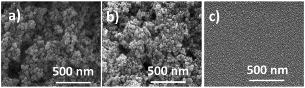 | ||
| Fig. 9 SEM images of surface morphology. (a) ZrO2 on top of cell substrate, (b) addition of 50 passes NiO, (c) 50 passes NiO on glass. | ||
Further analysis of the height variation (from SEM images), as seen in the histogram (Fig. S2, ESI‡), confirmed the lack of major changes in structure on addition of NiO. In both cases the mean height is the same, although addition of NiO must slightly lower the surface roughness as there is a small reduction in the range of feature sizes. The extremely high roughness of the ZrO2 layer leads to a large amount of scattered light, so there is only a very small amount of reflected light. Addition of NiO to the ZrO2 substrate made very little difference (σ = 0.01) to either reflection or transmission over the range 350 nm to 1000 nm for 0 to 24 passes of deposited NiO. At 50 passes there was a small 5% increase in transmission, probably due to the reduced surface roughness and hence decreasing the likelihood of incident light being trapped within the substrate.
Changes in cell behaviour (as discussed later) and XRD data established the presence of NiO in the C-PSC. To confirm that the outside coating is predominately NiO the surface sensitive technique of XPS was used.
XPS confirmed NiO was on the sample surface, but that although there was a decrease in the Zr 3d signal mirroring the increased amount of NiO deposited, there was still about 20% Zr on the surface for 50 passes (Fig. 10). Similarly, although not as well defined the Ni 2p signal showed a corresponding increase in intensity. The mesoporous nature of the ZrO2 and NiO layers led to a small (<2%) Ti 2p signal about 458 eV in the wide scan from the underlying TiO2 layer.
 | ||
| Fig. 10 XPS high resolution spectra of NiO deposited over ZrO2. (A) Zr 3d. (a) No NiO deposition, (b) 20 passes NiO, (c) 50 passes NiO, (B) Ni 2p3/2 (a) 50 passes NiO, (b) 24 passes NiO, (c) 16 passes NiO. | ||
As before for deposition directly on glass the Ni 2p3/2 high resolution scan showed the same distinct peaks and no signal relating to nickel metal. However, the peaks are shifted to a higher binding energy by ca. 0.3 eV, which may be due to a change in crystallite size.43,44 Also, there was a small change in the relative intensities of particularly the cd9L and d8:cd9L emissions. The definition and intensity of the higher energy peak (854.4 eV – cd9L) is greatest for the greater number of passes hence NiO concentration and as that for NiO on glass, while it is least for the lowest number of passes. As discussed earlier this may reflect the changing balance of Ni3+ to Ni2+ within the films and imply that a larger number of passes of the substrate under the coater head led to a higher relative concentration of Ni3+.
Cell performance
Cells were fabricated with a range of FACVD deposited NiO layers with different thickness. Comparisons were made to both a sample treated with the flame process but no NiO and a reference control sample deposited without the additional NiO layer. Two sets of cells were tested with both lower passes (Set 1) for NiO (4 to 12) so definitely individual islands of deposition and transitioning to high number of passes (Set 2) where the NiO would be more compact and transitioning to a more continuous layer.A control sample was fabricated at the same time as each set of experiments so that not only exactly the same solutions were used in each set, but subject to the same environments (for temperature and humidity) and handling procedures. As can be seen the control in set 1 has a slightly lower fill factor, FF and current density, Jsc, which led to a Power Conversion Efficiency, PCE, average of 8.09 ± 0.29% rather than 9.08 ± 0.22% as in set 2. However, the trends within each set are still valid.
For set 1 (4 pass to 12 pass) the cell efficiency increased along with the Jsc and open circuit voltage, Voc, while there was a gradual decrease in average FF (Fig. 11a). For set 2 (16 pass to 24 passes) Jsc, Voc and FF all decreased with increasing NiO thickness and contributed to the reducing PCE (Fig. 11b). In general, there was more variation in values for set 1, particularly for the FF, which may explain the apparent change of trend.
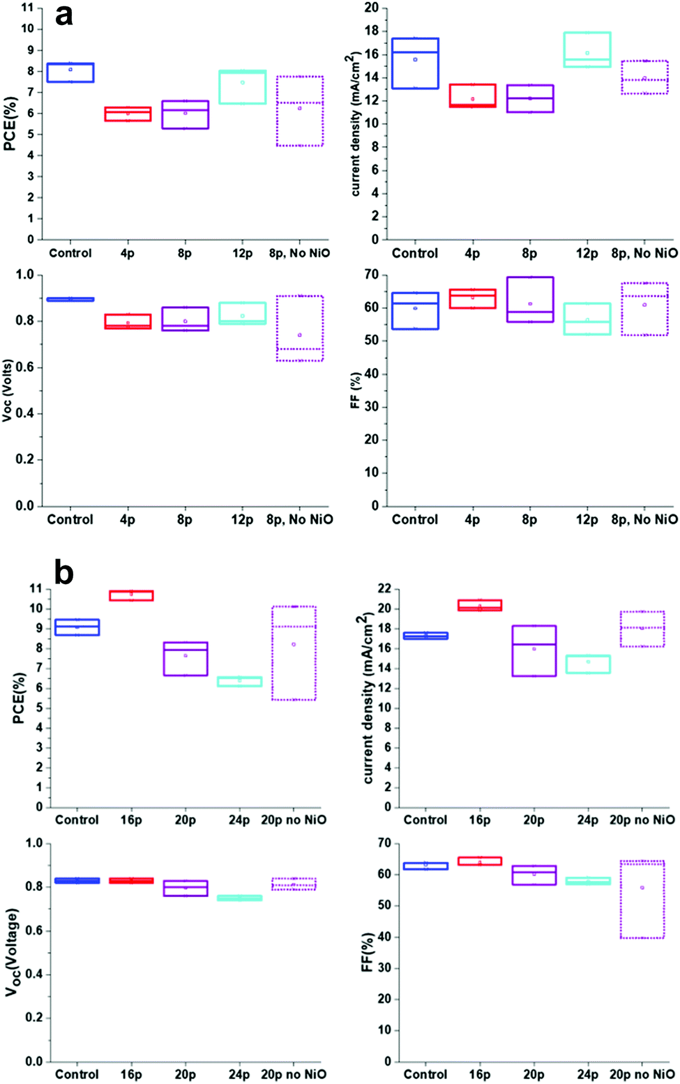 | ||
| Fig. 11 (a) Set 1 – cell characteristic box plots for different thicknesses of FACVD NiO in C-PSC's. (b) Set 2 – cell characteristic box plots for different thicknesses of FACVD NiO in C-PSC's. | ||
The samples exposed to the flame and no NiO deposition performed the worst in terms of variability, but with limited average efficiency changes between this and the comparable NiO coated samples. For set 1 the PCE values were (6.02 ± 0.39)% and (6.24 ± 0.96)% for 8 passes under the flame for with and without NiO respectively. Set 2 with 20 passes under the flame gave (7.64 ± 0.50)% with NiO and (8.23 ± 1.43)% without.
The variability may be due to damage to the cell via the flame, but as discussed earlier there were only very limited changes detected in the preceding layers. Possibly there has been a re-sintering of the layers leading to pore size changes and hence less contact between perovskite and charge carriers. Only at 12 passes, where the film will still be isolated islands, but increasing area did the efficiency start to reach that of the control. At 16 passes of NiO the efficiency of the cell surpassed that of the control with a maximum efficiency of 10.91% and an average of (10.73 ± 0.15)% opposed to (9.08 ± 0.22)% for the control. Its thickness or more precisely island height was estimated from NiO deposition directly on glass as 17 nm (σ = 2 nm). The lack of improvement beyond 16 passes with the FACVD NiO may be due to the film becoming too compact, so no longer porous enough for the perovskite to percolate through the scaffold or changes to pore size and hence less efficient capillary action.
The biggest contribution to the increased cell efficiency at 16 passes of NiO was from the current density, Jsc with a small contribution from the FF. The large gain in Jsc from (17.30 ± 0.15)% for the control (no NiO) to (20.28 ± 0.32)% with NiO is mainly affected by the TiO2/perovskite interface45 and/or the quality of perovskite crystallinity and hence light absorption.46 As the TiO2 is identical in both types of cell it is more likely that the porous nature of the NiO also acts as a template and helps direct the perovskite crystallisation. As demonstrated earlier in this paper the sizing of the NiO islands, hence pore size was directly determined by the number of deposition passes. Larger pores have been reported47 to be more favourable for perovskite infiltration and crystallisation giving larger grains and hence a reduction in grain boundaries which adversely affect cell transport properties.
An improvement in Voc is normally due to a reduction in non-radiative losses and better charge transport. At 16 passes of NiO deposition it is likely that the porosity is at the optimum level for efficiency of perovskite percolation through the layers with better contact at the NiO – perovskite interface and hence improved charge transfer.
Perovskite cells using mesoporous NiO have also been recently reported by Wang et al.48 Here they used a more cumbersome two stage batch electrochemical deposition and thermal annealing process to produce mesoporous NiO, unlike our single stage FACVD process. Similarly, they saw an increase in film density with deposition time and related optimum cell efficiency with thickness and porosity. The perovskite cell structure is not directly comparable, with a spun coated PCBM ETL and a much thicker NiO film (54 nm opposed 17 nm), but they achieved a high efficiency of 17.8%, albeit with an extremely small active area of 0.25 cm2. Our cell active area was at least double this and as previously reported, the cell efficiency decreases substantially with increasing size of active area with for example Chen et al. reporting a 10% reduction in PCE on changing from a 0.09 cm2 to a 1.02 cm2 cell.37
Looking more closely at literature C-PSC type cells our champion device (PCE 10.91%, Jsc 20.9 mA cm−2, FF 65.5%, Voc 836 mV) compared well with the maximum values reached by Mei et al.2 (11.6%, 21.1 mA cm−2, 65.0%, 843 mV). Although Mei used a smaller cell size (0.5 cm2, aperture size 0.07 cm2) and thicker ZrO2 (2 μm opposed to 1.35 ± 0.15 μm). Both these factors can substantially increase PCE. As the ZrO2 layer gets thicker it more effectively separates the C electrode from the TiO2 layer, which reduces recombination so increases Voc and hence improves PCE. For example, Priyadarshi et al.49 reported an increase in efficiency from 7.81% to 9.69% when increasing the ZrO2 thickness from 1.4 μm to 2.1 μm in similar type of C-PSC. Another more recent report47 for C-PSC gave similar Jsc, but lower FF for a PCE of (8.72 ± 1.21)%, although with a smaller device size of 0.14 cm2 and thinner ZrO2 layer (600 nm).
Conclusions
Polycrystalline, mesoporous NiO has been deposited by atmospheric pressure FACVD. Production of a less reducing flame via use of lower propane and increased air in the combustion flame led to more compact films with smaller particle sizes and higher crystallinity. After 50 passes under the lean flame NiO films deposited on ZrO2 were still porous with both Ni and Zr (20%) present on the surface. Optimisation of NiO layer thickness (16 passes, 17 nm thick) and porosity, led to mesoporous carbon perovskite cells with enhanced efficiency reaching 10.91% over that of the control cell (no NiO) maximum of 9.45%.We have demonstrated a low cost, single stage route to large area in-line deposition for NiO, which has been incorporated within C-PSC's, which themselves have been produced by methods with commercial potential.
Conflicts of interest
There are no conflicts to declare.Acknowledgements
HY and JLH received funding from the European Union's Horizon 2020 Research and Innovation programme under grant agreement No. 653296 (CHEOPS). SM, DR, and TW received funding from the UKRI Global Challenge Research Fund project, SUNRISE (EP/P032591/1). XPS data collection was performed at the EPSRC National Facility for XPS (‘HarwellXPS’), operated by Cardiff University and UCL, under contract No. PR16195. G. Parr, Salford Analytical Services provided the SEM images.References
- C. Zuo, H. J. Bolink, H. Han, J. Huang, D. Cahen and L. Ding, Adv. Sci., 2016, 3, 1500324 CrossRef PubMed.
- A. Mei, X. Li, L. Liu, Z. Ku, T. Liu, Y. Rong, M. Xu, M. Hu, J. Chen, Y. Yang, M. Grätzel and H. Han, Science, 2014, 345, 295 CrossRef CAS PubMed.
- G. Grancini, C. Roldán-Carmona, I. Zimmermann, E. Mosconi, X. Lee, D. Martineau, S. Narbey, F. Oswald, F. De Angelis, M. Grätzel and M. K. Nazeeruddin, Nat. Commun., 2017, 8, 15684 CrossRef CAS PubMed.
- Y. Hu, S. Si, A. Mei, Y. Rong, H. Liu, X. Li and H. Han, Sol. RRL, 2017, 1, 1600019 CrossRef.
- F. De Rossi, J. A. Baker, D. Beynon, K. E. A. Hooper, S. M. P. Meroni, D. Williams, Z. Wei, A. Yasin, C. Charbonneau, E. H. Jewell and T. M. Watson, Adv. Mater. Technol., 2018, 3, 1800156 CrossRef.
- D. Burkitt, J. Searle and T. Watson, R. Soc. Open Sci., 2018, 5, 172158 CrossRef PubMed.
- C. Zuo, A. D. Scully, D. Vak, W. Tan, X. Jiao, C. R. McNeill, D. Angmo, L. Ding and M. Gao, Adv. Energy Mater., 2019, 9, 1803258 CrossRef.
- J. Borchert, R. L. Milot, J. B. Patel, C. L. Davies, A. D. Wright, L. Martínez Maestro, H. J. Snaith, L. M. Herz and M. B. Johnston, ACS Energy Lett., 2017, 2, 2799 CrossRef CAS.
- M. Bag, Z. Jiang, L. A. Renna, S. P. Jeong, V. M. Rotello and D. Venkataraman, Mater. Lett., 2016, 164, 472 CrossRef CAS.
- C. Zuo, D. Vaka, D. Angmo, L. Ding and M. Gao, Nano Energy, 2018, 46, 185 CrossRef CAS.
- K. Hwang, Y.-S. Jung, Y.-J. Heo, F. H. Scholes, S. E. Watkins, J. Subbiah, D. J. Jones, D.-Y. Kim and D. Vak, Adv. Mater., 2015, 27, 1241 CrossRef CAS PubMed.
- X. Xu, Z. Liu, Z. Zuo, M. Zhang, Z. Zhao, Y. Shen, H. Zhou, Q. Chen, Y. Yang and M. Wang, Nanolett., 2015, 15, 2402 CrossRef CAS PubMed.
- S. Liu, W. Huang, P. Liao, N. Pootrakulchote, H. Li, J. Lu, J. Li, F. Huang, X. Shai, X. Zhao, Y. Shen, Y.-B. Cheng and M. Wang, J. Mater. Chem. A, 2017, 5, 22952 RSC.
- D. W. Sheel, L. A. Brook and H. M. Yates, Chem. Vap. Deposition, 2008, 14, 14 CrossRef CAS.
- H. M. Yates, P. Sheel, J. L. Hodgkinson, M. E. A. Warwick, S. O. Elfakhri and H. A. Foster, Surf. Coat. Technol., 2017, 324, 201 CrossRef CAS.
- D. S. Saranin, V. N. Mazov, L. O. Luchnikov, D. A. Lypenko, P. A. Gostishev, D. S. Muratov, D. A. Podorny, D. M. Migunov, S. I. Didenko, M. N. Orlova, D. V. Kuznetsov, A. R. Tameev and A. Di Carlo, J. Mater. Chem. C, 2018, 6, 6179 RSC.
- Z. Zhang, S. Chen, P. Li, H. Li, J. Wu, P. Hu and J. Wang, Funct. Mater. Lett., 2018, 11, 1850035 CrossRef CAS.
- A. Saenz-Trevizo, P. Amezaga-Madrid, P. Piza-Ruiz, O. Solis-Canto, C. Ornelas-Gutierrez, S. Perez-Garcia and M. Miki-Yoshida, J. Alloys Compd., 2014, 615, 5375 CrossRef.
- H. M. Yates, L. A. Brook, D. W. Sheel, I. B. Ditta, A. Steele and H. A. Foster, Thin Solid Films, 2008, 517, 517 CrossRef CAS.
- http://www.mtixtl.com/FTO-252522TEC7-25.aspx .
- S. M. P. Meroni, Y. Mouhamad, F. De Rossi, A. Pockett, J. Baker, R. Escalante, J. Searle, M. J. Carnie, E. Jewell, G. Oskam and T. M. Watson, Sci. Technol. Adv. Mater., 2018, 19, 1 CrossRef CAS.
- https://imagej.nih.gov/ij/download.html .
- B. D. Cullity, Elements of X-Ray Diffraction, 2nd edn, Addison-Wesley, Reading, Mass, 1978 Search PubMed.
- J. Tang, D. Jiao, L. Zhang, X. Zhang, X. Xu, C. Yao, J. Wu and Z. Lan, Sol. Energy, 2018, 161, 100 CrossRef CAS.
- Y. Bai, H. Chen, S. Xiao, Q. Xue, T. Zhang, Z. Zhu, Q. Li, C. Hu, Y. Yang, Z. Hu, F. Huang, K. S. Wong, H.-L. Yip and S. Yang, Adv. Funct. Mater., 2016, 26, 2950 CrossRef CAS.
- J. H. Kim, P.-W. Liang, S. T. Williams, N. Cho, C.-C. Chueh, M. S. Glaz, D. S. Ginger and A. K.-Y. Jen, Adv. Mater., 2015, 27, 695 CrossRef CAS PubMed.
- X. Yin, Z. Yao, Q. Luo, X. Dai, Y. Zhou, Y. Zhang, Y. Zhou, S. Luo, J. Li, N. Wang and H. Lin, ACS Appl. Mater. Interfaces, 2017, 9, 2439 CrossRef CAS PubMed.
- M. Afzaal, H. M. Yates, A. Walter and S. Nicolay, IEEE J. Photovoltaics DOI:10.1109/JPHOTOV.2019.2927927.
- S. Yueyan, Z. Zhiyang and Y. Xiaoji, Sol. Energy Mater. Sol. Cells, 2002, 71, 51 CrossRef.
- S. Seo, I. J. Park, M. Kim, S. Lee, C. Bae, H. S. Jung, N.-G. Park, J. Y. Kim and H. Shin, Nanoscale, 2016, 8, 11403 RSC.
- M. Z. Sialvi, R. J. Mortimer, G. D. Wilcox, A. M. Teridi, T. S. Varley, K. G. U. Wijayantha and C. A. Kirk, ACS Appl. Mater. Interfaces, 2013, 5, 5675 CrossRef CAS PubMed.
- J. L. Hodgkinson and H. M. Yates, Proc. PVSAT 14, The Solar Energy Soc., London, UK, April 2018. P81–P84.
- J. Chastain and R. C. King, Handbook of X-Ray Photoelectron Spectroscopy, Physical Electronic Inc., New York, 1995 Search PubMed.
- X. Geng, D. Lahem, C. Zhang, C.-J. Li, M.-G. Olivier and M. Debliquy, Ceram. Int., 2019, 45, 4253 CrossRef CAS.
- E. Turgut, O. Coban, S. Santa, S. Tuzemen and M. Yildirm, Appl. Surf. Sci., 2019, 435, 880 CrossRef.
- A. G. Marrani, V. Novelli, S. Sheehan, D. P. Dowling and D. Dini, ACS Appl. Mater. Interfaces, 2014, 6, 143 CrossRef CAS PubMed.
- W. Chen, Y. Wu, Y. Yue, J. Liu, W. Zhang, X. Yang, H. Chen, E. Bi, I. Ashraful, M. Grätzel and L. Han, Science, 2015, 350, 944 CrossRef CAS PubMed.
- N. D. Hoa, P. V. Tong, C. M. Hung, N. V. Duy and N. V. Hieu, Int. J. Hydrogen Energy, 2018, 43, 9446 CrossRef.
- J. H. Park, J. Seo, S. Park, S. S. Shin, Y. C. Kim, N. J. Jeon, H.-W. Shin, T. K. Ahn, J. H. Noh, S. C. Yoon, C. S. Hwang and S. I. Seok, Adv. Mater., 2015, 27, 4013 CrossRef CAS PubMed.
- Y. J. Sun, T. Egawa, L. Y. Zhang and X. Yao, Jpn. J. Appl. Phys., 2002, 41, L1389 CrossRef CAS.
- J. Guillot, A. Jouaiti, B. Domenichini, O. Heintz, S. Zerkout, A. Mosser and S. Bourgeois, Surf. Interface Anal., 2002, 34, 577 CrossRef.
- D. W. Zeng, K. C. Yung and C. S. Xie, Surf. Coat. Technol., 2002, 153, 210 CrossRef CAS.
- I. M. Arabatzis, T. Stergiopoulos, M. C. Bernard, D. Labou, S. G. Neophytides and P. Falaras, Appl. Cat. B, 2003, 42, 187 CrossRef CAS.
- M. W. Xu, S. J. Bao and X. G. Zhang, Mater. Lett., 2005, 59, 2194 CrossRef CAS.
- J. Baker, K. Hooper, S. Meroni, A. Pocket, J. McGettrick, Z. Wei, R. Escalante, G. Oskam, M. Carnie and T. Watson, J. Mater. Chem. A, 2017, 5, 18643 RSC.
- Z. H. Liu, A. L. Zhu, F. S. Cai, L. M. Tao, Y. H. Zhou, Z. X. Zhao, Q. Chen, Y. B. Cheng and H. P. Zhou, J. Mater. Chem. A, 2017, 5, 6597 RSC.
- Z. Meng, D. Guo, J. Yu and K. Fan, Appl. Surf. Sci., 2018, 430, 632 CrossRef CAS.
- T. Wang, D. Ding, X. Wang, R. Zeng, H. Liu and W. Shen, ACS Omega, 2018, 3, 18434 CrossRef CAS PubMed.
- A. Priyadarshi, A. Bashir, J. T. Gunawan, L. J. Haur, A. Bruno, Z. Akhter, N. Mathews and S. G. Mhaisalkar, Energy Technol., 2017, 5, 1866 CrossRef CAS.
Footnotes |
| † The dataset for this work can be found at https://doi.org/10.17866/rd.salford.9608828.v1 |
| ‡ Electronic supplementary information (ESI) available. See DOI: 10.1039/c9tc03922h |
| This journal is © The Royal Society of Chemistry 2019 |