
 Open Access Article
 This Open Access Article is licensed under a
 Creative Commons Attribution 3.0 Unported Licence
Discrete color centers in two-dimensional hexagonal boron nitride induced by fast neutron irradiation†
Hui
Zhang
 *ab,
Mu
Lan
ab,
Ge
Tang
a,
Feiliang
Chen
ab,
Zhiwen
Shu
c,
Fengxiang
Chen
d and
Mo
Li
*ab
*ab,
Mu
Lan
ab,
Ge
Tang
a,
Feiliang
Chen
ab,
Zhiwen
Shu
c,
Fengxiang
Chen
d and
Mo
Li
*ab
aMicrosystem and Terahertz Research Center, China Academy of Engineering Physics, Chengdu 610200, China. E-mail: zhanghui@mtrc.ac.cn; limo@mtrc.ac.cn
bInstitute of Electronic Engineering, China Academy of Engineering Physics, Chengdu 610200, China
cCollege of Mechanical and Vehicle Engineering, Hunan University, Changsha 410082, China
dSchool of Science, Wuhan University of Technology, Wuhan 430070, China
First published on 20th September 2019
Abstract
Color centers in two-dimensional hexagonal boron nitride, as promising room-temperature quantum emitters, have attracted much research interest. Many methods have been performed to create color centers on hBN, but the induced color centers tend to aggregate at flake edges or grain boundaries. In this paper, fast neutron irradiation was implemented to generate color centers with a homogeneous and discrete distribution on 2D hBN multilayers. The density of induced color centers positively correlated with the neutron dose, and within an appropriate neutron dose range, the spectral uniformity of the induced color centers could be maintained well. In addition, first-principle calculations were performed to explore the atomic origin of the observed color centers, and the VB3N1 defect was in good agreement with our experimental results.
Introduction
Quantum light, such as single photon and correlated photon pair, is urgently needed in quantum information processing and quantum sensing. Local defects in solids, the so-called “color centers”, as an artificial atomic system, are promising candidates for quantum light sources, particularly in terms of miniaturization and integration.1–4 Among them, color centers in two-dimensional (2D) structure hexagonal boron nitride (hBN) were proved to have bright, multicolor, stable emission even at a temperature higher than 800 K.5–7 By now, a series of methods, such as annealing,8,9 chemical etching,10 ion implantation,11 and electron irradiation,8,11 has been used in generating color centers in 2D hBN. However, the generation of color centers by the above methods seems to highly rely on intrinsic defects and dangling bonds near flake edges or grain boundaries, so the induced color centers tend to aggregate locally, which is not useful for the applications of quantum light sources. To generate color centers with reduced boundary aggregation, high-energy electrons with an energy of ∼2 MeV were used to irradiate 2D hBN by Duong et al.12 Their results showed that as the kinetic energy of electron irradiation increased, the induced color centers could locate within the hBN flakes rather than just at flake edges or grain boundaries.Neutron irradiation has been proved as a feasible method to generate color centers in hBN powder.13 Because of the large mass and electric neutrality, neutrons can effectively transfer a significant part of their kinetic energy to the atoms and directly form atomic displacements.14,15 So, neutron irradiation with adequate energy can be a promising way to generate discrete color centers in 2D hBN and overcome their aggregation at flake edges or grain boundaries. In this work, we investigated the spatial and spectral features of color centers in hBN multilayers generated by fast neutron irradiation (∼1.2 MeV) with confocal micro-photoluminescence (μ-PL) spectroscopy. Our results suggested that color centers induced by fast neutron irradiation showed a homogeneous and discrete distribution on 2D hBN. The density of color centers positively correlated with the neutron dose, providing a possibility of controllable hBN defect engineering. Besides, the spectral statistical results demonstrated that within an appropriate neutron dose range, the spectral uniformity of the induced color centers could be maintained well, in spite of great changes in quantity of the color centers.
To explore the possible atomic origin of the color centers in hBN, first-principle calculations have been performed by several teams. T. T. Tran et al.,7 X. Li et al.16 and S. A. Tawfik et al.17 used the generalized gradient approximation of Perdew, Burke and Ernzerhof (PBE)18,19 to study various possible point defects in hBN. Their results showed that the NBVN defect had a spin-polarized transition of ∼2 eV. L. Weston et al.20 and A. Sajid et al.21 used the Heyd–Scuseria–Ernzerhof hybrid functional (HSE06)22,23 method to study hBN defects, and they concluded that BN antisite (2.13 eV), boron self-interstitials (1.88 eV), and VNCB (2.08 eV) were also possible point-defect types of color centers in hBN. In this work, first-principle calculations with the HSE06 method were also performed to explore the atomic origin of color centers observed in our experiment, and the VB3N1 defect was found to be in good agreement with our experimental results and could be a promising candidate type of point defect in hBN.
Results and discussion
In this work, hBN multilayers synthesized by a chemical vapor deposition (CVD) method and supplied by Graphene Supermarket were used as the samples. As can be seen in Fig. 1(a), the hBN multilayer was transferred onto a 300 nm thick SiO2/Si substrate and showed a color contrast in the optical microscope image because of the interference effect. The thickness of the multilayer was about 4.9 nm and the atomic force microscopy (AFM) image is given in Fig. 1(b). The fast neutron source used in this work has an average energy of 1.2 MeV and a pulse width of 194 μs. The hBN samples were fixed on three spherical shells around the neutron source, as shown in Fig. 1(c), with different neutron doses of 1.5 × 10¹³ n cm−2 (Sample I), 2.5 × 10¹³ n cm−2 (Sample II), and 1.0 × 10¹⁴ n cm−2 (Sample III), respectively. No annealing process of the hBN samples was carried out before and after the neutron irradiation experiments. To check whether 2D hBN could be maintained after neutron irradiation, Raman spectra of unirradiated and irradiated hBN multilayer samples on SiO2/Si substrates were obtained, using a Horiba LabRAM HR Evolution confocal microscope, with a picosecond pulse 266 nm excitation laser, a 40× reflective objective of 0.5 numerical aperture (NA), and a spectrometer with 800 mm focal length and 2400 g mm−1 grating. As shown in Fig. 1(d), ignoring the Raman signals from SiO2/Si substrates, the Raman characteristic peak of hBN7,10,24 at ∼1374 cm−1 could be found on both unirradiated and irradiated samples, which suggested that the basic structure of 2D hBN was not destroyed by neutron irradiation.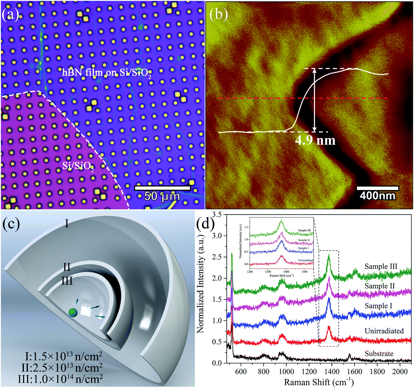 | ||
| Fig. 1 (a) Optical microscopy image of hBN multilayer transferred onto 300 nm SiO2/Si substrates. The dashed line indicated the hBN multilayer edge. The yellow dots were periodic holes on the substrates. (b) The AFM image of the hBN multilayer edge. The white curve showed the height data along the red dashed line. (c) Schematic diagram of the fast neutron irradiation experiments. The hBN samples were fixed on three spherical shells around the the neutron source. The neutron doses on the three spherical shells were I: 1.5 × 10¹³ n cm−2, II: 2.5 × 10¹³ n cm−2, and III: 1.0 × 10¹⁴ n cm−2, respectively. (d) Room-temperature Raman spectra of unirradiated and irradiated hBN multilayer samples on SiO2/Si substrates. All spectra were normalized according to the silicon Raman peak at ∼521.7 cm−1. Details of the hBN Raman peak were shown in the inset. | ||
To investigate the spatial features of color centers induced by fast neutron irradiation, the irradiated samples were characterized with confocal μ-PL scanning. The measurements were carried out using a Witec alpha 300R confocal microscope, with a continuous 532 nm excitation laser, a 100× objective of 0.9 NA, and a spectrometer with 300 mm focal length and 150 g mm−1 grating. As an insulator with an intrinsic band gap of 5.955 eV,25 hBN should be transparent and non-luminescent with 532 nm excitation. As shown in Fig. S1 in the ESI,† the hBN multilayer did not contain obvious color centers before neutron irradiation. After neutron irradiation, two kinds of PL peaks were observed from the irradiated samples, locating at ∼580 nm and ∼630 nm, respectively, which suggested color centers in hBN had been induced by neutron irradiation. 2D spatial mapping of PL integrated intensity was carried out in the wavelength range of 567.5–592.5 nm, indicated by green color, and of 610–650 nm, indicated by red color, as shown in Fig. 2(a)–(c) for Samples I–III, respectively. PL spectra of certain points were chosen and are shown in Fig. 2(d)–(f). Three of them were in green colors labeled as ‘#1–#3’ and the others were in red colors labeled as ‘#4–#6’, respectively. From Fig. 2(a), we can see that a few discrete color centers (marked in green color) emerged in hBN after the neutron irradiation with a dose of 1.5 × 10¹³ n cm−2, without obvious aggregation at multilayer edges or grain boundaries. As shown in Fig. 2(d), the PL emission of these discrete color centers showed narrow peaks at ∼580 nm, which should correspond to the zero phonon line (ZPL)7,12 of color centers. Besides, a kind of nonlocal luminescence with wider linewidth was also found at ∼630 nm, which diffused over nearly the whole sample continuously, so the corresponding color centers should be dense and may be induced by the nonlocal neutron cascading scattering events from hBN multilayer and the substrates.15 With a stronger irradiation dose, the density of green color centers of Sample II exhibited a significant increase and most of them still remained discrete. The spectra in Fig. 2(e) showed that their ZPLs remained sharp and their relative intensity against the nonlocal luminescence at ∼630 nm showed a sensible rise. When the neutron irradiation dose increased to 1.0 × 10¹⁴ n cm−2, the green color centers became continuous and nonlocal, distributing over the whole sample, mixed with the nonlocal luminescence at ∼630 nm, as shown in Fig. 2(c). It can be found in Fig. 2(f) that the emission of ZPLs at ∼580 nm became much broader, similar to that at ∼630 nm. Besides, the luminescence at ∼580 nm upon the etched holes showed a stronger intensity than the other place, which should be caused by the interference of the substrate structure. Notably, the emission at ∼630 nm had a wider linewidth than that at ∼580 nm, which was supposed to be mainly caused by the higher density of color centers. As the color centers were dense, a plurality of them were excited at the same time by one laser spot in the μ-PL measurement. Slight inhomogeneity of matrix surrounding color centers could cause a shift of ZPLs, so broadening from ZPL overlapping could be a probable origin of the wide peaks at ∼630 nm. In addition, ZPLs are often accompanied by phonon-sidebands (PSBs) with wider linewidth.10–12,16 So, it is possible that at the points where the green color centers with ZPL at ∼580 nm occur, the PSBs of the ZPL may also exist and be covered under the wide peak at ∼630 nm, which needs further study. To summarize, fast neutron irradiation can efficiently generate color centers with emission at ∼580 nm on 2D hBN multilayers, and the density of the color centers are positively correlated with the irradiation dose. By controlling the irradiation dose, discrete color centers can be obtained on hBN multilayers, without obvious aggregation at the multilayer edges or grain boundaries.
 | ||
| Fig. 2 2D spatial maps of PL integrated intensity of (a) Sample I, (b) Sample II, and (c) Sample III. Integrated intensities within 567.5–592.5 nm were marked by green color and those within 610–650 nm were marked by red color. The white dashed line indicated the hBN multilayer edges. PL spectra of selected points were shown in (d)–(f), corresponding to the points marked in (a)–(c). All spectra were normalized according to the maximum of PL intensity. The green and red dashed lines indicated the integral intervals centered at 580 nm and 630 nm, respectively. | ||
To compare the spectral features of the discrete color centers induced by varying the neutron irradiation dose, statistical analysis of central wavelength (c) and spectral linewidth (w) for the color centers in Sample I and II was performed. Gaussian fitting was utilized on all the ZPLs at ∼580 nm, as shown in Fig. 2(a) and (b). The statistical distributions of the fitting results are shown in histograms in Fig. 3. Fig. 3(a) shows that the c of ZPLs follows a normal distribution, with the standard deviations of 3.78 nm and 3.85 nm, for Sample I and II, respectively. Fig. 3(b) shows that the w of ZPLs also exhibits a normal distribution, with the standard deviation of 4.94 nm and 5.06 nm, for Sample I and II, respectively. The slight rise of standard deviation of c and w for Sample II suggested that the uniformity of color centers did not deteriorate notably after the quantity of color centers had greatly increased. As for the mean values, c presented a mean of 579.27 nm and 580.81 nm, and w presented a mean of 14.28 nm and 14.89 nm, for Sample I and II, respectively. The relative broadening of the mean w for Sample II may due to the slight aggregation of color centers, as shown in Fig. 2b. In the above statistical analyses, the PL spectra with too weak intensity (amplitude <0.2 cnt) or very abnormal linewidth (w < 0.1 nm or w > 35 nm) were not used, as they mostly came from false fitting caused by spectral noise.
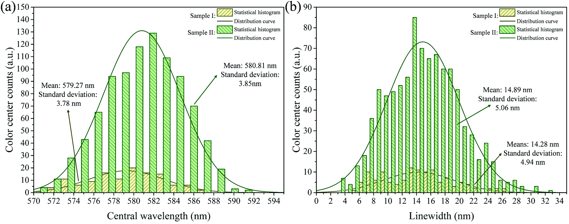 | ||
| Fig. 3 Statistical results of the Gaussian fitting of the ZPLs at ∼580 nm in the corresponding areas of Sample I and II shown in Fig. 2. (a) Histogram of statistical central wavelength of the ZPLs at ∼580 nm. The attached lines showed the fitted normal distribution curves. (b) Histogram of statistical linewidth of the ZPLs at ∼580 nm. The attached lines showed the fitted normal distribution curves. | ||
To explore the possible atomic origin of the observed color centers, first-principle calculations for electronic structures of possible point defects were implemented, with the following specific calculation methods. The Vienna ab initio simulation package26 was used to calculate the electronic properties of point defects in hBN. A plane-wave cutoff of 520 eV was used for all calculations with the generalised gradient approximation18 of the exchange correlation functional proposed by Perdew, Burke and Ernzerhof.19 Spin polarized hybrid density functional methods (HSE06)22,23 were used to get a proper description of the electronic structures. All the geometries were optimized until the Hellman–Feymann Force converged to 0.002 eV Å−1. The DFT-D3 method of Grimme27 was employed to describe the van der Waals interactions between the adjacent layers. AA′ stacking28,29 pristine hBN was optimized using a conventional cell and 13 × 13 × 5 Monkhorst–Pack grid for Brillouin zone sampling. The calculated lattice parameter was 2.51 Å (the error was less than 0.3% with regard to the experimental value) and van der Waals gap was 3.37 Å (the error was less than 1% with regard to the experimental value). The calculated band structure of hBN is shown in Fig. 4(a). It indicated that hBN is an indirect bandgap semiconductor with a band gap of 5.57 eV, which was slightly underestimated compared with the experimental value of 5.955 eV.25
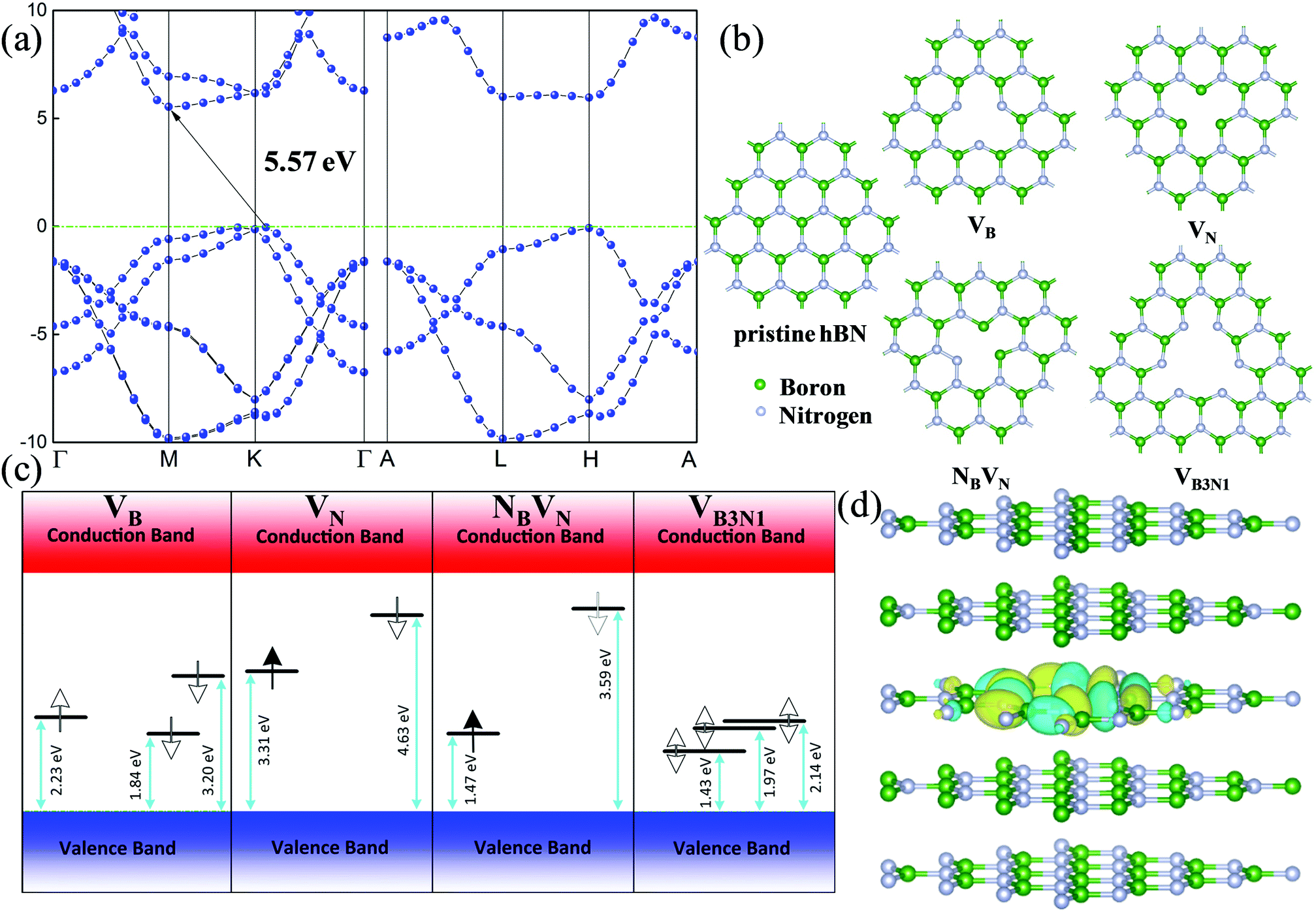 | ||
| Fig. 4 (a) Simulated band structure of hBN with HSE06 hybrid functional method. The green dashed line represented the Fermi level. (b) Schematics of pristine hBN and four possible point defects. (c) The corresponding electronic structures of the point defects shown in (b). Solid/hollow arrows indicated occupied/unoccupied states, and upward/downward arrows indicated the spins were up/down. (d) The spatial distribution of the defect level wave function in the VB3N1 defect calculation. | ||
The defects were located in a 5 × 5 × 2 supercell, respectively. The atomic structures of pristine hBN and four possible point defects are shown in Fig. 4(b), with corresponding electronic structures of the point defects given in Fig. 4(c). It can be seen that the two possible electron transitions of 1.97 eV and 2.14 eV of the VB3N1 defect were in good agreement with the luminescence peaks around 630 nm and 580 nm in our experimental results, respectively. In addition, the transition energy of 1.84 eV in the VB defect could also be related to the luminescence peak near 630 nm. It is worth noting that with different calculation methods adopted, the calculated electronic structures of NBVN defects7,16,17,21 changed greatly, and were not consistent with our experimental results. The spatial distribution of the defect level wave function of the VB3N1 defect calculation is shown in Fig. 4(d). It can be seen that the wave function was confined near one atom layer. Therefore, the number of atomic layers had little impact on the calculation results, which was consistent with the previous reports.7
Conclusions
In this work, fast neutron irradiation (∼1.2 MeV) was proved as an efficient way to generate discrete color centers with ZPL at ∼580 nm in 2D hBN multilayers. The distribution of these color centers showed good discreteness and almost no dependence on multilayer edges and grain boundaries. The density of the color centers positively correlated with the neutron dose, providing a possibility of controllable hBN defect engineering for further single-photon source applications. In addition, the spectral statistical results demonstrated that within an appropriate neutron dose range, in spite of great changes in the quantity of the induced color centers, their spectral uniformity could be maintained well. Finally, first-principle calculations suggested that the discrete color centers with ZPL at ∼580 nm may originate from VB3N1 defects. This work may provide a promising procedure for hBN defect engineering and a helpful understanding of the origin of color centers in hBN.Conflicts of interest
There are no conflicts to declare.Acknowledgements
We would like to thank China Fast Burst Reactor-II of CAEP for supporting neutron irradiation. This work was supported by the National Natural Science Foundation of China (No. 61705203) and the Science Challenge Project (No. TZ2016003).References
- I. Aharonovich, D. Englund and M. Toth, Nat. Photonics, 2016, 10, 631–641 CrossRef CAS.
- J. Vukovi, J. L. O'Brien and A. Furusawa, Nat. Photonics, 2009, 3, 687–695 CrossRef.
- M. Atatüre, D. Englund, N. Vamivakas, S.-Y. Lee and J. Wrachtrup, Nat. Rev. Mater., 2018, 3, 38–51 CrossRef.
- D. D. Awschalom, L. C. Bassett, A. S. Dzurak, E. L. Hu and J. R. Petta, Science, 2013, 339, 1174–1179 CrossRef CAS PubMed.
- T. T. Tran, C. Elbadawi, D. Totonjian, C. J. Lobo, G. Grosso, H. Moon, D. R. Englund, M. J. Ford, I. Aharonovich and M. Toth, ACS Nano, 2016, 10, 7331–7338 CrossRef CAS PubMed.
- M. Kianinia, B. Regan, S. A. Tawfik, T. T. Tran, M. J. Ford, I. Aharonovich and M. Toth, ACS Photonics, 2017, 4, 768–773 CrossRef CAS.
- T. T. Tran, K. Bray, M. J. Ford, M. Toth and I. Aharonovich, Nat. Nanotechnol., 2016, 11, 37–41 CrossRef CAS PubMed.
- A. L. Exarhos, D. A. Hopper, R. R. Grote, A. Alkauskas and L. C. Bassett, ACS Nano, 2017, 11, 3328–3336 CrossRef CAS PubMed.
- A. W. Schell, M. Svedendahl and R. Quidant, Adv. Mater., 2018, 30, 1704237 CrossRef PubMed.
- N. Chejanovsky, M. Rezai, F. Paolucci, Y. Kim, T. Rendler, W. Rouabeh, F. Fávaro de Oliveira, P. Herlinger, A. Denisenko and S. Yang, Nano Lett., 2016, 16, 7037–7045 CrossRef CAS PubMed.
- S. Choi, T. T. Tran, C. Elbadawi, C. Lobo, X. Wang, S. Juodkazis, G. Seniutinas, M. Toth and I. Aharonovich, ACS Appl. Mater. Interfaces, 2016, 8, 29642–29648 CrossRef CAS PubMed.
- H. N. M. Duong, M. A. P. Nguyen, M. Kianinia, T. Ohshima, H. Abe, K. Watanabe, T. Taniguchi, J. H. Edgar, I. Aharonovich and M. Toth, ACS Appl. Mater. Interfaces, 2018, 10, 24886–24891 CrossRef PubMed.
- J. Toledo, D. De Jesus, M. Kianinia, A. Leal, C. Fantini, L. Cury, G. Sáfar, I. Aharonovich and K. Krambrock, Phys. Rev. B, 2018, 98, 155203 CrossRef CAS.
- J. Eapen, R. Krishna, T. D. Burchell and K. Murty, Mater. Res. Lett., 2014, 2, 43–50 CrossRef CAS.
- R. Walker, T. Shi, E. Silva, I. Jovanovic and J. Robinson, Phys. Status Solidi A, 2016, 213, 3065–3077 CrossRef CAS.
- X. Li, G. D. Shepard, A. Cupo, N. Camporeale, K. Shayan, Y. Luo, V. Meunier and S. Strauf, ACS Nano, 2017, 11, 6652–6660 CrossRef CAS PubMed.
- S. A. Tawfik, S. Ali, M. Fronzi, M. Kianinia, T. T. Tran, C. Stampfl, I. Aharonovich, M. Toth and M. J. Ford, Nanoscale, 2017, 9, 13575–13582 RSC.
- P. E. Blöchl, Phys. Rev. B: Condens. Matter Mater. Phys., 1994, 50, 17953 CrossRef PubMed.
- J. P. Perdew, K. Burke and M. Ernzerhof, Phys. Rev. Lett., 1996, 77, 3865–3868 CrossRef CAS PubMed.
- L. Weston, D. Wickramaratne, M. Mackoit, A. Alkauskas and C. Van de Walle, Phys. Rev. B, 2018, 97, 214104 CrossRef CAS.
- A. Sajid, J. R. Reimers and M. J. Ford, Phys. Rev. B, 2018, 97, 064101 CrossRef CAS.
- J. Heyd, G. E. Scuseria and M. Ernzerhof, J. Chem. Phys., 2003, 118, 8207–8215 CrossRef CAS.
- A. V. Krukau, O. A. Vydrov, A. F. Izmaylov and G. E. Scuseria, J. Chem. Phys., 2006, 125, 224106 CrossRef PubMed.
- R. Geick, C. Perry and G. Rupprecht, Phys. Rev., 1966, 146, 543 CrossRef CAS.
- G. Cassabois, P. Valvin and B. Gil, Nat. Photonics, 2016, 10, 262 CrossRef CAS.
- G. Kresse and J. Furthmüller, Phys. Rev. B: Condens. Matter Mater. Phys., 1996, 54, 11169 CrossRef CAS PubMed.
- H. Krieg, J. Antony, S. Ehrlich and S. Grimme, J. Chem. Phys., 2010, 132, 154104 CrossRef PubMed.
- R. Pease, Nature, 1950, 165, 722 CrossRef CAS PubMed.
- G. Constantinescu, A. Kuc and T. Heine, Phys. Rev. Lett., 2013, 111, 036104 CrossRef PubMed.
Footnote |
| † Electronic supplementary information (ESI) available: The 2D spatial map of PL integrated intensity of an untreated sample and ab initio molecular dynamics simulation results of VB3N1. See DOI: 10.1039/c9tc03695d |
| This journal is © The Royal Society of Chemistry 2019 |