
 Open Access Article
 This Open Access Article is licensed under a Creative Commons Attribution-Non Commercial 3.0 Unported Licence
Structural coloration by inkjet-printing of optical microcavities and metasurfaces†
Samim
Sardar
,
Pawel
Wojcik
,
Evan S. H.
Kang
,
Ravi
Shanker
and
Magnus P.
Jonsson
 *
*
Laboratory of Organic Electronics, Linköping University, SE-601 74 Norrköping, Sweden. E-mail: magnus.jonsson@liu.se
First published on 24th June 2019
Abstract
Structural color generation by plasmonic and other means has attracted significant interest as a solution to avoid inks based on dyes. Prominent advantages include better robustness compared with organic dyes while also providing high chromaticity and brightness in ultrathin films. However, lack of cheap and scalable fabrication techniques has so far limited structural coloration to only a few applications and functional devices. Here, we demonstrate reflective (plasmonic) structural coloration at high resolution by inkjet printing on non-patterned surfaces. The method is flexible, scalable to large areas, and avoids complicated or costly fabrication steps. Optical microcavities on flexible plastic substrates were made starting with an inkjet-printed silver film as a bottom mirror. Inkjet-printed organic dielectric micropixels then served as the spacer layer, resulting in optical microcavities with reflective structural colors after coating with a thin semi-transparent metallic top layer. Optimization of ink formulation allowed for uniform pixels with minimum coffee stain effects as well as control of spacer thickness (around 50–150 nm) and color by varying the solid content of the ink. We investigate the possibility to obtain red, green and blue (RGB) pixels and demonstrate the improvement of particularly the blue coloration using wavelength-dependent plasmon absorption of gold nanoislands as a top mirror. Inkjet printing of optical microcavities and plasmonic cavities may find use in various applications, such as reflective displays in color.
1. Introduction
Structural color generation based on interaction of light with optical cavities, photonic crystals and nanostructures has gained tremendous interest as a solution for ink-free color production.1–5 Nature itself provides beautiful structural coloration in birds and insects6,7 and these vivid and vibrant natural colors have inspired biomimetic color generation.8–12 Compared with traditional concepts based on pigments or dyes, structural coloration generated from physical structures provides several advantages, such as high resolution,13 high chromaticity,14 and not least excellent resistance to fading.15,16 Plasmonic colors based on metallic nanostructures and metasurfaces have attracted particular interest owing to the possibility to create stable ultrathin high-resolution color images.17–21 Such systems can be 1–2 orders of magnitude thinner than pigment-based systems, favouring integration and miniaturization of devices.22 Recent reports also demonstrate dynamic control of structural colors,2 including the use of conjugated electrochromic polymers on plasmonic metasurfaces for electronic paper in color.23–25Despite several advantages of structural color generation over dye technology, it remains challenging to manufacture large-scale structural color patterns in an economically affordable way. Most plasmonic color patterns have so far been pre-designed and printed either by e-beam lithography (EBL)13,26–28 or focused ion beam (FIB) lithography,29,30 both expensive and not suitable for up-scaling. Efforts have been devoted to overcoming these challenges, including laser post-writing on nanoimprinted plasmonic metasurfaces,21 replication using master patterns,31,32 photolithography combined with self-assembly nanofabrication,23,24 laser-induced photothermal patterning of gold nanorods,33 and assembling plasmonic nanoparticles onto predefined binding sites.18 However, it remains challenging to directly print structural colors without the involvement of pre- or post-patterning. Such direct printing could enable rapid large-scale production of structurally colored images based on simple digital image inputs.
Inkjet printing is a versatile tool for printing large-scale patterns while maintaining high spatial resolution. It is convenient, cost-effective and does not require any patterned masks. Inkjet printing was recently applied for printing of dielectric nanospheres that assembled into photonic crystals to display structural color.34–40 Titanium dioxide nanoparticles were inkjet-printed to generate thickness-dependent interference colors for custom input images41 and also onto a holographic paper with preserved diffractive colors.42 Other reports utilized pre-patterned substrates. For example, Jiang et al.43 obtained structural colors by inkjet printing silver nanoparticles on substrates pre-patterned with polymer nanostructures. Even more recently, inkjet-printing was used to deposit (colorless) titanium dioxide nanoparticles onto subwavelength polymer gratings to achieve red, green and blue structurally colored pixels.44 These recent reports exemplify the growing interest in this emerging field and highlight the importance of addressing the several remaining challenges for inkjet-based fabrication of structural colors.
In this work, we present the fabrication of microcavities and plasmonic structural colors on non-patterned surfaces using inkjet printing, which is scalable to large areas and avoids complicated fabrication steps. The device geometry is based on a metal–insulator–metal/metasurface configuration (see Fig. 1), with reflective structural color tuned by Fabry–Pérot interference and wavelength-dependent plasmon absorption. The protocol starts with inkjet-printing of a bottom mirror silver film (∼500 nm thick) on a flexible PET substrate. Next, we inkjet-printed arrays of transparent organic photoresist (SU8) micropixels and completed the structure by deposition of a semitransparent thin metal layer. This creates a Fabry–Pérot microcavity with structurally colored reflection that is sensitive to the thickness of the spacer layer of each pixel. In turn, the spacer layer thickness could be controlled in the range from 56 nm to 156 nm by varying the solid content of the dielectric ink, thereby allowing tuning of the reflected structural color. Pixel quality could be significantly improved by adding a high boiling temperature co-solvent to the photoresist ink, which allowed the formation of uniform pixels without the coffee ring effect. Replacing the semi-transparent top metal film with a plasmonic gold nanoisland film further improved the blue color due to wavelength-dependent plasmon absorption. We demonstrated large-scale fabrication by reproducing the blue logo of our university at high resolution on a flexible substrate. To the best of our knowledge, this is the first report on fabrication of Fabry–Pérot cavities and plasmonic structural coloration by inkjet printing on non-patterned substrates. The technology shows promise for large scale, easy and inexpensive production of devices, such as flexible, low-cost reflective displays.
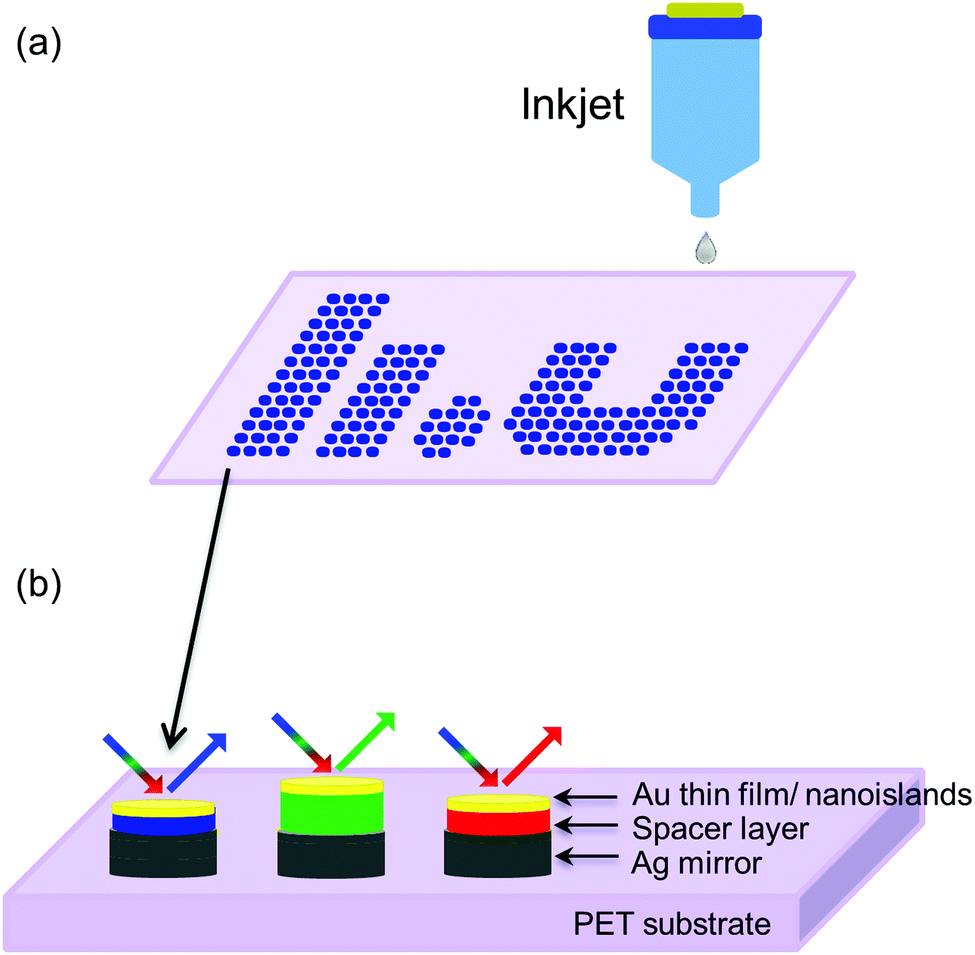 | ||
| Fig. 1 Structural colors by combination of Fabry–Pérot cavity and plasmonic metasurface. (a) Major fabrication steps are performed by inkjet printing. (b) Schematic illustration shows the different layers of the pixels (the colors of the spacer layers indicate different colors of the pixels, not the color of the spacer material itself). | ||
2. Results and discussion
We formed the bottom mirror of the pixels by inkjet-printing silver nanoparticles in squares onto flexible PET substrates, followed by annealing at 140 °C for 1 hour (Fig. S1a, ESI†). As expected, the silver layer with around 500 nm thickness is fully opaque and provides high reflection throughout the visible spectrum (Fig. S1c, ESI†). The reflection decreases somewhat towards the blue end of the spectrum, which we attribute to plasmonic absorption by silver nanoparticles remaining after annealing. Such nanoparticle features are indeed clearly visible in atomic force microscopy (AFM) images (see Fig. S1b, ESI†).Printing of the dielectric spacer layer is a crucial and challenging fabrication step, because color and cavity quality depend strongly on spacer thickness and uniformity. We use SU8 photoresist ink as a dielectric spacer, which provides high optical transparency throughout the visible range. Fig. 2a shows an optical photograph of SU8 pixels inkjet-printed using a standard SU8 ink and Fig. 2b and c present the AFM image of one of those pixels and height profile across the pixel, respectively. There is a clear non-uniformity across the pixels, with almost double thickness at the edge than that at the center. Such non-uniform thickness would be disadvantageous for our application by creating non-homogeneous reflected colors across single pixels. The ring phenomenon is known as the coffee ring or coffee stain effect, as first described by Deegan.45 During drying, the solvent evaporation rate at the edge of a droplet is greater than that at the center, as related to the edge being in contact with both air and substrate in a triple contact line.45–48 In turn, solvent lost by evaporation at the edge is replaced by solvent drawn from the center of the droplet, eventually depositing more solutes at the edge than at the center. The coffee ring effect forms a crucial issue also for other inkjet printing applications and substantial work has been performed to explore its mechanism and prevention.49–53 One solution to reduce the coffee ring effect is to introduce an inward recirculatory flow inside the droplet via the Marangoni effect, driven by surface-tension gradients produced by the latent heat of evaporation.49 We here adopt this approach by introducing a high-boiling point co-solvent to the SU8 ink. Cyclopentanone (boiling point = 130 °C) acts as the main solvent and we add the non-ionic surfactant Triton X-100 as the co-solvent (boiling point = 270 °C). Fig. 2d shows a photograph of pixels made from this co-solvent-based ink, indicating significantly more homogeneous pixels compared with those made from the initial ink. The corresponding AFM image (Fig. 2e) and height profile (Fig. 2f) indeed reveal highly uniform pixels without the coffee ring effect. The substantial improvement is related to the details of the drying mechanism of pixels made using both low and high-boiling point solvents. The higher solvent evaporation rate at the edge leads to an imbalance in mixture composition along the radius of the pixel. In turn, this imbalance induces a flow of the higher fraction of high-boiling point solvent towards the edge, which reduces the coffee stain effect and promotes homogeneous pixels.48 Notably, we found that the optimum ink formulation also depends on the substrate and we here optimized the conditions for the inkjet-printed silver mirror, while printing with the same ink on thermally evaporated silver showed strong coffee ring effect (Fig. S2, ESI†).
 | ||
| Fig. 2 Inkjet printing of SU8 photoresist as a transparent spacer layer on top of inkjet printed silver mirrors. (a) Microscopic image, (b) atomic force microscopic image, (c) height profile of the pixels printed with unmodified SU8 ink; (d) microscopic image, (e) atomic force microscopic image, (f) height profile of the pixels printed with ink modified by TX-100 as cosolvent; (g) variation of pixel thickness and diameter with solid content of the ink. The error bars correspond to the standard deviation. | ||
Control of spacer thickness is crucial for tuning the cavity resonance and color of the final pixels. We here investigate the possibility to control spacer thickness by varying the solid content of the ink while keeping the droplet volume constant. As shown in Fig. 2g (blue squares), the pixel spacer thickness increased monotonically from 56 nm to 156 nm when varying the solid content in the range from 10 wt% to 20 wt%, with a decreased coffee stain effect maintained. The pixel diameter did not vary much for the different inks and remained around 80–85 μm in the measured range of solid contents (black circles in Fig. 2g). Successful inkjet printing of pixels with uniform spacer layers with controlled thickness in the range of tens of nanometers to hundreds of nanometers shows promise for creating microcavities with structural coloration.
After optimizing uniformity and demonstrating thickness control of the spacer layer, we finalize the microcavity pixels by depositing a thin gold film (20 nm) as top layer. This semitransparent layer completes the optical microcavity, resulting in reflective colors that depend on spacer thickness (see Fig. S3, ESI†). The pixel color evolves from blue to red with increasing spacer layer thickness, in accordance with the corresponding increase in the optical path length of the microcavities. The gradual shift of the reflection dip is also clearly visible from the reflection spectra of the respective pixels (Fig. S3b, ESI†). The spectral features are relatively broad, which explains the lack of green reflected color during the gradual change in pixel thickness in this range. This feature may be due to some variation in thickness over the pixels. We also observe variation in color at the edge of the pixels, attributed to the non-perfect step function at the edges. Green structural coloration could instead be produced by thicker pixels. Fig. 3a–c show microcavity pixels with the three primary RGB colors, based on spacer layer thicknesses of approximately 67 nm (blue), 123 nm (red) and 300 nm (green) (Fig. 3a–c). Blue and red colors could be highly reproducible. It was more challenging to reproducibly print the higher spacer thickness for green pixels (300 nm) by only increasing the solid content of the ink. The green pixels in Fig. 3b therefore originate from certain regions with higher thickness obtained when printing with 18 wt% ink. These pixels show vibrant green coloration, which prompts for alternative approaches to reproducibly print pixels with higher spacer thicknesses. To address this issue, we investigated inkjet printing of two pixels at the same position, one on top of the other (with the 18 wt% ink). This enabled reproducible production of green pixels also, although with increased coffee ring effects (see Fig. S4, ESI†). Future work is needed to optimize inks and the printing procedure for double printed pixels.
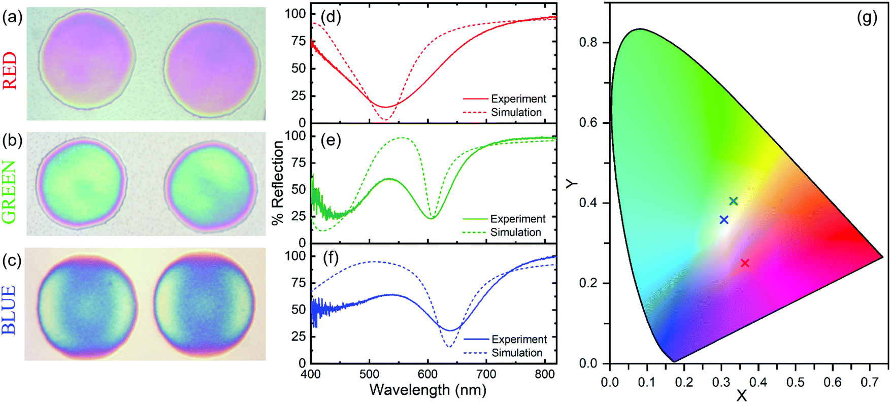 | ||
| Fig. 3 Red, green and blue (RGB) pixels based on Fabry–Pérot cavity having 20 nm thin gold film as the top layer. (a–c) Optical microscopy images of red (a), green (b) and blue (c) microcavity pixels; (d–f) reflection spectra of the corresponding RGB pixels, corresponding to spacer thicknesses of 123 nm (d), 300 nm (e), and 67 nm (f); solid and dashed lines represent experimental and simulated data, respectively; (g) CIE 1931 xy chromaticity space of the RGB pixels, marked by their respective colors. | ||
The reflection spectra obtained from the separate RGB pixels (solid lines in Fig. 3d–f) reveal more details of the cavity resonances and their contribution to the coloration. The red color (Fig. 3d) originates from a 1st order Fabry–Pérot resonance that significantly reduces the reflection in the blue and green wavelength regions. Some remaining blue reflection explains the non-negligible blue contribution to the color, as also clear from its position in the CIE 1931 xy diagram (Fig. 3g). The green color of the pixel with the highest thickness (300 nm) originates from a 2nd order cavity resonance, with reflection dips in both the blue and red spectral ranges (Fig. 3e). The zeroth order resonance of the blue pixel (Fig. 3f) provides a reflection spectrum that is similar to that of the green pixel, but with higher reflection in the blue region. However, the blue pixel also does not fully suppress green and red reflection, which is also evident from its position between the blue and green regions in the CIE diagram (Fig. 3g). The chromaticity of blue pixels could be improved by means to more efficiently absorb light in the green and red regions, which we investigate below. Simulated reflection spectra obtained using the finite-difference time-domain (FDTD) method reproduce all spectral features observed experimentally (dashed lines in Fig. 3d–f), albeit overall with more spectrally narrow features and more pronounced intensity variations. We attribute these deviations to differences between the experimental system and the more ideal simulated system. For example, the tendency of lower reflection in the blue region in the experiments agrees with the wavelength-dependent reflection of the inkjet-printed silver mirror (Fig. S1, ESI†).
As mentioned above, the blue pixels showed considerable reflection also in the green and red wavelength regions, positioning the color between blue and green in the CIE diagram (Fig. 3g). We therefore investigate the possibility to improve the chromaticity of the blue pixels using a semi-transparent top mirror that absorbs and scatters green and red light via plasmon excitation. Combined microcavity and plasmonic effects have previously shown the capability to provide metasurfaces with vibrant structural colors.23,24,54 In this work, we use discontinuous gold nanoisland films as a plasmonic semi-transparent top mirror, spontaneously formed by thermal evaporation of ultrathin layers of gold.55,56 The SEM images in Fig. 4a show the morphology of such gold films deposited on inkjet-printed pixels, in the thickness range from 5 nm to 20 nm. As the gold thickness decreases, the continuous film indeed starts to show discontinuities and the 5 nm thick layer shows an array of separated gold nanoislands of irregular shapes. In turn, the optical microscopy images in Fig. 4a show that the thinner gold films with nanoislands lead to significantly improved blue color. The corresponding reflection spectra of the different pixels (Fig. 4b) illustrate that the improved chromaticity is related to more efficient suppression of green and red reflection for pixels with plasmonic gold nanoislands compared with pixels with comparatively thicker continuous gold films. The results agree with suppressed reflection in the red and green regions due to plasmonic absorption and scattering by the gold nanoislands. Indeed, the extinction spectra of gold films on SU8 (no bottom mirror) display the formation of a broad plasmon resonance extinction peak around 750 nm for the 5 nm gold nanoisland film (Fig. S5, ESI†). Hence, the gold nanoislands in combination with the Fabry–Pérot cavity resonance enable ink-jet printed blue plasmonic microcavity pixels with very good chromaticity. In addition to plasmonic contribution, the gradual improvement in blue coloration with decreasing gold thickness may also be related to modifications in the direct reflection from the top mirror for different thicknesses. The evolution of the positions in the CIE diagram also illustrates the significant improvement in chromaticity for pixels with decreasing top gold thickness, with a consistent movement towards the blue region (see Fig. 4c). As expected, the chromaticity of the red pixels was not improved upon replacing the 20 nm gold mirror with the thin gold nanoisland films, but instead showed reduced color quality due to plasmon absorption in the red wavelength region (Fig. S6, ESI†). Similar strategies could, however, be applied for red pixels, but using plasmonic films with absorption in the blue and green regions. To demonstrate large-scale, easy and reproducible fabrication of plasmonic microcavity pixels with structural colors, we finally reproduced our blue university logo using the inkjet printing process, as shown in Fig. 4d. Further investigation shows that the pixels are highly stable, with no observable degradation either after storage under ambient conditions for around a year or after ultrasonication in water, isopropanol or acetone (see Fig. S7, ESI†).
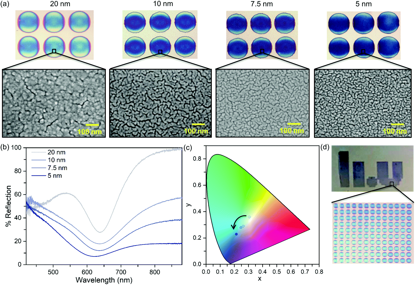 | ||
| Fig. 4 Enhanced color tunability by gold nanoislands as the top layer. (a) Optical microscopic images of the blue pixel with 20 nm, 10 nm, 7.5 nm and 5 nm ultrathin gold films as the top layer and the corresponding SEM images. (b) Reflection spectra in air at normal incidence from blue pixels with different top gold layers from thin films to nanoislands. (c) CIE 1931 xy chromaticity space of the blue pixels with a decrease in top layer thickness from 20 nm to 5 nm indicated by an arrow. (d) University logo printed in blue pixels. | ||
3. Conclusion
This study demonstrates scalable fabrication of structurally colored microcavities and plasmonic cavity pixels based on inkjet-printing. The simple three-step fabrication process includes a bottom silver mirror, a transparent spacer layer (SU8) and a semitransparent top layer that is either a continuous gold film or a plasmonic nanoisland film. We inkjet-printed large areas of the bottom silver mirror followed by printing of small (around 40 μm radius) pixels of the transparent spacer layer that were finally topped with the thin top layer by thermal evaporation. We found the detailed spacer ink-formulation to be essential for the quality of the pixels and the original ink led to highly non-uniform pixels with spatially varying thickness across each pixel. Adding a high boiling temperature co-solvent to the spacer ink solved this issue and enabled inkjet-printing of pixels with uniform thin dielectric spacer layers with minimal coffee ring effect. Varying the solid-ink content further allowed accurate control of pixel thickness in the range from around 50 to 150 nm. Clear pixel colors appeared after gold deposition, confirming the formation of microcavities with structural colors. We also found that replacing the top layer with a plasmonic gold nanoisland film could significantly improve the blue chromaticity, via localized plasmon absorption in the green and red wavelength regions. We demonstrated the concept of large-area fabrication by printing our blue university logo. To the best of our knowledge, this is the first report demonstrating fabrication of Fabry–Pérot cavities and plasmonic cavities by inkjet printing on non-patterned surfaces. The large-scale, simple and cheap production technology may be particularly suitable for applications such as reflective displays.Author contributions
M. P. J. proposed the initial idea and designed the project together with S. S. S. S. performed the device fabrication, characterization, simulations and data analysis. P. W. assisted in inkjet printing the silver mirror, E. S. H. K. performed SEM imaging and R. S. assisted in CIE plotting. S. S. and M. P. J. wrote the manuscript through contributions from all authors. All authors have given approval to the final version of the manuscript.Conflicts of interest
The authors declare no competing financial interest.Acknowledgements
We acknowledge financial support from the Swedish Foundation for Strategic Research, the ÅForsk Foundation, the Wenner-Gren Foundations, the Swedish Research Council, the Royal Swedish Academy of Sciences, and the Swedish Government Strategic Research Area in Materials Science on Functional Materials at Linköping University (Faculty Grant SFO-Mat-LiU No. 2009 00971).References
- A. Kristensen, J. K. W. Yang, S. I. Bozhevolnyi, S. Link, P. Nordlander, N. J. Halas and N. A. Mortensen, Nat. Rev. Mater., 2016, 2, 16088 CrossRef.
- K. Xiong, D. Tordera, M. P. Jonsson and A. B. Dahlin, Rep. Prog. Phys., 2019, 82, 024501 CrossRef PubMed.
- M. Keshavarz Hedayati and M. Elbahri, Plasmonics, 2017, 12, 1463–1479 CrossRef.
- Z. Li and Y. Yin, Adv. Mater., 2019, 31, 1807061 CrossRef PubMed.
- X. Du, T. Li, L. Li, Z. Zhang and T. Wu, J. Mater. Chem. C, 2015, 3, 3542–3546 RSC.
- M. Srinivasarao, Chem. Rev., 1999, 99, 1935–1962 CrossRef CAS PubMed.
- P. Vukusic and J. R. Sambles, Nature, 2003, 424, 852 CrossRef CAS PubMed.
- J. Huang, X. Wang and Z. L. Wang, Nano Lett., 2006, 6, 2325–2331 CrossRef CAS PubMed.
- A. R. Parker and H. E. Townley, Nat. Nanotechnol., 2007, 2, 347 CrossRef CAS PubMed.
- S. Kinoshita, S. Yoshioka and J. Miyazaki, Rep. Prog. Phys., 2008, 71, 076401 CrossRef.
- C. Lawrence, P. Vukusic and R. Sambles, Appl. Opt., 2002, 41, 437–441 CrossRef PubMed.
- Q. Zhao, Y. Wang, H. Cui and X. Du, J. Mater. Chem. C, 2019, 7, 6493–6511 RSC.
- K. Kumar, H. Duan, R. S. Hegde, S. C. W. Koh, J. N. Wei and J. K. W. Yang, Nat. Nanotechnol., 2012, 7, 557 CrossRef CAS PubMed.
- J. Olson, A. Manjavacas, T. Basu, D. Huang, A. E. Schlather, B. Zheng, N. J. Halas, P. Nordlander and S. Link, ACS Nano, 2016, 10, 1108–1117 CrossRef CAS PubMed.
- A. S. Roberts, A. Pors, O. Albrektsen and S. I. Bozhevolnyi, Nano Lett., 2014, 14, 783–787 CrossRef CAS PubMed.
- J. Hao, R. Mohamad, A. Mahssa and K. Bozena, Nano Futures, 2017, 1, 025001 CrossRef.
- M. Miyata, H. Hatada and J. Takahara, Nano Lett., 2016, 16, 3166–3172 CrossRef CAS PubMed.
- T. H. Chen and B. M. Reinhard, Adv. Mater., 2016, 28, 3522 CrossRef CAS PubMed.
- S. J. Tan, L. Zhang, D. Zhu, X. M. Goh, Y. M. Wang, K. Kumar, C.-W. Qiu and J. K. W. Yang, Nano Lett., 2014, 14, 4023–4029 CrossRef CAS PubMed.
- J. Xue, Z.-K. Zhou, Z. Wei, R. Su, J. Lai, J. Li, C. Li, T. Zhang and X.-H. Wang, Nat. Commun., 2015, 6, 8906 CrossRef CAS PubMed.
- X. Zhu, C. Vannahme, E. Højlund-Nielsen, N. A. Mortensen and A. Kristensen, Nat. Nanotechnol., 2015, 11, 325 CrossRef PubMed.
- Y. Gu, L. Zhang, J. K. W. Yang, S. P. Yeo and C.-W. Qiu, Nanoscale, 2015, 7, 6409–6419 RSC.
- K. L. Xiong, G. Emilsson, A. Maziz, X. X. Yang, L. Shao, E. W. H. Jager and A. B. Dahlin, Adv. Mater., 2016, 28, 9956–9960 CrossRef CAS PubMed.
- K. Xiong, D. Tordera, G. Emilsson, O. Olsson, U. Linderhed, M. P. Jonsson and A. B. Dahlin, Nano Lett., 2017, 17, 7033–7039 CrossRef CAS PubMed.
- T. Xu, E. C. Walter, A. Agrawal, C. Bohn, J. Velmurugan, W. Zhu, H. J. Lezec and A. A. Talin, Nat. Commun., 2016, 7, 10479 CrossRef CAS PubMed.
- Y.-K. R. Wu, A. E. Hollowell, C. Zhang and L. J. Guo, Sci. Rep., 2013, 3, 1194 CrossRef PubMed.
- X. M. Goh, Y. Zheng, S. J. Tan, L. Zhang, K. Kumar, C.-W. Qiu and J. K. W. Yang, Nat. Commun., 2014, 5, 5361 CrossRef CAS PubMed.
- T. Ellenbogen, K. Seo and K. B. Crozier, Nano Lett., 2012, 12, 1026–1031 CrossRef CAS PubMed.
- B. Zeng, Y. Gao and F. J. Bartoli, Sci. Rep., 2013, 3, 2840 CrossRef PubMed.
- S. Yokogawa, S. P. Burgos and H. A. Atwater, Nano Lett., 2012, 12, 4349–4354 CrossRef CAS PubMed.
- B. D. Lucas, J.-S. Kim, C. Chin and L. J. Guo, Adv. Mater., 2008, 20, 1129–1134 CrossRef CAS.
- C. Yindar, L. Clint, O. Badr, H. Donna, V. G. Sasan, K. Karen and K. Bozena, Nanotechnology, 2013, 24, 055304 CrossRef PubMed.
- P. Zijlstra, J. W. M. Chon and M. Gu, Nature, 2009, 459, 410 CrossRef CAS PubMed.
- L. Cui, Y. Li, J. Wang, E. Tian, X. Zhang, Y. Zhang, Y. Song and L. Jiang, J. Mater. Chem., 2009, 19, 5499–5502 CAS.
- L. Bai, Z. Xie, W. Wang, C. Yuan, Y. Zhao, Z. Mu, Q. Zhong and Z. Gu, ACS Nano, 2014, 8, 11094–11100 CrossRef CAS PubMed.
- S. Wu, B. Liu, X. Su and S. Zhang, J. Phys. Chem. Lett., 2017, 8, 2835–2841 CrossRef CAS PubMed.
- M. Kuang, J. Wang, B. Bao, F. Li, L. Wang, L. Jiang and Y. Song, Adv. Opt. Mater., 2014, 2, 34–38 CrossRef.
- H. Nam, K. Song, D. Ha and T. Kim, Sci. Rep., 2016, 6, 30885 CrossRef CAS PubMed.
- J. Hou, M. Li and Y. Song, Angew. Chem., Int. Ed., 2018, 57, 2544–2553 CrossRef CAS PubMed.
- Y. Huang, W. Li, M. Qin, H. Zhou, X. Zhang, F. Li and Y. Song, Small, 2017, 13, 1503339 CrossRef PubMed.
- A. V. Yakovlev, V. A. Milichko, V. V. Vinogradov and A. V. Vinogradov, ACS Nano, 2016, 10, 3078–3086 CrossRef CAS PubMed.
- A. V. Yakovlev, V. A. Milichko, V. V. Vinogradov and A. V. Vinogradov, Adv. Funct. Mater., 2015, 25, 7375–7380 CrossRef CAS.
- H. Jiang, S. Alan, H. Shahbazbegian, J. N. Patel and B. Kaminska, ACS Nano, 2016, 10, 10544–10554 CrossRef CAS PubMed.
- H. Jiang and B. Kaminska, ACS Nano, 2018, 12, 3112–3125 CrossRef CAS PubMed.
- R. D. Deegan, O. Bakajin, T. F. Dupont, G. Huber, S. R. Nagel and T. A. Witten, Nature, 1997, 389, 827 CrossRef CAS.
- M. Anyfantakis and D. Baigl, Angew. Chem., Int. Ed., 2014, 53, 14077–14081 CrossRef CAS PubMed.
- D. Kim, S. Jeong, B. K. Park and J. Moon, Appl. Phys. Lett., 2006, 89, 264101 CrossRef.
- M. Robin, W. Kuai, M. Amela-Cortes, S. Cordier, Y. Molard, T. Mohammed-Brahim, E. Jacques and M. Harnois, ACS Appl. Mater. Interfaces, 2015, 7, 21975–21984 CrossRef CAS PubMed.
- H. Hu and R. G. Larson, J. Phys. Chem. B, 2006, 110, 7090–7094 CrossRef CAS PubMed.
- J. Park and J. Moon, Langmuir, 2006, 22, 3506–3513 CrossRef CAS PubMed.
- C. Seo, D. Jang, J. Chae and S. Shin, Sci. Rep., 2017, 7, 500 CrossRef PubMed.
- P. He and B. Derby, Adv. Mater. Interfaces, 2017, 4, 1700944 CrossRef.
- D. Soltman and V. Subramanian, Langmuir, 2008, 24, 2224–2231 CrossRef CAS PubMed.
- A. M. Shaltout, J. Kim, A. Boltasseva, V. M. Shalaev and A. V. Kildishev, Nat. Commun., 2018, 9, 2673 CrossRef PubMed.
- G. Kalyuzhny, A. Vaskevich, M. A. Schneeweiss and I. Rubinstein, Chem. – Eur. J., 2002, 8, 3849–3857 CrossRef CAS.
- I. Doron-Mor, H. Cohen, Z. Barkay, A. Shanzer, A. Vaskevich and I. Rubinstein, Chem. – Eur. J., 2005, 11, 5555–5562 CrossRef CAS PubMed.
Footnote |
| † Electronic supplementary information (ESI) available: Materials and methods. Characterization of inkjet printed silver mirrors. Role of surface roughness of the bottom mirror in printing the spacer layer. Systematic study of the effect of spacer layer thickness on color. Extinction spectra of the gold nanoislands. Role of thin film and nanoislands as a top layer for red pixels. Stability of the pixels. See DOI: 10.1039/c9tc02796c |
| This journal is © The Royal Society of Chemistry 2019 |