Locking excitons in two-dimensional emitting layers for efficient monochrome and white organic light-emitting diodes†
Received
23rd May 2019
, Accepted 24th June 2019
First published on 24th June 2019
Abstract
Simplified organic light-emitting diodes (OLEDs) with high efficiency are key for successful products. Here, we demonstrate simplified OLEDs by combining ultra-thin non-doped emitting layers (UN-EMLs) with charge-transfer (CT)-type mixed donor–acceptor recombination layers. The CT recombination layers provide a bipolar recombination zone and improved long-range coupled Förster energy transfer. The UN-EMLs not only remain similar in optical properties compared to the doped-EMLs including photoluminescence quantum yield and emitter orientation but also mitigate charge trapping by the emitters in the CT-host systems despite the large energy level differences. The results of time-resolved photoluminescence decay reveal that although a five times smaller volume emitter is used in the UN-EMLs, the intensity of triplet–triplet annihilation stays comparably low by restricting the exciton migration to the two-dimensional plane. Making use of the excellent optoelectronic properties of the proposed system, green OLEDs with extremely simplified structures reach an external quantum efficiency (EQE) of 23.2%, nicely matching with the optical simulation results. Furthermore, white OLEDs with the same structure achieve a maximum EQE of 18.7% with considerably low efficiency roll-off. The combined system demonstrated here provides a novel approach for significantly simplified and tunable device structures of OLEDs, while maintaining high performance.
Introduction
Organic light-emitting diodes (OLEDs) are one of the most elegant demonstrations of plastic electronic devices.1–3 Allowing ultra-thin, scalable, flexible, and high color quality devices, OLEDs are revolutionizing displays and light-emitting panels. On the way to realizing highly efficient devices competitive with inorganic counterparts, a major breakthrough for OLEDs was the introduction of the “triplet harvesting concept” into the emitting layer by phosphorescent4 and thermally activated delayed fluorescent (TADF) emitters.5 Conventionally, the emitters are diluted into matrix materials to avoid intermolecular interactions and concentration quenching, which results in a low photoluminescence quantum yield (PLQY) with a redshifted and broadened emission spectrum.6 Therefore, the harmony between the host material and the emitter plays a crucial role in developing efficient and stable OLEDs.7 In terms of host materials, many compounds were designed, including unipolar, bipolar and mixed host materials, pursuing the goal of high and balanced bipolar mobility, good thermal stability, and sufficient triplet energy for exciton confinement.8,9 Recently, two types of charge-transfer (CT) host systems based on either inter- or intramolecular CT states have emerged as efficient hosts for blue, green, red and even infra-red OLEDs, with bipolar and low energy loss between the hosts and emitters.10,11 Moreover, the triplet excitons can be thermally activated to singlet states in the CT-hosts, promoting Förster energy transfer and extending the triplet harvesting radius.12,13 Without the need of new synthesis, the former charge-transfer system, which is referred to as the ‘exciplex’ system in the field of OLEDs,14 consisting of a p-type material and an n-type material, has been reported to reach efficiencies for monochrome phosphorescent and TADF emitters that are close to the theoretical limit while showing a low efficiency roll-off.15–17 Unfortunately, a universal CT-host system for various emitters remains inaccessible due to the considerable energy level difference between host materials (donor and acceptor) and different emitters. Commonly, the doping ratio of phosphorescent and TADF emitters varies from 5–20%, corresponding to a density of 1019–1020 cm−3. Such high density makes the charge trapping by the emitter become a vital intermediate in the charge transport and recombination process.18 This often leads to the confinement of charges and excitons to very small volumes. In OLEDs, the emitter typically captures only one type of charge, resulting in charge imbalance and a shift of the recombination zone under different driving voltages.19–21 This bottleneck limits the use of a single CT-host system in white OLEDs. Instead, many sophisticated device structures have been developed for white OLEDs, increasing the complexity for physical modelling and sacrificing the potential for commercialization.22–25
For the simplification of the device architecture, undoped emitting layers are used as an alternative. For example, non-doped Pt-complex, TADF and aggregation-induced emission (AIE) based blue OLEDs are reported with an EQE of 31%, 19.5% and 3.99%, respectively.26–28 To make this strategy universal for phosphorescent emitters, an ultra-thin non-doped emitting layer (UN-EML) was proposed.29,30 Recently, various device structures consisting of UN-EMLs were reported for monochrome and white OLEDs, reaching efficiency values similar to those of doped EMLs.31–35 Further, the UN-EML concept can be combined with doped phosphorescent, charge-transfer (‘exciplex’) and TADF EMLs for simplified and efficient white OLEDs.36,37 Despite the rapid development and decent efficiency of the UN-EML based devices, the optical properties of the UN-EML, the recombination process and the origin of the low efficiency roll-off of these devices, which are imperative for the future rational design of efficient devices, still remain unclear.
Here, we present simplified monochrome and white OLEDs integrating UN-EMLs and CT-type mixed donor–acceptor recombination layers. We comparatively investigate UN-EMLs with their doped counterparts of two Ir-complex emitters bis(2-phenylpyridine)iridium acetylacetonate (Ir(ppy)2(acac)) and bis(2-methyldibenzo[f,h]quinoxaline)(acetylacetonate)iridium(III) (Ir(MDQ)2(acac)). A comprehensive analysis of the optical properties reveals that the UN-EMLs show a similar photoluminescence (PL) spectrum, PLQY and emitter orientation with respect to the doped EMLs, implying that molecular aggregation, which would be detrimental for the performance, is negligible. The photoluminescence decay measurements indicate that the UN-EMLs are beneficial for triplet–triplet annihilation (TTA) suppression, suggesting a comparably low efficiency roll-off despite the five times smaller volume of the emitters. Using a CT system as the recombination layers, green and red OLEDs reach a maximum external quantum efficiency (EQE) of 23.2% and 17.2%, respectively. The EQE remains very high at high current densities: the characteristic current densities, where the EQE is reduced to half of its initial value, are 246 mA cm−2 and 230 mA cm−2 for the green and red OLEDs, respectively. By investigating the charge recombination processes in the emitting layers, it is revealed that the ultra-thin body of the UN-EMLs also effectively mitigates direct trapping of charges by emitter molecules. This allows designing the emitting layer with more flexibility as the exciton formation can be spatially broadened compared to conventional doped EMLs. Furthermore, a white OLED is designed with the same device structure, realizing a maximum EQE of 18.7%. The configuration of OLEDs demonstrated here provides a great opportunity to significantly simplify the device structure for monochrome and white OLEDs while maintaining high performance.
Results and discussion
Optical properties of the UN-EML
Doped EMLs have been developed mainly to avoid detrimental effects at high concentrations such as aggregation, quenching of the exciton and changes in the emitter orientation. Such systems can be considered as a good reference system for studying alternative EML concepts. Here, the optical properties of doped EMLs and UN-EMLs are comparatively studied to understand the possible limitations of the latter. The results are summarized in Table 1. The PL spectra of red and green UN-EML with peaks at 520 nm and 612 nm with a full width at half maximum (FWHM) of 66.8 nm and 88.6 nm, respectively, are shown in Fig. S1, ESI.† These values are consistent with the corresponding doped EMLs. Red shifts or spectrum broadening, which are indicative of emitter aggregation,38 are not observed. As shown in Fig. S2–S5 (ESI†), the PLQY values of the green and red doped EMLs are 87.6 ± 0.1%, 77.8 ± 0.1%, respectively. In comparison, the PLQY values for the green and red UN-EMLs of 88.2 ± 0.8% and 76.0 ± 0.8%, respectively, are virtually identical. We also comparatively studied the orientation of the emitters, as shown in Fig. S6 (ESI†). The green and red doped EMLs show anisotropy coefficients of 0.28 ± 0.02 and 0.24 ± 0.03, while the green and red UN-EMLs yield values of 0.27 ± 0.02 and 0.28 ± 0.03, respectively. Here, the emitter molecules in the red UN-EML seem to have a slightly weaker tendency to orient horizontally compared to those in the doped EML. The cause for this difference is not understood. In summary, the optical measurements demonstrate that the doped and non-doped emitting layers perform very similarly.
Table 1 Summary of the optical properties of UN-EMLs and doped EMLs
| Emitter |
Emission peak [nm] |
FWHM [nm] |
PLQY [%] |
Orientation |
| Green UN-EML |
520 |
66.8 |
88.2 ± 0.8 |
0.27 ± 0.02 |
| Green doped EML |
521 |
67.8 |
87.6 ± 0.1 |
0.28 ± 0.02 |
| Red UN-EML |
612 |
88.6 |
76.0 ± 0.8 |
0.28 ± 0.03 |
| Red doped EML |
611 |
89.9 |
77.8 ± 0.1 |
0.24 ± 0.03 |
As shown in Fig. S7 (ESI†), roughly a 0.1 nm sub monolayer reaches 10 mol% by treating all molecules as nanoballs with 1 nm diameter and assuming only 1 nm is needed to form a continuous film. Moreover, the deposited organic layer has a general roughness of 0.1–1 nm,39 which can lead to an even lower doping concentration. Considering the amount of emitter molecules in a certain thickness, the UN-EML discussed here has several times fewer emitter molecules compared to the doped EML of the same thickness. For example, for the red emitter, a 30 nm 10 wt% doped EML has around 3 nm pure emitters whereas the UN-EML only has 0.6 nm emitters with the same total thickness. To reach the same luminance, the exciton density in these UN-EMLs needs to be approximately 5 times higher than that in the doped EMLs, raising a concern about serious triplet–triplet annihilation (TTA), which significantly limits the high brightness performance of phosphorescent and TADF OLEDs. The TTA process is strongly dependent on the exciton density. In time-resolved PL experiments, increasing exciton density makes the transient PL data deviate from a monoexponential law caused by significant bimolecular contributions. Considering this bimolecular TTA, the exciton decay can be modelled as:40
| | 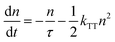 | (1) |
Here,
n is the triplet exciton density,
τ is the triplet exciton lifetime, and
kTT is the TTA rate constant. By solving
eqn (1), the time evolution of the exciton density in the film after a short laser pulse is given by:
| | 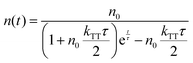 | (2) |
with the initial triplet exciton density
n0. To clarify the TTA process in the UN-EML, we measure the time-resolved PL decay at different exciton densities. A structure of 3 nm mCP
![[thin space (1/6-em)]](https://www.rsc.org/images/entities/char_2009.gif)
:
B3PYMPM (1
:
1 by weight)/[0.1 nm emitter/5 nm mCP
:
B3PYMPM (1
:
1)]
5/0.1 nm emitter/3 nm mCP
:
B3PYMPM (1
:
1) is adopted for the UN-EML and 50 nm doped EML is utilized as the reference.
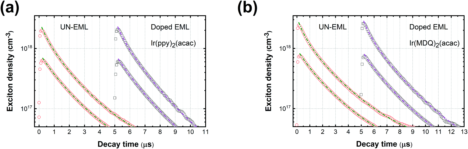
Fig. 1a and b show the PL decay curves of the UN-EMLs compared to doped EMLs at high and low pump levels. Taking the ultra-thin body of the UN-EML into account, there are two extreme cases in estimating the actual exciton density: one is that the excitons are distributed homogenously throughout the whole organic layer and the other is that the excited excitons are transferred from the CT-host system to the UN-EMLs immediately after generation, which results in a relatively high exciton concentration within the UN-EML planes. In the first case, both UN-EMLs and doped EMLs reach comparable pump levels,
i.e. around 0.8 ± 0.3 × 10
17 and 2.5 ± 1.0 × 10
18 cm
−3 for low and high pump levels, respectively, which are estimated from the laser power energy and absorption spectrum of the thin film.
41–43 The exciton lifetime
τ is derived from the long tail of the PL decay curve and
kTT is set as the fit parameter. The dashed lines in
Fig. 1 show the calculated fits according to
eqn (2). All the decay curves fit well with the TTA model. Table S1 (ESI
†) shows the parameters determined from the time-resolved PL curves. Both green and red emitters show a similar triplet exciton lifetime (around 1.60 ± 0.10 μs for Ir(ppy)
2(acac) and 2.13 ± 0.19 μs for Ir(MDQ)
2(acac)). The green control sample Ir(ppy)
2(acac) realizes a
kTT of 0.8 ± 0.3 × 10
−12 cm
3 s
−1 and 0.6 ± 0.2 × 10
−12 cm
3 s
−1 and the red control sample Ir(MDQ)
2(acac) shows a
kTT of 0.8 ± 0.3 × 10
−12 cm
3 s
−1 and 0.5 ± 0.2 × 10
−12 cm
3 s
−1 for the low and high pump levels, respectively. The rate constant of Ir(ppy)
2(acac) agrees well with the earlier reported
kTT.
38 The
kTT value of the UN-EMLs is very similar to the doped one. For instance, at a high pump level, Ir(ppy)
2(acac) and Ir(MDQ)
2(acac) UN-EMLs show a
kTT of 0.7 ± 0.3 × 10
−12 cm
3 s
−1 and 0.6 ± 0.2 × 10
−12 cm
3 s
−1, respectively, which is only slightly higher than that of the control samples. If, however, the exciton transfer from the CT-host system to the emitter is much faster than the decay of the exciton on the emitter, we consider the second case. The corresponding exciton density of the UN-EMLs is 5.3 times higher than that of the first case, resulting in an extremely low
kTT of 0.2 ± 0.1 × 10
−12 cm
3 s
−1 and 0.1 ± 0.1 × 10
−12 cm
3 s
−1 at low and high pump levels, respectively, as shown in Table S1 (ESI
†). Because exciton diffusion and transfer are not instantaneous, they take some time, and the real exciton density and
kTT of the UN-EMLs, which cannot be determined based on the data available, should be between these two extreme cases. The reason for the low
kTT of UN-EMLs is shown in Fig. S8 (ESI
†). After the excitons are captured by the emitters, the TTA process takes place by exciton migration between the emitters.
42 In a conventional doped EML, exciton diffusion can randomly occur in each direction. In the UN-EML, the exciton migration in the direction perpendicular to the substrate is suppressed due to the ultrathin body of the emitting layer and the high triplet energy of both donor and acceptor materials of the CT-host system, restricting the exciton diffusion to occurring only in two-dimensional planes. This reduces the probability of the excitons moving towards each other, which is a prerequisite for TTA
via Dexter transfer. The trade-off between high exciton concentration and suppression of exciton diffusion makes the UN-EML achieve comparable PL decay characteristics, which suggests the efficiency roll-off of the corresponding OLEDs to be similar to the conventional doped EML.
 |
| | Fig. 1 (a) PL decay curves of Ir(ppy)2(acac) in the form of UN-EML and doped EML under high and low pump levels, respectively; (b) PL decay curves of Ir(MDQ)2(acac) of the UN-EML and doped EML under high and low pump levels, respectively. The dashed lines show the calculated fits according to rate eqn (2). | |
Monochrome OLEDs
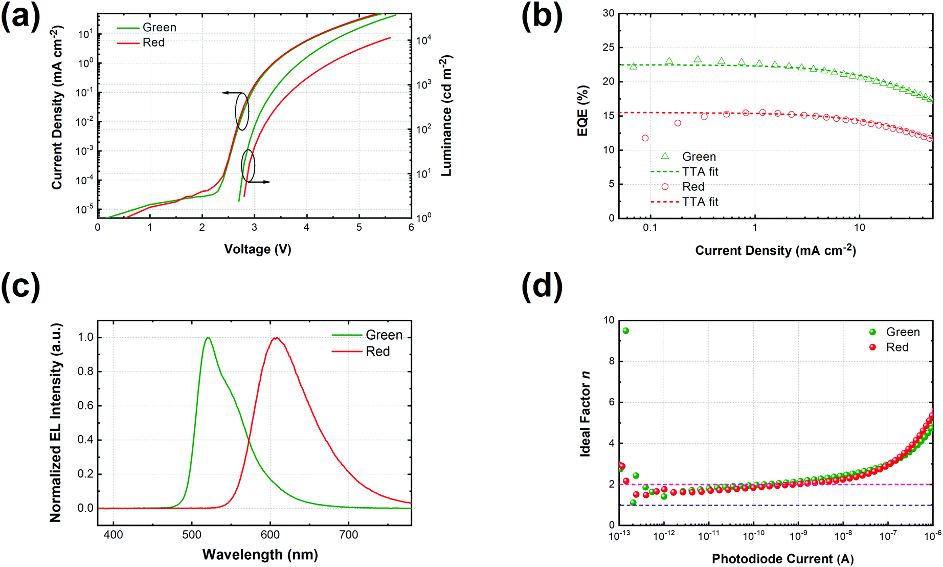
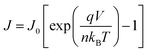
Fig. 2 shows the device structure of the monochrome OLEDs. For simplicity, 5 nm mCP:(25 wt%) MoO3 and 5 nm Bphen:Cs (1:1) are used as hole injection and electron injection layers, respectively. 45 nm mCP and 50 nm B3PYMPM are utilized as hole and electron transport layers, respectively. For the emitting layer, a 10 nm CT-host blend of mCP:B3PYMPM (1:1) is used as the recombination layer. Three 0.1 nm UN-EMLs are inserted between the CT-host recombination layers with an equal spacing of 5 nm. Both the singlet and triplet exciton diffusion lengths are larger than 2.5 nm.44,45 Moreover, the conversion from triplet to singlet in the CT system enhances the long-range coupled Förster transfer.12,13 Thus, the 5 nm space ensures that all the excitons independent of their spin generated in the recombination layer can be harvested by the emitters, either by Förster resonance energy transfer or Dexter exchange energy transfer. The bipolar character of the CT-host material system is beneficial to dilute the exciton density and subsequently reduces the efficiency roll-off. The triplet energy of B3PYMPM, mCP and the mixed film of mCP:B3PYMPM are 2.68 eV, 2.90 eV and 2.97 eV,15 respectively, ensuring efficient triplet confinement and suppressing the energy transfer between the individual UN-EMLs. Fig. 3a shows the J–V–L characteristics of the monochrome OLEDs. The green and red OLEDs share exactly the same electrical performance, indicating that a similar recombination process takes place in the devices. The devices show a low voltage of 2.98 V and 3.13 V at 100 cd m−2 for the green and red OLEDs, respectively. The EQE versus current density of these two devices is plotted in Fig. 3b. The green and red OLEDs reach a maximum EQE of 23.2% and 15.6%, respectively. At a luminance of 1000 cd m−2, the EQE still remains at high values of 22.5% and 15.0% for the green and red OLEDs, respectively, indicating a low efficiency roll-off. To quantify this roll-off, the TTA model is used to fit the efficiency roll-off characteristics of the devices, which is given by:40| |  | (3) |
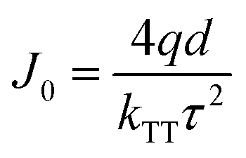
Here, η0 is the maximum EQE without the TTA process and J0 is the critical current density where ηEQE = 50% η0 and it follows:| |  | (4) |
where q is the elementary charge and d is the thickness of the exciton recombination zone. For simplicity, possible triplet-polaron quenching processes are not considered in this analysis.41 Thus, it is important to note that the derived rate constants from the EQE fit may contain such contributions, rendering kTT an effective rate constant in this case. A critical current density of 246 mA cm−2 and 230 mA cm−2 is realized for the green and red OLEDs, respectively. Assuming a homogeneous exciton distribution in the 10 nm charge recombination layers (first extreme case) and taking the average exciton lifetime from the PL decay measurements into account, i.e. τ = 1.68 μs and τ = 2.23 μs, the TTA rate constant kTT from such fits is determined to be 0.9 × 10⁻¹² cm3 s−1 and 0.6 × 10⁻¹² cm3 s−1 for the green and red OLEDs, respectively. For the second extreme case, the TTA rate constant kTT is determined to be 0.27 × 10⁻¹² cm3 s−1 and 0.18 × 10⁻¹² cm3 s−1 for the green and red OLEDs, respectively. These values are similar to the time-resolved PL decay measurement, inferring that the TTA strongly dominates the efficiency roll-off process.
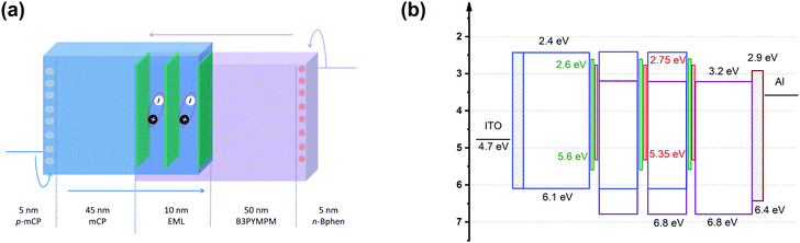 |
| | Fig. 2 (a) Device architecture for monochrome OLEDs. Three UN-EMLs (0.1 nm) are spaced by 5 nm mCP:B3PYMPM (1:1), which is adopted as a charge recombination layer. The triplet energy of B3PYMPM, mCP and the CT-host blend of mCP:B3PYMPM is 2.68, 2.90 and 2.97 eV, respectively, ensuring efficient triplet confinement.15 (b) Energy level diagram of the materials used for the device. The highest occupied molecular orbital (HOMO) differences for mCP and Ir(ppy)2(acac) and mCP and Ir(MDQ)2(acac) are 0.5 eV and 0.75 eV, respectively.3,15 | |
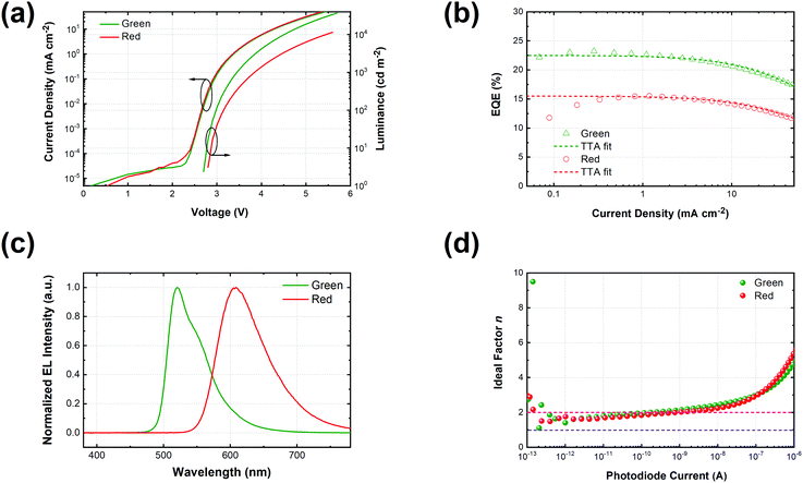 |
| | Fig. 3 (a) Current density–voltage–luminance curves of green and red monochrome OLEDs based on the same device architecture; (b) EQE along with the current density of green (triangle) and red (circles) OLEDs together with fitting curves based on the TTA model (dashed line); (c) normalized electroluminescent spectra of red and green OLEDs at 15.4 mA cm−2; (d) the ideality factor (n) of luminance (photodiode current)–voltage curves calculated according to eqn (6). | |
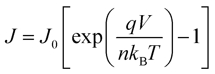
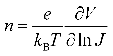
Fig. 3c shows the normalized electroluminescence spectra at 15.4 mA cm−2. Both of them show pure emission from the emitters, peaking at 520 nm and 609 nm without residual emission from the CT-host blend, indicating that the excitons are completely captured by the emitters. In addition, Fig. S9 (ESI†) shows the emission spectra of the devices at different current densities, varying from 1.55 mA cm−2 to 31.01 mA cm−2. The spectra of both devices remain unchanged. To understand how exciton generation takes place in the devices, a high-resolution luminance–voltage (L–V) measurement is carried out. The Shockley diode equation is adopted for the diffusion dominated region, which reads:46
| |  | (5) |
where
J0 is the saturation reverse dark current,
q is the elementary charge,
n is the ideality factor,
kB is the Boltzmann constant and
T is the temperature. The ideality factor
n could be extracted as:
| |  | (6) |
The ideality factor
n is a fingerprint to differentiate between Langevin recombination and trap assisted Shockley–Read–Hall (SRH) recombination, which would yield a value of 1 and 2, respectively.
47–49 As shown in
Fig. 3d, both devices reach an ideality factor of 1.61 for the luminance–voltage curves at a temperature of 300 K. This suggests that Langevin recombination exists in both devices even at very low current density. However, the SRH recombination could not be excluded though the ideality factor of unity is hardly reached due to the series resistance of the transport layers.
48,50 This will be discussed further in the study on white OLEDs, which confirms that SRH recombination also contributes to parts of the exciton generation.
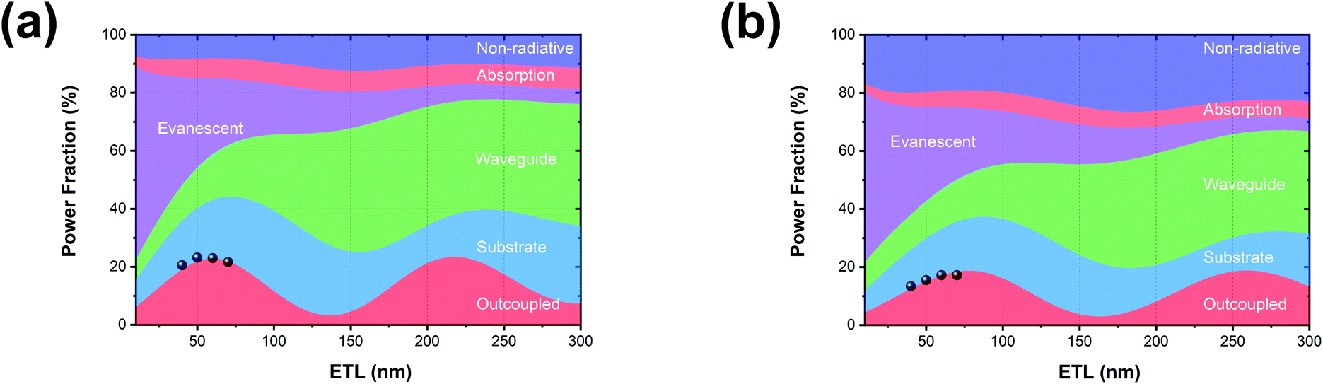
Simulation of monochrome OLEDs
Based on the optical properties of the UN-EMLs, we simulate the power dissipation of the devices as a function of electron transport layer thickness by using the classic dipole model and assuming the recombination rate to be unity. As shown in Fig. 4a and b, the maximum predicted theoretical value of the outcoupled modes reaches 22.9% and 18.7% for green and red monochrome OLEDs, respectively. Accounting for the substrate mode, which could be extracted by external outcoupling techniques such as half sphere and texture structure, the green and red OLEDs could reach EQEs of 44.2% and 37.3%, respectively. To experimentally verify the simulation results, we fabricated the green and red devices with an electron transport layer thickness of 40–70 nm. All the device performance data are shown in Fig. S10 and S11 (ESI†) in the supporting information. The maximum EQEs of these devices are shown in Fig. 4, agreeing well with the simulation results. The green and red monochrome OLEDs reach maximum EQEs of 23.2% and 17.2% in the experiment, respectively. These experimental EQE values are very close to the optical simulation, suggesting that the electrical loss in non-doped OLEDs is negligible.
 |
| | Fig. 4 Optical simulation results as a function of electron transport layer (ETL) thickness of (a) green (Ir(ppy)2(acac)) and (b) red (Ir(MDQ)2(acac)) OLEDs. The black dots in (a) and (b) are the experimental results for different ETL thicknesses. | |
White OLEDs
Based on the highly efficient monochrome OLEDs, white OLEDs are designed with the structure shown in Fig. 5a. The basic device structure is the same as for the monochrome OLEDs. A blue phosphorescent emitter bis[2-(4,6-difluorophenyl)pyridinato-C2,N](picolinato)iridium(III) (FIrpic) is utilized for the blue emission color. 0.1 nm Ir(ppy)2(acac), Ir(MDQ)2(acac) and FIrpic are equally separated by 5 nm CT-host recombination layers each. For the optimization of the white spectrum, two mixing ratios (mCP:B3PYMPM: W1 = 1:1 and W2 = 3:7) of the CT-host are used. As shown in Fig. 5c, W1 shows a maximum EQE of 18.7% with a CIE of (0.44, 0.49) and a CRI of 74 at 15.4 mA cm−2. W2 shows a maximum EQE of 14.2% and a CIE of (0.50, 0.43) and a CRI of 81 at 15.4 mA cm−2, reaching candle-light-style warm white light (Fig. S12, ESI†).51 Devices W1 and W2 also show very low efficiency roll-off, reaching a critical current density of 329 mA cm−2 and 299 mA cm−2 according to eqn (3), respectively. The EQE of W1 and W2 remains at 18.6% and 14.1% at 1000 cd m−2, and 17.9% and 13.1% at 5000 cd m−2, respectively. Fig. 5d shows the spectra of device W2 at different current densities. Device W2 shows very good color stability over a wide current density range of 1.5–23.1 mA cm−2, corresponding to a luminance of 319–4673 cd m−2. To clarify the origin for the good color stability, a W3 device is designed with a switched position of the red and blue emitters. As shown in Fig. 5e, the spectrum of W3 shifts remarkably at different current densities. It can be inferred that the trapping through emitter molecules still exists there and cannot be ignored in the design of white OLEDs being quite sensitive to the changes in the recombination zone (cf.Fig. 5f). Considering the Langevin recombination process found in the monochrome OLEDs, the recombination in the white OLEDs must be a combination of Langevin and SRH recombination processes. Nevertheless, due to the ultra-thin body of the UN-EMLs and a small amount of emitter, the trapping of emitter molecules is still lowered to a degree, allowing excitons to spread over the whole EML for sufficient green emission in W1.
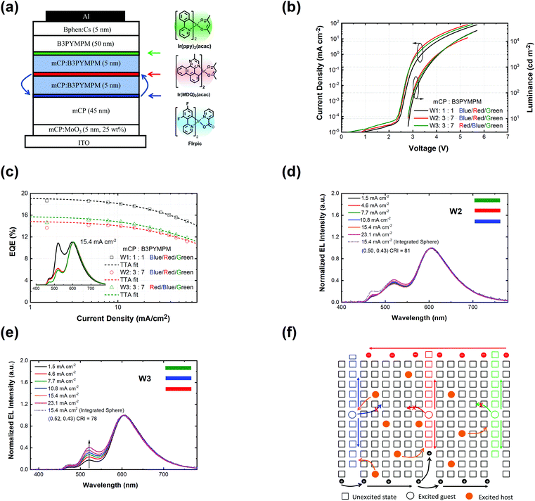 |
| | Fig. 5 (a) Device structure for white OLEDs. The order of emitter is blue/red/green for W1, blue/red/green for W2, red/blue/green for W3. The mixing ratio of mCP:B3PYMPM is 1:1, 3:7 and 3:7 for W1, W2 and W3, respectively; (b) current density–voltage–luminance curves of white OLEDs; (c) EQE as a function of current density of white OLEDs. The dashed lines are the fitting curves based on the TTA model with a critical current density of 329, 299 and 269 mA cm−2 for W1, W2 and W3, respectively. The inset shows the electroluminescence spectra at 15.40 mA cm−2 of these three devices; (d) electroluminescence spectra along with current densities of W2; (e) electroluminescence spectra along with current densities of W3; (f) charge recombination and exciton transfer processes of white OLEDs. | |
Conclusions
In this study, we present a novel and highly promising approach for OLEDs using ultrathin non-doped emitting layers with charge-transfer-type recombination layers. The ultra-thin non-doped emitting layers not only possess similar optical properties compared to doped emitting layers such as photoluminescence quantum yield and emitter orientation but also benefit the electrical properties, i.e. mitigating direct trapping of charges by emitter molecules. Upon restricting the exciton diffusion to a two-dimensional grid, the ultrathin non-doped emitting layers reach a comparable low triplet–triplet annihilation rate to the doped emitting layers, although the volume of the emitters is around 5 times smaller than that of the doped ones. In combination with the bipolar and improved long-range coupled Förster energy transfer properties of the charge-transfer host, a green OLED with an extremely simplified structure achieves a maximum EQE of 23.2%, nicely matching with the optical simulation results. Furthermore, a white OLED is designed with the same device structure, achieving a maximum efficiency of 18.7% with considerably low efficiency roll-off. The device strategy proposed here may shed light on the design of more efficient highly simplified OLEDs and show great potential for mass production.
Experimental section
Fabrication and characterization of OLEDs
The organic materials were sublimated at least twice before evaporation. The devices are deposited on commercial glass patterned with an ITO electrode. Before deposition, the substrates were cleaned with acetone, ethanol and deionized water and treated by UV-ozone. The deposition process was entirely completed in an ultra-high-vacuum chamber (Kurt J. Lesker Co.) with a base pressure of 10−8 mbar. The deposition rate, film thickness and doping concentration were monitored in situ by quartz crystal monitors. The deposition rate is 0.3–0.5 Å s−1 for the organic material and 2 Å s−1 for Al. After deposition, the devices were encapsulated by glass lids and UV-glue under a nitrogen atmosphere. The electrical and optical characteristics of the devices were measured using an automatic home-made system containing a calibrated spectrometer (Instrument Systems GmbH CAS140CT), a Keithley 2400 SourceMeter and a silicon photodiode. The EQE of the devices was measured by using an integrating sphere (Labsphere LMS-100). The EQE of the white OLEDs was calibrated according to the spectrum changes at different current densities. The high-resolution luminescence–voltage curves were measured by using a Keithley 2602 and 2635 SourceMeter and a silicon photodiode.
Photophysical measurements of the UN-EML
The structure of the UN-EMLs for photophysical measurements is quartz/3 nm mCP:B3PYMPM (1:1)/[0.1 nm emitter/5 nm mCP:B3PYMPM (1:1)]5/0.1 nm emitter/3 nm mCP:B3PYMPM (1:1). The control samples are quartz/50 nm mCP:B3PYMPM:emitter (1:1, 8 wt% for green and 10 wt% for red emitter, respectively). The PL spectrum was measured using a spectrofluorometer (Spex FluoroMax). The PLQY was obtained using an integrated sphere together with a CAS 140 CT spectrometer and a 340 nm excitation source (Thorlabs M340L4). The PLQY results were corrected by considering the reabsorption of the samples. The angular resolved photoluminescence was measured by using an Ocean Optics USB 4000 spectrometer together with a rotational stage. A polarization filter was placed before the spectrometer for removing the transverse electric component of the emission. The time-resolved photoluminescence spectrum was measured using a pulsed nitrogen laser (MNL 200 Lasertechnik Berlin) operating at 337 nm with a pulse duration of 1.3 ns and a fast Si-photodetector (PDA100A-EC, Thorlabs). The signal was read out by using an oscilloscope. A mask was used to control the excitation size and the exciton density was calculated using a power meter according to a procedure we earlier reported elsewhere.41
Simulation of the devices
For OLED optical mode simulation, we utilized a classical electromagnetic model. The radiative dipole was treated as the electrical dipole antenna and the transfer matrix method was used for calculations. The detailed simulation process was described by Furno et al.52 All the materials used in the device simulation are treated as isotropic, except the emitters. The refractive index of the used materials is shown in Fig. S13 (ESI†). The emission spectrum, PLQY and emitter orientation were obtained from the experimental measurements and the exciton generation rate was set to unity.
Conflicts of interest
There are no conflicts to declare.
Acknowledgements
Y. Liu is grateful for the financial support from the China Scholarship Council (No. 201506920047). Z. W. is grateful for the funding from the Alexander von Humboldt-Foundation. This work received funding from the European Research Council under the European Union's Horizon 2020 research and innovation programme (Grant Agreement No. 679213; project acronym BILUM). We also thank Dr Axel Fischer for fruitful and critical discussion.
References
- C. W. Tang and S. A. VanSlyke, Appl. Phys. Lett., 1987, 51, 913–915 CrossRef CAS.
- S. R. Forrest, Nature, 2004, 428, 911–918 CrossRef CAS PubMed.
- S. Reineke, F. Lindner, G. Schwartz, N. Seidler, K. Walzer, B. Lussem and K. Leo, Nature, 2009, 459, 234–238 CrossRef CAS PubMed.
- M. A. Baldo, D. F. O'Brien, Y. You, A. Shoustikov, S. Sibley, M. E. Thompson and S. R. Forrest, Nature, 1998, 395, 151–154 CrossRef CAS.
- H. Uoyama, K. Goushi, K. Shizu, H. Nomura and C. Adachi, Nature, 2012, 492, 234–238 CrossRef CAS PubMed.
- Y. Kawamura, K. Goushi, J. Brooks, J. J. Brown, H. Sasabe and C. Adachi, Appl. Phys. Lett., 2005, 86, 071104 CrossRef.
- D. Zhang, M. Cai, Y. Zhang, D. Zhang and L. Duan, Mater. Horiz., 2016, 3, 145–151 RSC.
- Y. Tao, C. Yang and J. Qin, Chem. Soc. Rev., 2011, 40, 2943–2970 RSC.
- A. Chaskar, H.-F. Chen and K.-T. Wong, Adv. Mater., 2011, 23, 3876–3895 CrossRef CAS PubMed.
- M. Y. Wong and E. Zysman-Colman, Adv. Mater., 2017, 29, 1605444 CrossRef PubMed.
- M. Sarma and K.-T. Wong, ACS Appl. Mater. Interfaces, 2018, 10, 19279–19304 CrossRef CAS PubMed.
- Y.-K. Wang, S.-H. Li, S.-F. Wu, C.-C. Huang, S. Kumar, Z.-Q. Jiang, M.-K. Fung and L.-S. Liao, Adv. Funct. Mater., 2018, 28, 1706228 CrossRef.
- H. Wang, L. Meng, X. Shen, X. Wei, X. Zheng, X. Lv, Y. Yi, Y. Wang and P. Wang, Adv. Mater., 2015, 27, 4041–4047 CrossRef CAS PubMed.
- S. Ullbrich, J. Benduhn, X. Jia, V. C. Nikolis, K. Tvingstedt, F. Piersimoni, S. Roland, Y. Liu, J. Wu, A. Fischer, D. Neher, S. Reineke, D. Spoltore and K. Vandewal, Nat. Mater., 2019, 18, 459–464 CrossRef CAS PubMed.
- H. Shin, S. Lee, K.-H. Kim, C.-K. Moon, S.-J. Yoo, J.-H. Lee and J.-J. Kim, Adv. Mater., 2014, 26, 4730–4734 CrossRef CAS PubMed.
- J. W. Sun, J.-H. Lee, C.-K. Moon, K.-H. Kim, H. Shin and J.-J. Kim, Adv. Mater., 2014, 26, 5684–5688 CrossRef CAS PubMed.
- Y. Seino, S. Inomata, H. Sasabe, Y.-J. Pu and J. Kido, Adv. Mater., 2016, 28, 2638–2643 CrossRef CAS PubMed.
- M. L. Tietze, P. Pahner, K. Schmidt, K. Leo and B. Lüssem, Adv. Funct. Mater., 2015, 25, 2701–2707 CrossRef CAS.
- Z. Wu, J. Luo, N. Sun, L. Zhu, H. Sun, L. Yu, D. Yang, X. Qiao, J. Chen, C. Yang and D. Ma, Adv. Funct. Mater., 2016, 26, 3306–3313 CrossRef CAS.
- Y. Liu, L.-S. Cui, M.-F. Xu, X.-B. Shi, D.-Y. Zhou, Z.-K. Wang, Z.-Q. Jiang and L.-S. Liao, J. Mater. Chem. C, 2014, 2, 2488–2495 RSC.
- Y. Liu, B. Nell, K. Ortstein, Z. Wu, Y. Karpov, T. Beryozkina, S. Lenk, A. Kiriy, K. Leo and S. Reineke, ACS Appl. Mater. Interfaces, 2019, 11, 11660–11666 CrossRef CAS PubMed.
- S.-F. Wu, S.-H. Li, Y.-K. Wang, C.-C. Huang, Q. Sun, J.-J. Liang, L.-S. Liao and M.-K. Fung, Adv. Funct. Mater., 2017, 27, 1701314 CrossRef.
- Z. Wu, L. Yu, F. Zhao, X. Qiao, J. Chen, F. Ni, C. Yang, T. Ahamad, S. M. Alshehri and D. Ma, Adv. Opt. Mater., 2017, 5, 1700415 CrossRef.
- S. Jeon, S. Lee, K.-H. Han, H. Shin, K.-H. Kim, J.-H. Jeong and J.-J. Kim, Adv. Opt. Mater., 2018, 6, 1701349 CrossRef.
- Y. Liu, F. Liang, L.-S. Cui, X.-B. Shi, Z.-K. Wang and L.-S. Liao, Adv. Opt. Mater., 2016, 4, 2051–2056 CrossRef CAS.
- Q. Wang, I. W. Oswald, X. Yang, G. Zhou, H. Jia, Q. Qiao, Y. Chen, J. Hoshikawa-Halbert and B. E. Gnade, Adv. Mater., 2014, 26, 8107–8113 CrossRef CAS PubMed.
- Q. Zhang, B. Li, S. Huang, H. Nomura, H. Tanaka and C. Adachi, Nat. Photonics, 2014, 8, 326 CrossRef CAS.
- J. Huang, N. Sun, J. Yang, R. Tang, Q. Li, D. Ma and Z. Li, Adv. Funct. Mater., 2014, 24, 7645–7654 CrossRef CAS.
- T. Tsuji, S. Naka, H. Okada and H. Onnagawa, Appl. Phys. Lett., 2002, 81, 3329–3331 CrossRef CAS.
- Z. Su, W. Li, M. Xu, T. Li, D. Wang, W. Su, J. Niu, H. He, J. Zhu and B. Chu, J. Phys. D: Appl. Phys., 2007, 40, 2783–2786 CrossRef CAS.
- Y. Zhao, J. Chen and D. Ma, ACS Appl. Mater. Interfaces, 2013, 5, 965–971 CrossRef CAS PubMed.
- B. Liu, H. Tao, L. Wang, D. Gao, W. Liu, J. Zou, M. Xu, H. Ning, J. Peng and Y. Cao, Nano Energy, 2016, 26, 26–36 CrossRef CAS.
- S.-H. Li, S.-F. Wu, Y.-K. Wang, J.-J. Liang, Q. Sun, C.-C. Huang, J.-C. Wu, L.-S. Liao and M.-K. Fung, J. Mater. Chem. C, 2018, 6, 342–349 RSC.
- Y. Miao, K. Wang, B. Zhao, L. Gao, P. Tao, X. Liu, Y. Hao, H. Wang, B. Xu and F. Zhu, Nanophotonics, 2018, 7, 295–304 CAS.
- Y. Miao, K. Wang, L. Gao, H. Wang, F. Zhu and B. Xu, J. Mater. Chem. C, 2018, 6, 9811–9820 RSC.
- J. Wang, J. Chen, X. Qiao, S. M. Alshehri, T. Ahamad and D. Ma, ACS Appl. Mater. Interfaces, 2016, 8, 10093–10097 CrossRef CAS PubMed.
- S. Ying, J. Yao, Y. Chen and D. Ma, J. Mater. Chem. C, 2018, 6, 7070–7076 RSC.
- S. Reineke, T. C. Rosenow, B. Lüssem and K. Leo, Adv. Mater., 2010, 22, 3189–3193 CrossRef CAS PubMed.
- T. W. Lee, T. Noh, H. W. Shin, O. Kwon, J. J. Park, B. K. Choi, M. S. Kim, D. W. Shin and Y. R. Kim, Adv. Funct. Mater., 2009, 19, 1625–1630 CrossRef CAS.
- M. A. Baldo, C. Adachi and S. R. Forrest, Phys. Rev. B: Condens. Matter Mater. Phys., 2000, 62, 10967–10977 CrossRef CAS.
- S. Reineke, K. Walzer and K. Leo, Phys. Rev. B: Condens. Matter Mater. Phys., 2007, 75, 125328 CrossRef.
- S. Reineke, G. Schwartz, K. Walzer and K. Leo, Appl. Phys. Lett., 2007, 91, 123508 CrossRef.
- S. Reineke, G. Schwartz, K. Walzer, M. Falke and K. J. A. P. L. Leo, Appl. Phys. Lett., 2009, 94, 116 CrossRef.
- J. Wünsche, S. Reineke, B. Lüssem and K. Leo, Phys. Rev. B: Condens. Matter Mater. Phys., 2010, 81, 245201 CrossRef.
- S. Hofmann, T. C. Rosenow, M. C. Gather, B. Lüssem and K. Leo, Phys. Rev. B: Condens. Matter Mater. Phys., 2012, 85, 245209 CrossRef.
- M. Kuik, G.-J. A. H. Wetzelaer, H. T. Nicolai, N. I. Craciun, D. M. De Leeuw and P. W. M. Blom, Adv. Mater., 2014, 26, 512–531 CrossRef CAS PubMed.
- A. Fischer, M. Pfalz, K. Vandewal, S. Lenk, M. Liero, A. Glitzky and S. Reineke, Phys. Rev. Appl., 2018, 10, 014023 CrossRef CAS.
- J. Wu, A. Fischer and S. Reineke, Adv. Opt. Mater., 2019, 0, 1801426 CrossRef.
- J.-H. Lee, S. Lee, S.-J. Yoo, K.-H. Kim and J.-J. Kim, Adv. Funct. Mater., 2014, 24, 4681–4688 CrossRef CAS.
- W. Song, J. Y. Lee, Y. J. Cho, H. Yu, H. Aziz and K. M. Lee, Adv. Sci., 2018, 5, 1700608 CrossRef PubMed.
- J.-H. Jou, C.-Y. Hsieh, J.-R. Tseng, S.-H. Peng, Y.-C. Jou, J. H. Hong, S.-M. Shen, M.-C. Tang, P.-C. Chen and C.-H. Lin, Adv. Funct. Mater., 2013, 23, 2750–2757 CrossRef CAS.
- M. Furno, R. Meerheim, S. Hofmann, B. Lüssem and K. Leo, Phys. Rev. B: Condens. Matter Mater. Phys., 2012, 85, 115205 CrossRef.
Footnote |
| † Electronic supplementary information (ESI) available. See DOI: 10.1039/c9tc02768h |
|
| This journal is © The Royal Society of Chemistry 2019 |
Click here to see how this site uses Cookies. View our privacy policy here. 
 Open Access Article
 This Open Access Article is licensed under a
  ,
Jinhan
Wu
,
Simone
Lenk
,
Karl
Leo
and
Sebastian
Reineke
,
Jinhan
Wu
,
Simone
Lenk
,
Karl
Leo
and
Sebastian
Reineke