
 Open Access Article
 This Open Access Article is licensed under a Creative Commons Attribution-Non Commercial 3.0 Unported Licence
Fabrication of SnS nanowalls via pulsed plasma-enhanced chemical vapor deposition using a metal–organic single-source precursor†
Charlotte
Ruhmlieb
 *a,
Young Joo
Lee
b,
Christian
Strelow
a,
Tobias
Kipp
a and
Alf
Mews
a
*a,
Young Joo
Lee
b,
Christian
Strelow
a,
Tobias
Kipp
a and
Alf
Mews
a
aUniversity of Hamburg, Institute of Physical Chemistry, Grindelallee 117, 20146 Hamburg, Germany. E-mail: charlotte.ruhmlieb@chemie.uni-hamburg.de
bUniversity of Hamburg, Institute of Applied and Inorganic Chemistry, Martin-Luther-King-Platz 6, 20146 Hamburg, Germany
First published on 26th July 2019
Abstract
Orthorhombic tin(II)sulfide (α-SnS) is a IV–VI p-type semiconductor that is characterized by its layered crystal structure, resulting in a two-dimensional anisotropic crystal growth. The according interlayer gaps feature an enhanced electron mobility, compared to the charge mobility perpendicular to the growth direction. Consequently, when SnS is electrically contacted, light-generated charge carriers can be rapidly separated and transported along the interlayer gaps, so that charge-carrier recombination is minimized. This anisotropic electric transport might be utilized to improve the performance of optoelectronic devices, e.g., solar cells, when the absorbing layer consists of vertically aligned crystalline SnS nanowalls, following the vertical working geometry of the device. We report on the plasma-enhanced chemical vapor deposition (PECVD) of accurately aligned, highly crystalline SnS nanowalls on metal-covered wafer substrates. Our approach contains the thermal evaporation of a solid single-source precursor, mainly bis(diethyldithiocarbamato)tin(II), that is characterized in depth via, e.g., solid-state 119Sn-NMR spectroscopy. In situ optical emission spectroscopy of the plasma indicates the plasma-induced decomposition of the precursor. At an elevated substrate temperature of 400 °C, predominantly vertically oriented stacks of phase-pure SnS are grown, while at a low substrate temperature of 250 °C, very thin SnS nanowalls are formed, if the used wafer was covered with steel/18Cr/9Ni. Electric measurements of the SnS nanowalls indicate an enhanced conductivity in comparison to stacked SnS.
1 Introduction
The discovery of single-layered graphite, i.e., graphene, and the related groundbreaking investigations paved the way for extensive research on two-dimensional nanostructures and their applications. The spatial limitation of a semiconductor to the scale where its charge carriers are confined can significantly change its physical and chemical properties. The crystalline texture of layered structures is made up of stacked layers. Charge carriers are confined in the gap between these layers and can only move along two dimensions.1 The group of layered metal (di)chalcogenides comprises such van der Waals structures, e.g., MoS2 and WS2.2 Another highly noted material is orthorhombic tin(II)sulfide (α-SnS), which is composed of layered SnS sheets with the lone pair electrons directed into the interlayer space.3 Tian and coworkers investigated the in-plane anisotropic charge transport in α-SnS, as predicted by Xin et al., and identified the [001] direction to be dominant for electron movement.4,5 Since the direct bandgap of SnS (1.3 eV)6 hits the theoretical efficiency maximum for single-junction solar cells, the intrinsic p-type SnS is a highly promising absorber material for photovoltaics.7,8 Tin sulfide is a non-toxic, earth-abundant and chemically stable material with a strong optical absorption (>104 cm−1)9 and a proper carrier concentration.10 A long lifetime of photo generated charge carriers has been reported, which is eligible for efficient photovoltaics.11 Hence, SnS should be an appropriate alternative to CdTe, for instance, but until now, the highest efficiency for SnS-based solar cells does not exceed 5%.12 A non-optimized device fabrication and intrinsic material limitations, i.e., structural defects, are regarded as responsible for the low efficiency.10 Researches on thin-film fabrication of crystalline α-SnS have been striving, in order to minimize structural defects that influence the electrical performance. One commonly known technique is the deposition of a thin tin layer with subsequent sulfurization at high-vacuum conditions, as reported by Yang and coworkers for the fabrication of SnSx films.13 Miles et al. directly evaporated pure SnS powder and obtained a smooth tin-sulfide layer with a thickness of a few micrometers on glass substrates.14 Depending on the substrate temperature, additional phases of SnS2 or Sn2S3 appeared. The implementation of SnS layers from thermal evaporation of pure SnS into a highly complex, well-tuned solar-cell design led to efficiencies in the range of 1.1% to 2.6%.15 Beside traditional physical vapor deposition techniques, other related methods like electrodeposition16,17 and sputtering6,18 were applied for SnS deposition.An alternative approach for thin-film fabrication is chemical vapor deposition (CVD), which offers an extended range of parameters, e.g., reactants, and improved reaction control. Mutlu and coworkers reported on a straightforward CVD method for producing SnS2 nanostructures.19 Sulfur and tin dioxide were co-evaporated at high temperatures (T = 710 °C) within an evacuated quartz tube, leading to the formation of a SnS2-sheet network on a nearby substrate. Aerosol-assisted chemical vapor deposition (AACVD) allows for much milder evaporation conditions, since liquid precursor solutions can be used. The precursor is suspended in a liquid–gas system (aerosol) and is pyrolyzed into a solid product. Parkin et al. applied AACVD for SnS synthesis by using an aerosol of Sn(SCH2CH2S)2 in acetone.20 The resulting tin oxides were sulfurized in presence of H2S. Ramasamy and coworkers performed AACVD of SnS nanostructures without external sulfur supply by using diorganotin dithiocarbamates in toluene as precursors.21 Similarly, Kevin et al. used bis(dialkyldithiocarbamato)tin(II) complexes in tetrahydrofuran for AACVD of SnS.22 Ahmet and coworkers demonstrated polymorph-selective AACVD of SnS by using (dimethylamido)(N-phenyl-N′,N′-dimethylthiouriate)tin(II) dimer.23 Also chemical bath deposition was used for the fabrication of SnS nanowalls. For this, a mixture constituted of tin chloride hydrate, acetone, triethanolamine, thioacetamide, ammonia solution, and distilled water was used, as described in ref. 24.
A very elegant way for the formation of SnS was achieved by using organotin complexes as single-source precursors for the formation of SnS without generating aerosols. Park et al. performed metal–organic chemical vapor deposition (MOCVD) for SnS fabrication by using bis(3-mercapto-1-propanethiolato)tin(II) as precursor.25
Besides phase- and composition control, another important parameter for the possible application of tin-sulfide nanostructures is the control of morphology. In the particular case of SnS, ideally thin SnS nanosheets are grown perpendicular to the substrate and form so-called nanowalls. Photo generated charge carriers could then be directly transported along the fast channel in the interlayer gap. Moreover, nanowalls feature an extraordinary high surface-to-volume ratio that offers a large reactive surface area. A very prominent example for nanowalls are carbon nanowalls.26,27 These structures are typically synthesized via plasma-enhanced chemical vapor deposition (PECVD). In the past, PECVD has already been used for the deposition of tin sulfide. Ortiz and coworkers fed a capacitively-coupled radio frequency (RF) plasma with H2S, SnCl4, and hydrogen gas for 10 min.28 At a substrate temperature higher than 200 °C, the deposited material was phase-pure SnS. High plasma power led to a preferential growth along [111] direction. Depending on the flow rates, and thus precursor concentration, the composition of the resulting SnxSy phase was influenced.29 Cheng et al. used the PECVD technique to fabricate SnS2 nanoflowers and nanowalls.30 For this, sulfur or Na2S2O3·5H2O and SnCl4·5H2O were used as solid-source materials, which were separately evaporated before reaching the RF plasma. The morphology and crystallinity of the deposited SnS2 was influenced by substrate material and substrate temperature.31 The co-evaporation of Na2S2O3·5H2O and SnCl2·2H2O, instead of SnCl4·5H2O, led to the formation of SnS via PECVD.32 The preferential orientations of the deposited SnS on silicon and glass were identified to be (111), respectively, and (120) on fluorine-doped tin oxide.
In this work, we report on the large-area deposition of accurately aligned SnS nanowalls via PECVD technique using the solid metal–organic single-source precursor bis(diethyldithiocarbamato)tin(II). We present an extensive study on the structure and thermal supply of the precursor, including 119Sn magic angle spinning (MAS) NMR spectroscopy. Optical emission spectroscopy indicates the plasma-induced decomposition of the precursor. We also demonstrate the crucial parameters on influencing the morphology of the PECVD-grown SnS structures and work out criteria for vertical SnS growth. Finally, we show first results on the electrical characterization of the structures by I–V curve measurements, proving the drastically enhanced conductivity of the very thin, highly crystalline nanowalls.
2 Results and discussion
2.1 Precursor
One of the crucial requirements for a controlled PECVD of crystalline nanostructures is the usage of an appropriate precursor, which is ideally a non-toxic, stable and easy-to-prepare substance. For the synthesis of tin-sulfide nanowalls, we decided to use the tin-organic compound bis(N,N-diethyldithiocarbamato)tin(II) ([Sn(dedtc)2]) as a single-source precursor. The advantage of using a single-source precursor is that a precise timing to keep the concentrations of the reactants on point, which is required for a co-evaporation method of multiple precursors, can be avoided. [Sn(dedtc)2] can be synthesized by dropwise addition of diethylamine in ice-cold carbon disulfide under inert conditions, followed by adding a solution of SnCl2 in absolute ethanol.33 Bratspies and coworkers similarly mixed the diethylammonium salt of diethyldithiocarbamic acid with tin(II)chloride in ethanolic solution.34 Alternatively, [Sn(dedtc)2] can be easily prepared via co-precipitation reaction of tin dichloride with sodium N,N-diethyldithiocarbamate trihydrate in polar solvents.22,35,36 Elsewhere, inert conditions are recommended.37 In order to keep the entire nanowall-fabrication procedure as simple as possible, we prepared the tin-organic precursor via a precipitation reaction of SnCl2·2H2O with Na(dedtc)·3H2O in water. After vacuum drying over two days, the resulting yellow powder was stored under nitrogen atmosphere to avoid subsequent oxidation.The powder has been investigated with regard to elemental composition, molecular and crystalline structure, and thermal decomposition behavior. Powder X-ray diffraction indicates a micro-crystalline condition of the precursor powder (see Fig. S1, ESI†). Via energy-dispersive X-ray spectroscopy (EDX) an overall elemental composition of C10.2N2.2O1.1S3.3Sn1.0 was determined, indicating a slight deviation from the ideal elemental composition of pure Sn(dedtc)2. Solid-state 119Sn-NMR spectroscopy is an appropriate method to characterize the tin-organic precursor, due to its sensitivity to the local environment of the tin nucleus. The 119Sn MAS NMR spectrum of the precursor, acquired by Hahn-echo pulse sequence, shows four distinct signals at −565, −608, −695 and −737 ppm, indicating that the precursor consists of several species (Fig. 1a, top spectrum). To distinguish between organic and inorganic tin compounds, a 119Sn{1H} cross-polarization (CP) MAS NMR experiment was performed since the signals of the tin nucleus nearby protons (organotin or tin hydroxide) can be selectively enhanced by CP technique, which is based on the polarization transfer from protons to the observed nucleus. Three signals at −565, −695 and −737 ppm are still observed, whereas the signal at −608 ppm is not present (Fig. 1a, second from top), suggesting that this signal results from an inorganic tin species containing no protons. A 119Sn-NMR signal at −603 ppm with relatively small anisotropy has been reported for SnO2,38 which is similar to our observation. Thus, we assign the broad signal at −608 ppm to amorphous SnO2. In order to identify the remaining tin-organic compounds, we performed selective crystallization of the precursor powder. From a saturated solution of the precursor in acetone we received single crystals of tetrakis(N,N-diethyldithiocarbamato)tin(IV) ([Sn(dedtc)4]), while the crystallization from methanol led to the formation of μ-disulfido-bis(bis(N,N-diethyldithiocarbamato)tin(II)) ([S2Sn2(dedtc)4]) single crystals. Finely crushed powders of the single crystals were investigated via119Sn MAS NMR spectroscopy, respectively. As shown in Fig. 1(a), for [S2Sn2(dedtc)4] a signal at −738 ppm was measured and for [Sn(dedtc)4] a signal at −696 ppm was recorded. These signals coincide with the signals at −695 ppm and −737 ppm in the original spectrum. Consequently, we assign the signals at −695 ppm and −737 ppm in the original spectrum to [Sn(dedtc)4] and [S2Sn2(dedtc)4], respectively. This result is also confirmed by the NMR studies of Barone and coworkers.39 Finally, following ref. 40, the remaining peak at −565 ppm in the original spectrum can be attributed to [Sn(dedtc)2]. Here, the observed intense spinning sideband manifold with large anisotropy agrees with the asymmetric coordination environment of [Sn(dedtc)2] and thus confirms this assignment. Moreover, we performed 119Sn MAS NMR spectroscopy of the precipitation product of the reaction of SnCl2·2H2O and Na(dedtc)·3H2O in methanol instead of water (see Fig. 1(a), bottom). We identified this powder to be pure Sn(dedtc)2, since only one signal occurs at −565 ppm showing intense spinning side bands, indicating an asymmetric environment of the tin nucleus. 119Sn MAS NMR spectroscopy allows not only for the identification of the tin compounds, but also gives an estimation of the quantitative composition of the precursor powder. From the intensity distribution of the peaks (including spinning sidebands) in the original NMR spectrum we find that [Sn(dedtc)2] is the main compound with approx. 50 mol%, SnO2 represents approx. 38 mol%, [Sn(dedtc)4] amounts to approx. 10 mol%, and [S2Sn2(dedtc)4] contributes approx. 2 mol% to the precursor. All identified tin-organic compounds contain both product elements, i.e., tin and sulfur, and no co-evaporation of reactants takes place, hence the terminology of a single-source precursor is appropriate.
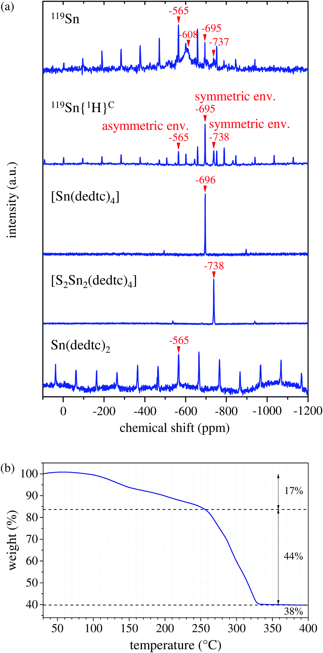 | ||
| Fig. 1 (a) 119Sn MAS NMR spectrum and 119Sn{1H} CP MAS NMR spectrum of the precursor in comparison to 119Sn MAS NMR spectra of tetrakis(diethyldithiocarbamato)tin(IV), sulfur-bridged dimeric Sn(dedtc)2 single-crystal powders and Sn(dedtc)2. NMR spectra of the precursor, Sn(dedtc)2, and single-crystalline compounds were acquired at spinning frequencies of 14, 15, and 30 kHz, respectively. The isotropic signals are marked with arrows. The other signals are spinning sidebands. The spectra are vertically shifted for clarity. (b) Thermogravimetric data of the used precursor heated in argon atmosphere at normal pressure with a heating rate of 5 °C min−1. | ||
Since the powdery precursor is thermally evaporated during the PECVD of tin-sulfide nanowalls, the thermal behavior of the precursor has been examined via TGA in argon atmosphere at normal pressure. The data is shown in Fig. 1(b) and is intended to give a first impression on the properties of the precursor upon thermal treatment. The TGA curve can be divided into three sections. First, a weight loss of approx. 17% can be detected from 100 °C to 250 °C, followed by a one-step drop of 44% from ca. 250 °C to ca. 320 °C. A residual amount of 38% remains at temperatures up to 400 °C. Interestingly, this is in good agreement with the quantification from the 119Sn-NMR spectroscopy, when the relative molar ratios are translated into mass percentages: 6 w% [S2Sn2(dedtc)4], 55 w% [Sn(dedtc)2], 15 w% SnO2, and 24 w% [Sn(dedtc)4]. In this case, the drop of 44% at ca. 250 °C could therefore be related to the evaporation of the main compound [Sn(dedtc)2]. Since the 119Sn NMR data identified [Sn(dedtc)2] to be the main compound of the precursor powder, this component primarily determinates the thermal characteristic of the precursor powder. As described by Bratspies et al.,34 at normal pressure [Sn(dedtc)2] melts at approx. 108 °C and shows decomposition at a temperature range between 210 °C and 360 °C. This is in total agreement with our TGA data, shown in Fig. 1(b), confirming that the major component of the precursor powder is indeed [Sn(dedtc)2] consistent with the NMR results. The deviation of 40 °C in decomposition temperature might be due to mixing effects among the compounds in the precursor powder, e.g., melting or boiling point elevations. Here it should be noted that the TGA measurements were carried out in argon atmosphere at normal pressure, while for the PECVD a vacuum of 1.9 mbar is used. Although the heating rate of ca. 5 °C min−1 is equivalent to the heating rate used in the PECVD, the TGA data is not fully comparable to the evaporation behavior of the precursor at vacuum condition. At normal pressure we also observe melting of the yellow precursor powder with color change to dark orange accompanied by gas formation. During the PECVD at low pressure, on the other hand, no significant melting or color change can be observed. Instead, at approx. 230 °C the precursor powder just vaporizes or seems to sublimate. A similar difference in thermal behavior under different pressure is described in ref. 34: at atmospheric nitrogen pressure, [Sn(dedtc)2] melts at 106 °C, followed by decomposition at 210–360 °C with residue formation, whereas at low pressure [Sn(dedtc)2] melts at 108 °C and then vaporizes at 150–250 °C with only very small residue.
In order to further investigate the precursor evaporation at vacuum condition, optical emission spectroscopy during the PECVD process was performed.
2.2 Optical emission spectroscopy
In order to get a more detailed insight into the plasma processes upon precursor vaporization, we performed optical emission spectroscopy (OES) of the plasma before and during the PECVD of SnS. Since nitrogen plasma typically shows broad comb-like emission lines over a broad range of the spectrum, we focused on the optical region with less nitrogen signals between 380 and 650 nm wavelength. In Fig. 2(a), the optical emission spectra of the Ar/N2 plasma before the precursor evaporation (black) and during the SnS deposition (red) are shown. A thorough comparison of both spectra reveals that additional emission lines occur during the precursor evaporation (highlighted with grey background). Actually, most of these lines can be assigned to atomic and molecular fragments of the precursor. In particular, sulfur lines are visible at 545.3, 555.9, 560.7, and 569.1 nm (SII), while the signals at 398.5 nm and 617.1 nm can be related to SnII and SnI species, respectively, indicating that tin and sulfur are set free by plasma impact. The signals at 525.5 nm and 603.1 nm are correlated to carbon lines (CII and CI), occurring when hydrogen is split off. The additional line at 416.8 nm is assigned to cyanide species (CN).42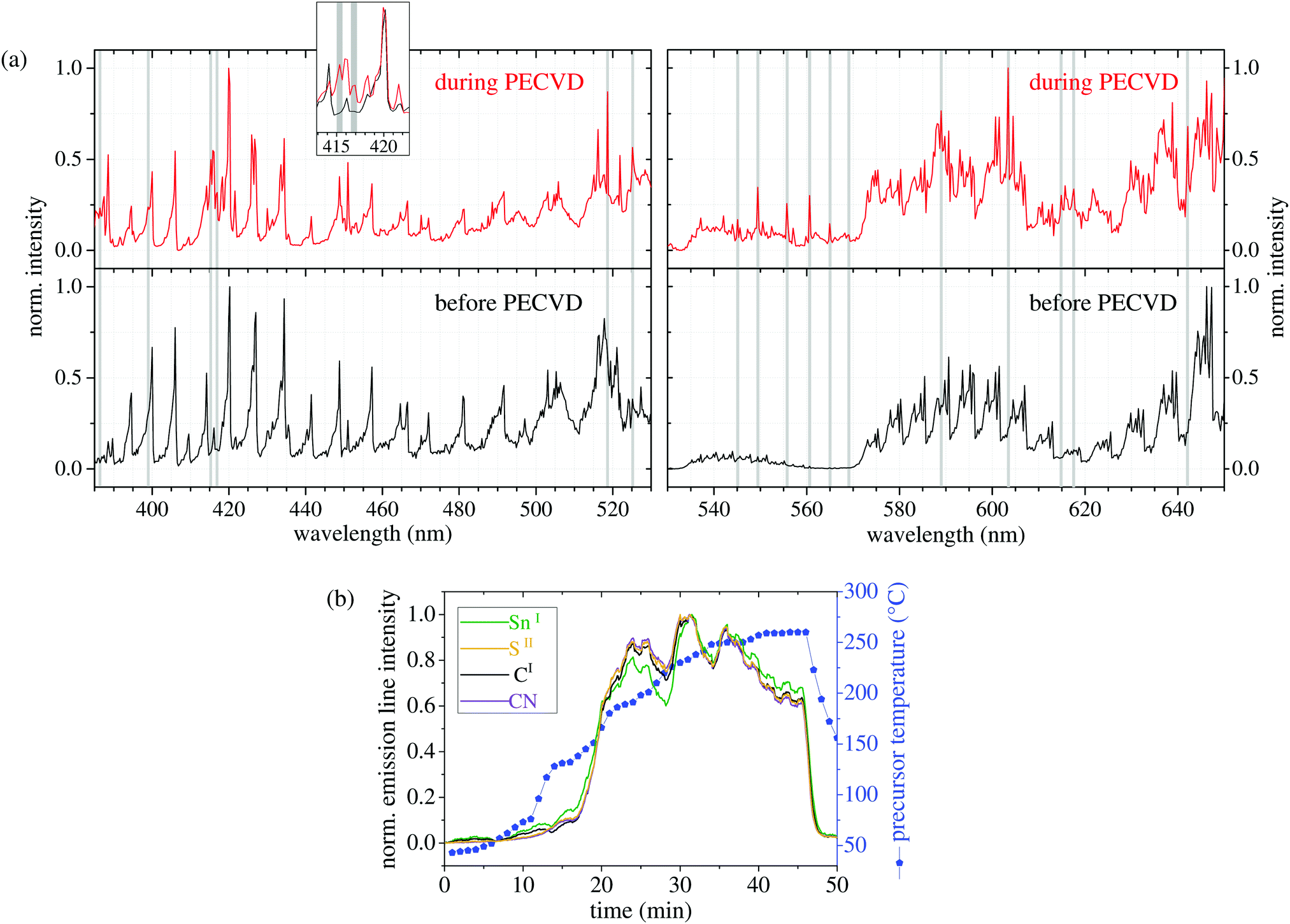 | ||
| Fig. 2 (a) Optical emission spectra of the plasma before (bottom) and during (top) the PECVD of SnS nanostructures at the same position of the plasma. The additional lines are highlighted with grey background. The assignment of atomic lines was done by using NIST atomic database.41 (b) Temporal development of the intensity of some selected additional emission lines during PECVD and precursor heating (CN at 416.8 nm, SII at 555.9 nm, CI at 603.1 nm, and SnI at 617.1 nm). | ||
According to our bond-energy calculations (Hybrid-DFT-functional B3LYP, Ahlrichs valence triple-zeta polarization basis set def2-TZVP, Gaussian 09W software) of the main precursor molecule, the observed fragmentation is likely to occur, when assuming a mean electron temperature Te of 2.8 eV, very roughly estimated via Boltzmann-plot technique. The bond between the tin center and the thiocarbamate ligands is the weakest bond with 2.3 eV, followed by the bond energy of the sulfur atoms to the carbon atoms within the ligand (2.8 eV). The energy for the abstraction of ethylene and methylene groups that leads to stable fragments of thiocyanate (NCS) and cyanide (CN) was calculated to be in the range of 3.0 to 3.3 eV. Actually, we find a weak OES signal at 385.8 nm during the SnS deposition that we relate to NCS according to ref. 42. Fig. 2(b) shows the development of the emission-line intensities over time at the same location in the plasma. Since the line intensities of all species follow the same trend with time, i.e., the intensities increase and decrease simultaneously, it can be assumed that the precursor evaporates undecomposed before it is activated by the plasma. If the precursor was decomposed into (volatile) organic and (involatile) inorganic species by thermal treatment before it reaches the plasma, the line intensity corresponding to Sn would exhibit a different temporal behavior from the other components, e.g., the carbon lines would arise first. Since the precursor heating changes over time (shown as blue line in Fig. 2(b)) the amount of released precursor also changes.
2.3 Plasma-enhanced chemical vapor deposition of tin sulfide
For the synthesis of vertically aligned, crystalline tin-sulfide nanowalls, we performed plasma-enhanced chemical vapor deposition (PECVD) using the above described tin-organic powder as a solid precursor. Highly toxic sulfur-containing gases like hydrogen sulfide are not required. Instead, sulfur and tin are provided by thermal evaporation of the precursor powder at low temperatures. Since, in the gas phase, tin and sulfur are still embedded in their molecular surrounding, due to the vaporization of the tin-organic compounds (see Section 2.2), the use of plasma gives access to the required reactive ionic tin and sulfur species by electron impact. For this, the precursor is heated up to 265 °C and the resulting vapor of mainly [Sn(dedtc)2] is released into a pulsed capacitively-coupled 13.56 MHz RF-plasma at 185 Pa chamber pressure and 20 W plasma power with argon and nitrogen as carrier gases. The specific conditions for the PECVD of SnS nanowalls have been optimized in an iterative process by systematically varying several reaction conditions. As a result, we found that mild plasma conditions and also plasma pulsing are crucial factors for the SnS-nanowall growth. Without plasma no deposition takes place, while the usage of a continuous plasma leads to the massive deposition of SnS. A pulsed plasma enables accurate nanostructured deposition of SnS. Beside an optimized plasma setup, the choice of substrate material affects the deposition. We used 1 × 1 cm2 metal-covered silicon wafers mounted face-down on a dielectric heating bar at a vertical distance of 2.8 cm from the precursor reservoir, also within the plasma area (see Experimental methods, Fig. 6). Elevated substrate temperatures are required for the deposition of high-quality films.43 A high substrate temperature enables a higher mobility of reactive species on the substrate surface, and thus facilitates processes of crystallization, recrystallization, and rearrangement, leading to a higher film quality. However, higher substrate temperatures can also increase the deposition rate, which needs to be regulated when nanostructuring is purposed. Using a high substrate temperature of 400 °C, our PECVD procedure leads to square-shaped nanosheet stacks covering the entire substrate surface. An SEM image is shown in Fig. 3(a). | ||
| Fig. 3 (a) SEM image of PECVD-grown SnS structures with (b) corresponding XRD pattern and reference data for α-SnS (ICDD pattern no. 39-0354). Reflexes marked with “Δ” are those from the wafer, “*” indicates (111) gold reflex. For better visibility of reflexes with lower intensity, part of the ordinate is cut off. (c) Representative EDX spectrum of the sample. | ||
Looking at the microscale stacking, a layered structure is clearly visible, indicating anisotropic crystal growth. The frayed shape of the edge structure reveals the growth direction to be towards the edges. The corresponding powder X-ray diffraction pattern (Fig. 3(b)) matches accurately to the reference pattern of orthorhombic α-SnS,44 proving the high quality of the structure. Four additional reflexes at 33.05°, 38.26°, 47.81°, and 56.42° originate from the gold-covered wafer substrate. There is no evidence for any crystalline subphase, i.e., neither typical reflexes for SnS2 (15.14°, 32.38°, 42.22°)45 nor for Sn2S3 (16.10°, 31.88°, 46.90°)46 has been detected. The deviation in relative reflex intensities can be attributed to texture effects. EDX analysis (Fig. 3(c)) proves the 1![[thin space (1/6-em)]](https://www.rsc.org/images/entities/char_2009.gif) :1 ratio of tin to sulfur in the reaction product and the absence of organic species. Since the precursor was heated up to only 265 °C, no SnO2 has been released into the plasma and thus no oxygen contamination of the tin-sulfide structures occurred. We assume that at 265 °C precursor heating only the compounds [S2Sn2(dedtc)4] and [Sn(dedtc)2] are released into the plasma leading to a tin-to-sulfur ratio of 1:5–1:4 in the plasma. Even though the amount of sulfur in the plasma is considerably higher than the amount of tin, only SnS is formed. This can be explained by the fact that α-SnS is the thermodynamically most stable phase among the various SnxSy phases. According to Skelton et al.3 orthorhombic α-SnS (Pnma) represents the ground-state. Phases like tin sesquisulfide (Sn2S3) are predicted to be less stable and to decompose into α-SnS and SnS2 at certain conditions.3 It has to be noted, that besides the Pnma phase, the newly discovered π-cubic phase (Cmcm) is also dynamically stable3 (2.2 kJ mol−1 above the ground state47).
:1 ratio of tin to sulfur in the reaction product and the absence of organic species. Since the precursor was heated up to only 265 °C, no SnO2 has been released into the plasma and thus no oxygen contamination of the tin-sulfide structures occurred. We assume that at 265 °C precursor heating only the compounds [S2Sn2(dedtc)4] and [Sn(dedtc)2] are released into the plasma leading to a tin-to-sulfur ratio of 1:5–1:4 in the plasma. Even though the amount of sulfur in the plasma is considerably higher than the amount of tin, only SnS is formed. This can be explained by the fact that α-SnS is the thermodynamically most stable phase among the various SnxSy phases. According to Skelton et al.3 orthorhombic α-SnS (Pnma) represents the ground-state. Phases like tin sesquisulfide (Sn2S3) are predicted to be less stable and to decompose into α-SnS and SnS2 at certain conditions.3 It has to be noted, that besides the Pnma phase, the newly discovered π-cubic phase (Cmcm) is also dynamically stable3 (2.2 kJ mol−1 above the ground state47).
2.4 PECVD of tin-sulfide nanowalls
In order to maximize the surface area of the SnS nanostructures we optimized the reaction conditions to avoid the massive stacking of the sheets. The final goal was to establish a geometry as it is typical for carbon nanowalls.26 For carbon-nanowall formation, it has been shown that grain boundaries play a crucial role, according to Zhu et al.48 During the first few minutes of the synthesis, the formation of a 1–15 nm thick layer of graphitic sheets is described, which grows parallel to the substrate. Once a sufficient level of force develops at the grain boundaries, vertical, diffusion-controlled growth is enabled.48 It has been shown that the growth of the carbon nanowalls mainly takes place at the top of the sheets.49 The vertical growth of free-standing nanosheets is further enhanced by a vertical electric field.48 Transferring the necessity of a grain-boundary rich base layer for nanowall formation to the case of SnS, our PECVD was changed in a way that small sheets are deposited instead of massive stacks. For this, we drastically decreased the deposition rate by lowering the substrate temperature from 400 °C to 250 °C. All other parameters were kept the same. Actually, we observed that the substrate temperature not only influences the deposition rate, but also the morphology of the deposited structures: the lower the substrate temperature, the smaller and the slenderer the structures become. At a substrate temperature of 250 °C, flaky structures predominantly grow parallel to the substrate. Due to the resulting patch-like texture, the coating features numerous thin grain boundaries (see Fig. S2(a), ESI†). The corresponding XRD pattern can be assigned to phase-pure orthorhombic α-SnS. Due to strong texture effects and the small layer thickness, most of the reflexes of the XRD pattern of the sample synthesized at 250 °C substrate temperature are hard to identify (see Fig. S2(b), ESI†). However, the (040) reflex is unambiguously dominant, indicating that the interlayer periodicity and thus the basal plane of the nanosheets, is parallel to the substrate and that (040) represents the sheet thickness. Although an essential condition for nanowall formation seems to be given by the grain-boundary rich layer formed from SnS flakes, the formation of nanowall-like SnS structures does not take place. A possible reason might be the thin gold coverage of the wafer substrate, which originally was intended to gain surface roughness and to increase the adhesion of tin and sulfur species to the substrate. We suspect a relation between crystalline gold surfaces and SnS growth: the XRD patterns of the samples with gold coverage show a broad reflex at 38.3° (see Fig. 3(b)) that can be assigned to the (111) reflex of gold.50 Due to the weak adhesion of gold to the smooth wafer surface, gold shows a considerable mobility on the substrate. If the gold layer is very thin, the dewetting leads to the formation of individual gold islands with (111) crystal facets. Plasma-activated species diffuse on the wafer surface and can attach to these islands. From our observation, vertical SnS growth is suppressed by the [111] surface of gold. Actually, we also observed solely planar growth of SnS when using a bare [111] silicon substrate without gold coverage. However, the deposition was much less than with gold layer. Hence, for the vertical growth of SnS nanowalls, we tried to increase the adhesion ability of the substrate by a wafer coverage, but at the same time avoid the formation of (111) facets. For this, we sputtered 20 nm of an amorphous layer, namely steel/18Cr/9Ni, on a [100] silicon wafer and performed the pulsed PECVD procedure at 250 °C substrate temperature and 265 °C precursor heating for 30 min. As a result, the entire substrate surface was homogeneously covered with a dull, deep black opaque layer. The corresponding SEM image in Fig. 4(a) shows a dense layer of vertically aligned ultrathin nanowalls (average thickness of approx. 14 nm). Via cross-sectional imaging, a height of ca. 3.5 μm was measured. The corresponding XRD pattern (Fig. 4(b)) fits accurately to orthorhombic α-SnS with no notable sub-phases. Moreover, there are no reflexes besides SnS and wafer substrate, proving the amorphous condition of the previously sputtered alloy. Electron diffraction of detached single nanowalls indicate the lateral extent from bottom to top to be along (001), that is described to exhibit enhanced electron mobility. | ||
| Fig. 4 (a) Top-view and cross-sectional SEM image of thin SnS nanowalls grown on silicon wafer sputter-coated with 20 nm steel/18Cr/9Ni alloy. The substrate temperature during PECVD was set at 250 °C, the precursor was heated up to 265 °C. (b) XRD pattern of the thin nanowalls (Δ = wafer) and reference data of orthorhombic α-SnS (ICDD pattern no. 39-0354). (c) Top-view and cross-sectional SEM image of SnS/SnS2 nanowalls grown on silicon wafer sputter-coated with 20 nm steel/18Cr/9Ni. (d) XRD pattern of the SnS/SnS2 nanowalls and reference data of hexagonal SnS2 (ICDD pattern no. 23-0677). | ||
Obviously, in contrast to gold, the thin steel/18Cr/9Ni layer enables the formation of SnS nanowalls. This might be due to different synergetic effects. First, the different solid-state dewetting (SSD) of gold and the used alloy on silicon wafers influences the deposition. The SSD depends on the interface energy between the metal film and the substrate as well as the reduction of the surface energy by, e.g., thermal annealing.51 Gold is known to form single-crystalline islands with flat (111) textured top surfaces.52,53 Plasma-induced SSD even enables the formation of (uniform) gold nanoparticles by hole nucleation and growth at the grain boundaries.54 We also observed SSD of the steel/18Cr/9Ni layer on the wafer surface. After plasma and heat treatment, the smooth as-deposited layer turned into nanoparticle-like structures with an average height of 14 nm and an average width of 35 nm. Via atomic-force microscopy (AFM) we measured an increase of the alloy-layer roughness (RRMS) from 0.16 to 2.06 (compare ITO: RRMS = 2.77). However, using other “rough substrates” such as ITO-covered glass slides as substrates for our PECVD procedure does not lead to nanowall formation. Hence, beside roughness, a catalytic activity of the steel/18Cr/9Ni alloy might be present. Since the dewetting behavior of the alloy implies a (at least partial) melting on the wafer surface, a solution of tin and/or sulfur in the liquid alloy might be possible. Herman and coworkers55 determined the solubility of tin in α-Fe to be 6.5 w% at 600 °C and that the addition of 1 w% nickel or 1 w% chromium lowers the solubility of tin to 5.2 w%. According to Herrnstein et al.56 sulfur has a very low solubility in iron, i.e., 0.001 atomic% at 600 °C. Due to the low solubility of tin and sulfur in the alloy, the saturation limit is low, and thus crystallization of SnS might occur at an early stage of the synthesis. This hypothesis is reinforced by the fact that nickel and iron can form a type-2 binary sulfide system, which is characterized by the appearance of an eutectic point.57 Thus, a kind of vapor–liquid–solid (VLS) process might promote the SnS formation. This might be enhanced by the plasma conditions, since plasma lowers the surface tension in Fe–Ni–Cr(–S) alloys.58 Applying this model to the SnS deposition using gold-covered wafers as substrates, a VLS-like process is not likely. Tin and sulfur do not dissolve in gold. Instead, sulfur–gold interfaces are formed at the (111) gold facets via chemical or coordinating bonding.59 Consequently, the shape of the resulting SnS layer strongly depends on the processes in the earliest stages of the PECVD directly on the substrate surface.
2.5 SnS/SnS2-heterostructure formation
For the pulsed PECVD of α-SnS we limited the precursor heating to 265 °C. Performing our pulsed PECVD at an elevated precursor heating of up to 510 °C, nanowall structures with an average thickness of 48 nm grow on steel/18Cr/9Ni-covered silicon wafers as shown in the SEM images in Fig. 4(c). Regarding the corresponding X-ray diffraction pattern, shown in Fig. 4(d), some reflexes can be assigned to hexagonal SnS2, e.g., at 15.05°, indicating the thick nanowalls to be a mixed structure of SnS and SnS2. Cross-sectional Raman mapping of the sample does not show a distinct phase-junction from SnS to SnS2, implying that these two species do not form separate macroscopic domains, but are mixed at the nanometer scale. Hence, it is likely that SnS was partially post-sulfurized in consequence of an increased partial pressure of sulfur in the plasma. Considering that the SnS2 formation only occurs at high precursor heating, two possible scenarios for an increase in sulfur content in the gas phase can be drafted. At low pressure and low precursor heating of up to 265 °C, only the compounds [S2Sn2(dedtc)4] and [Sn(dedtc)2] are evaporated, leading to a molar ratio of tin-to-sulfur of 1:5–1:4 in the plasma. Phase-pure SnS is formed. Extending the precursor heating to temperatures over 400 °C at low pressure, the compound with the highest sulfur content, namely [Sn(dedtc)4], starts to evaporate, leading to an increased partial pressure of sulfur in the plasma. It is also very likely that the vaporization of the precursor at low pressure is increasingly accompanied by decomposition with increasing precursor heating. Considering ref. 34 and 39, sulfur-containing organic fragments are released, while an inorganic residue remains. Consequently, the sulfur content in the plasma is increased, causing a subsequent sulfurization of the previously grown SnS.
2.6 Conductivity measurements
In order to get an idea of the electronic properties of the PECVD-grown SnS and SnS/SnS2 nanostructures, and to examine, whether the nanosheet network is appropriate for application in electronic devices, I–V curves of the stacked SnS, SnS nanowalls, and SnS/SnS2 heteronanowalls were measured. Due to the extraordinary roughness of the deposited layers, we used mercury droplets, fixed via stainless-steel cannulas (distance 5 mm), for electrical contact with the structures. At ambient conditions, the voltage was swept at a scan rate of 50 mV s−1 and the resulting current was measured. Representative I–V curves of each sample are shown in Fig. 5. All measured samples were synthesized as described above, but on Si/SiO2 [100] wafers with 500 nm SiO2 instead of 100 nm, to exclude any leakage current through the substrate. Moreover, we verified that the metal coverage of the substrate did not enable charge transport by measuring plasma-treated annealed metal-covered wafers. Due to the metal-layer dewetting, no significant current is transported, so that the only conductive part of the samples is the respective PECVD-grown nanostructure network. | ||
| Fig. 5 Representative I–V curves of mercury–droplet contacted stacked SnS (black), thick SnS/SnS2 nanowalls (yellow) and thin SnS nanowalls (blue). Inset image shows work function of mercury and band gaps of SnS and SnS2 according to Burton et al.60 | ||
The representative measurement of the stacked SnS structures is shown in black. Due to the Schottky-type contact between mercury droplet and SnS structure, the curve shows a slight bending around the coordinate origin. Taking the geometry of the conducting channel into account, a specific conductivity of 26 S m−1 was calculated by evaluating the linear slope of the curve in the region of ±0.2 V. In comparison, the thin SnS nanowalls were measured identically. The corresponding blue curve in Fig. 5 shows a much higher absolute current, already indicating a higher conductivity than the stacked structures. Also the curve bending is stronger, suggesting an increased Schottky barrier that might be caused by an increased band gap of SnS due to quantization effects resulting from the small thickness of the individual nanosheets. Since the contact area between mercury droplet and nanowalls is not precisely known, we estimated an active contact surface of 20%, resulting in a calculated specific conductivity of approx. 260 S m−1. The calculated specific conductivity of the investigated tin-sulfide samples as a function of channel width, i.e., as a function of the active contact area of mercury droplet and structure is shown in the ESI† (Fig. S3). Finally, we also measured I–V curves of the thick heterostructured nanowalls, shown as yellow curve in Fig. 5. The absolute current is in a range between the stacked SnS and the SnS nanowalls, which was expected, since SnS2 has a lower electrical conductivity compared to SnS.61 The bending indicates a Schottky-type contact. If the thick nanowalls were phase-pure SnS2, this bending would not appear, since the band alignment, shown in the inset in Fig. 5, would not lead to the formation of a Schottky barrier. Hence, the bending supports the hypothesis, that the thick nanowalls are SnS/SnS2 heterostructures since, in this case, a Fermi-level shift towards higher energies results in a Schottky barrier.
The very simple I–V curve measurements demonstrate, that charge transport through a dense network of very thin nanowalls is much more efficient in comparison to charge transport through stacked SnS. Since the footprint of the mercury droplet is relatively small, only a few nanowalls are contacted. Consequently, the horizontal contribution to the absolute current is much higher than the (actual preferred) vertical contribution. The more nanowalls are contacted, as it would be the case in a solar cell, the more the vertical charge transport comes into effect. Hence, an even higher conductivity is expected. Covering the nanowalls with an appropriate conductive polymer would enable the generation of a boundary layer for charge separation and would exclude short-circuits that could occur when the bare SnS layer is conventionally contacted.
3 Conclusion
We report on a novel PECVD approach for the large-area deposition of crystalline, well-aligned SnS nanowalls. The used solid single-source precursor is synthesized by a simple precipitation reaction of SnCl2·2H2O and Na(dedtc)·3H2O in water. Combining 119Sn-MAS NMR spectroscopy with single-crystal data and thermogravimetric analysis, reveals that the precursor powder mainly consists of [Sn(dedtc)2] with side-products of [S2Sn2(dedtc)4] and [Sn(dedtc)4]. The vertical CCP setup allows the direct evaporation of the solid tin-organic precursor. Via optical emission spectroscopy, we investigate the precursor fragmentation upon plasma impact. Here, the release of activated tin and sulfur species is indicated by additional emission lines in the spectrum occurring during the SnS deposition.Tuning the morphology of the PECVD-grown structures from stacks to vertically aligned sheets allows the following conclusions: (1) at an elevated substrate temperature of 400 °C, the deposition rate is high and SnS stacks are formed. (2) At a low substrate temperature of 250 °C, the temperature is not the morphology-determining parameter. Now, the interaction between the plasma-activated species and the substrate surface becomes more relevant. It turns out, that (111) facets suppress the vertical growth of SnS. (3) A certain surface roughness is needed to increase the retention time of the reactants on the substrate surface and thus to deposit considerable amounts of SnS. Grain boundaries play a crucial role for vertical growth. It turns out, that a thin layer of steel/18Cr/9Ni on the silicon wafer is an appropriate ground for SnS-nanowall growth. The non-crystalline material features an enhanced surface roughness upon dewetting. However, since ITO-covered glass slides are not suitable for SnS-nanowall formation, an additional aspect has to be taken into account. (4) We assume that the morphology of the deposited structures strongly depends on the very early processes of the deposition. This includes the physical and chemical interaction between the reactive species and the substrate surface. For gold, a chemical bonding to sulfur can be assumed. In the case of steel/18Cr/9Ni, the dissolution of small amounts of tin is expected. The resulting binary system is able to dissolve sulfur, resulting in an eutectic mixture. Small amounts of chromium and nickel further decrease the supersaturation limit of the dissolved tin sulfide. Consequently, a VLS-like SnS-nanowall growth is assumed.
SnS/SnS2 heteronanowalls are achieved by extending the precursor heating from 265 °C to 510 °C. A partial post-sulfurization of SnS forming SnS/SnS2 is assumed as a consequence of an increased partial pressure of sulfur in the plasma at elevated precursor heating. Finally, simple I–V curve measurements prove the significantly enhanced conductivity through the vertically aligned SnS-sheet network compared to stacked SnS. Hence, the full functionality of SnS as absorber layer in optoelectronic devices might become accessible by aligned nanostructured SnS.
Further experiments will focus on the optimization of the PECVD of SnS nanowalls on FTO-covered glass substrates in order to study the absorption properties, the electric performance and the photo conductivity in more detail. Moreover, covering the tin-sulfide nanowall layer with a conductive polymer that can be contacted conventionally will be the next step to realize a SnS-nanowall based solar cell.
4 Experimental methods
4.1 Chemicals
Argon (Ar, Westfalen, 5.0), gold (999.9 fineness, PIM), steel/18Cr/9Ni, nitrogen (N2, Westfalen, 5.0), sodium diethyldithiocarbamate trihydrate (C5H10NNaS2·3H2O, Sigma Aldrich), tin dichloride dihydrate (SnCl2·2H2O Sigma Aldrich). All chemicals were used without further purification.4.2 Precursor synthesis
For the synthesis of bis(diethyldithiocarbamato)tin(II), 1.59 g (7.0 mmol) tin dichloride dihydrate and 3.21 g (15 mmol) sodium diethyldithiocarbamate trihydrate were dissolved in 50 mL fresh ultrapure water, respectively. At 900 rpm stirring and light-exclusion, the sodium diethyldithiocarbamate solution was added dropwise to the tin dichloride solution. When approx. 30 mL thiocarbamate solution was added, a bright yellow precipitate became visible. After the addition of 50 mL thiocarbamate solution, the suspension was stirred at 900 rpm under light-exclusion for 15 min. Then the precipitate was allowed to sediment in order to decant the cloudy supernatant. The yellow solid was washed with ultrapure water until the whitish residue was removed. The product was then dried under vacuum (1 mbar abs.) for 48 h and was stored at dry inert conditions. For the fabrication of a reference sample, the as-described dropwise precipitation of tin dichloride dihydrate with sodium diethyldithiocarbamate trihydrate was performed identically, but in dried degassed methanol under nitrogen atmosphere.4.3 Substrate preparation
Prime grade silicon wafers with a 100 nm thermally oxidized layer were purchased from Addison Engineering, Inc. San Jose, CA. The surface crystal orientation of the 625 μm thick n-type doped wafers was [100]. Before usage, the 1 × 1 cm2 wafer pieces were sonicated in acetone for 15 min and dried under nitrogen flow. For PECVD the wafer piece was then coated with 20 nm gold without undercoating using thermal high-vacuum coater Classic 250 (Pfeiffer Vacuum). The gold-coated wafer was subsequently inserted into the PECVD setup. For each synthesis, a freshly coated wafer was used. Similarly, wafers were also covered with 20 nm of steel/18Cr/9Ni by sputtering using a Gatan 682 Precision Etching and Coating System (PECS).4.4 Plasma-enhanced chemical vapor deposition
The plasma-enhanced chemical vapor deposition was performed using a home-built setup where a capacitively-coupled plasma with a radio frequency of 13.56 MHz and an argon–nitrogen mixture as carrier gas was used. In general, 185 mg of the precursor were placed on a resistance-heating plate in vertical alignment with a heatable substrate holder that holds a metal-coated Si/SiO2 [100] wafer face-down. A scheme of the setup is shown in Fig. 6. The closed reactor was conditioned with a mixture of 92% argon and 8% nitrogen. For the synthesis, the chamber pressure is set to 1.9 mbar at an argon flow of 139 sccm and a nitrogen flow of 12 sccm. After two minutes of continuous plasma, the plasma is set into pulsed mode (1 s at 50% duty cycle). Then the substrate is heated at a rate of approx. 30 °C min−1 until the substrate temperature is reached. Subsequently, the precursor is heated (approx. 8 °C min−1). The formal reaction time was started when a color change of the wafer indicated the deposition of material. After a certain reaction time, the precursor heating was stopped. By the time the plasma color indicates no further existence of precursor in the plasma, the plasma is turned off. After five more minutes the substrate was allowed to cool down to room temperature before removing.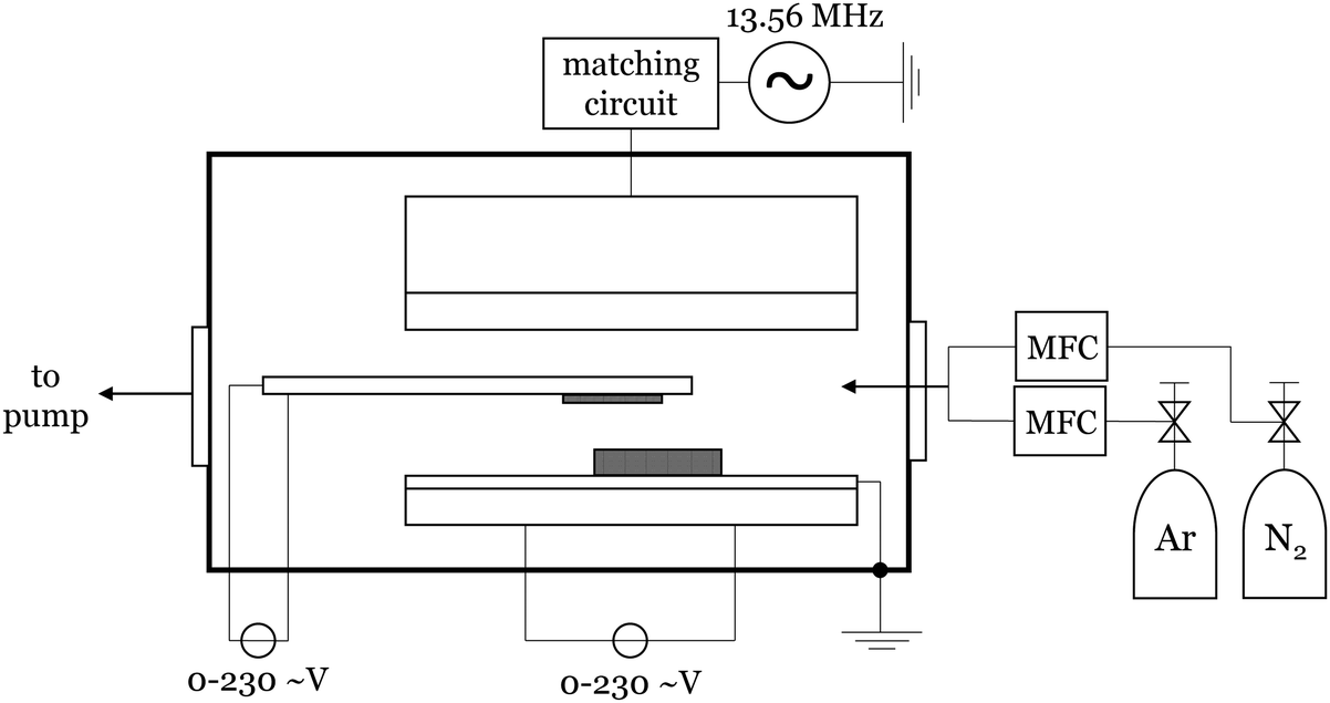 | ||
| Fig. 6 Technical scheme of the used home-built PECVD setup (CCP, 13.56 MHz RF). In between the electrodes a dielectric Si3N4 heating bar is holding the wafer substrate face down. The precursor is placed in a molybdenum boat on the grounded heatable electrode. | ||
4.5 Solid-state NMR spectroscopy
Solid-state NMR experiments were performed on a Bruker Avance II 400 spectrometer, equipped with 4 or 2.5 mm double resonance MAS probe. 119Sn{1H} cross-polarization (CP) magic angle spinning (MAS) NMR spectra were acquired using ramped polarization transfer at an operating frequency of 149.20 MHz and two-pulse phase-modulated (TPPM) decoupling during acquisition. 119Sn Hahn echo MAS NMR spectra were acquired to reduce rolling in background with rotor-synchronization during tau intervals. Chemical shifts were referenced to external standard of tetramethyltin, at 0 ppm. Repetition delays were typically 10 s and the spinning frequencies were either 14 or 30 kHz.4.6 Thermogravimetric analysis
Thermogravimetric analysis (TGA) of the precursor powder and pure Sn(dedtc)2 was performed using the STA 449 F3 Jupiter (Netzsch) with a heating rate of 5 °C min−1 at normal pressure and argon flow.4.7 Optical emission spectroscopy
For recording the optical-emission spectra we imaged the inside of the plasma chamber onto the entrance slit of a 300 mm spectrograph (SpectraPro 2300i, Princeton Instruments). This is done by collecting the light with a 300 mm lens through a quartz window in the chamber and focusing into the spectrograph with a 100 mm lens. Inside the spectrograph the light is dispersed by a 300 lines per mm grating onto the two dimensional array of a cooled low noise charge-coupled device (CCD) camera (iDUS, Andor). Using the entrance slit in horizontal direction and a distinct choice of CCD pixels in vertical direction only light from the region of interest inside the chamber is chosen to build up the optical emission spectra. Spatial resolution was achieved by using a mirror scanner. For the in situ spectroscopy, a typical PECVD procedure was performed, while spectra were measured (3 s exposure time) at the same position of the plasma bulk. The first spectrum was subtracted as baseline from every following spectrum of the experiment. Data processing was performed using the software Andor Solis, evaluation was done using MATLAB R2017a.4.8 Scanning electron microscopy
Scanning electron microscopy (SEM) was performed to visualize the topography of the CVD-grown structures in top-view and cross-sectional view using a Quanta 3D FEG (FEI) with a beam energy of 20 kV at high vacuum. All samples were measured in the original state without any pre-treatment.4.9 Energy-dispersive X-ray spectroscopy
An EVO MA 10 (Zeiss) scanning electron microscope was used in order to investigate the elemental composition of the precursor and the CVD-grown samples. The beam energy was 20 kV and the beam current was 1.2 nA. The spectra were analyzed via INCA software.4.10 Powder X-ray diffraction
All samples were investigated via powder X-ray diffraction using an X'pert Pro MPD (Philips) in the range of 5 to 60° using Cu K-α source (λ = 1.54 Å). For each measurement, the entire sample was placed on a substrate holder. The data were processed using X'pert Pro software. Sonneveld & Visser method was performed for background correction.Conflicts of interest
The authors declare no competing interests.Acknowledgements
The authors thank Almut Barck for XRD measurements, Birger Dittrich for diffraction experiments, Marcel Dohrmann for bond-energy calculations, Maximilian Schwarz and Angelique Rieckmann for helpful discussions, and Jan Flügge, Michael Höltig and Dennis Bonatz for technical support. C. R. gratefully acknowledges financial support from Pro Exzellenzia 4.0 (project of the European Social Fund and the BWFG Hamburg).References
- W. Albers, C. Haas and F. van der Maesen, J. Phys. Chem. Solids, 1960, 15, 306–310 CrossRef CAS.
- K. F. Mak and J. Shan, Nat. Photonics, 2016, 10, 216–226 CrossRef CAS.
- J. M. Skelton, L. A. Burton, F. Oba and A. Walsh, J. Phys. Chem. C, 2017, 121, 6446–6454 CrossRef CAS PubMed.
- Z. Tian, C. Guo, M. Zhao, R. Li and J. Xue, ACS Nano, 2017, 11, 2219–2226 CrossRef CAS PubMed.
- C. Xin, J. Zheng, Y. Su, S. Li, B. Zhang, Y. Feng and F. Pan, J. Phys. Chem. C, 2016, 120, 22663–22669 CrossRef CAS.
- K. Hartman, J. Johnson, M. I. Bertoni, D. Recht, M. J. Aziz, M. A. Scarpulla and T. Buonassisi, Thin Solid Films, 2011, 519, 7421–7424 CrossRef CAS.
- R. Banai, M. Horn and J. Brownson, Sol. Energy Mater. Sol. Cells, 2016, 150, 112–129 CrossRef CAS.
- N. P. Dasgupta, X. Meng, J. W. Elam and A. B. F. Martinson, Acc. Chem. Res., 2015, 48, 341–348 CrossRef CAS PubMed.
- N. Koteeswara Reddy, Y. B. Hahn, M. Devika, H. R. Sumana and K. R. Gunasekhar, J. Appl. Phys., 2007, 101, 093522 CrossRef.
- J. Vidal, S. Lany, M. d'Avezac, A. Zunger, A. Zakutayev, J. Francis and J. Tate, Appl. Phys. Lett., 2012, 100, 032104 CrossRef.
- Y. Gupta and P. Arun, Phys. Status Solidi B, 2016, 253, 509–514 CrossRef CAS.
- P. Sinsermsuksakul, L. Sun, S. W. Lee, H. H. Park, S. B. Kim, C. Yang and R. G. Gordon, Adv. Energy Mater., 2014, 4, 1400496 CrossRef.
- Y.-B. Yang, J. K. Dash, Y. Xiang, Y. Wang, J. Shi, P. H. Dinolfo, T.-M. Lu and G.-C. Wang, J. Phys. Chem. C, 2016, 120, 13199–13214 CrossRef CAS.
- R. W. Miles, O. E. Ogah, G. Zoppi and I. Forbes, Thin Solid Films, 2009, 517, 4702–4705 CrossRef CAS.
- R. Chakraborty, V. Steinmann, R. Jaramillo, K. Hartman, R. E. Brandt, H. H. Park, J. Poindexter, Y. S. Lee, R. G. Gordon and T. Buonassisi, Photovoltaic Specialist Conference (PVSC), 2014 IEEE 40th, 2014, pp. 2304–2306 Search PubMed.
- H. Kafashan, F. Jamali-Sheini, R. Ebrahimi-Kahrizsangi and R. Yousefi, Int. J. Miner., Metall. Mater., 2016, 23, 348–357 CrossRef CAS.
- F. Niknia, F. Jamali-Sheini and R. Yousefi, J. Electron. Mater., 2015, 44, 4734–4739 CrossRef CAS.
- R. E. Banai, H. Lee, M. A. Motyka, R. Chandrasekharan, N. J. Podraza, J. R. S. Brownson and M. W. Hom, IEEE J. Photovolt., 2013, 3, 1084–1089 Search PubMed.
- Z. Mutlu, S. Shahrezaei, S. Temiz, M. Ozkan and C. S. Ozkan, J. Electron. Mater., 2016, 45, 2115–2120 CrossRef CAS.
- I. P. Parkin, L. S. Price, T. G. Hibbert and K. C. Molloy, J. Mater. Chem., 2001, 11, 1486–1490 RSC.
- K. Ramasamy, V. L. Kuznetsov, K. Gopal, M. A. Malik, J. Raftery, P. P. Edwards and P. O'Brien, Chem. Mater., 2013, 25, 266–276 CrossRef CAS.
- P. Kevin, D. J. Lewis, J. Raftery, M. Azad Malik and P. O'Brien, J. Cryst. Growth, 2015, 415, 93–99 CrossRef CAS.
- I. Y. Ahmet, M. S. Hill, A. L. Johnson and L. M. Peter, Chem. Mater., 2015, 27, 7680–7688 CrossRef CAS.
- Y. Wang, Y. B. K. Reddy and H. Gong, J. Electrochem. Soc., 2009, 156, H157–H160 CrossRef CAS.
- J.-P. Park, M.-Y. Song, W.-M. Jung, W.-Y. Lee, J.-H. Lee, H.-G. Kim and I.-W. Shim, Bull. Korean Chem. Soc., 2012, 33, 3383–3386 CrossRef CAS.
- M. Höltig, C. Ruhmlieb, C. Strelow, T. Kipp and A. Mews, Z. Phys. Chem., 2015, 229, 301–316 Search PubMed.
- M. Höltig, C. Ruhmlieb, T. Kipp and A. Mews, J. Phys. Chem. C, 2016, 120, 7476–7481 CrossRef.
- A. Ortiz, J. C. Alonso, M. Garcia and J. Toriz, Semicond. Sci. Technol., 1996, 11, 243–247 CrossRef CAS.
- A. Sanchez-Juarez and A. Ortiz, Semicond. Sci. Technol., 2002, 17, 931–937 CrossRef CAS.
- L. L. Cheng, M. H. Liu, S. C. Wang, M. X. Wang, G. D. Wang, Q. Y. Zhou and Z. Q. Chen, Semicond. Sci. Technol., 2013, 28, 015020 CrossRef.
- S. Wang, S. Wang, J. Chen, P. Liu, M. Chen, H. Xiong, F. Guo and M. Liu, J. Nanopart. Res., 2014, 16, 2610 CrossRef.
- L. Cheng, M. Liu, M. Wang, S. Wang, G. Wang, Q. Zhou and Z. Chen, J. Alloys Compd., 2012, 545, 122–129 CrossRef CAS.
- D. Perry and R. A. Geanangle, Inorg. Chim. Acta, 1975, 13, 185–189 CrossRef CAS.
- G. Bratspies, J. Smith, J. Hill and R. Magee, Thermochim. Acta, 1978, 27, 307–317 CrossRef CAS.
- R. Selvaraju and K. Panchanatheswaran, Polyhedron, 1994, 6/7, 903–908 CrossRef.
- B. F. Hoskins, R. L. Martin and N. M. Rohde, Aust. J. Chem., 1976, 29, 213–217 CrossRef CAS.
- C. Preti, G. Tosi and P. Zannini, J. Mol. Struct., 1980, 65, 283–292 CrossRef CAS.
- C. Cossement, J. Darville, J.-M. Gilles, J. B. Nagy, C. Fernandez and J.-P. Amoureux, Magn. Reson. Chem., 1992, 30, 263–270 CrossRef CAS.
- G. Barone, T. Chaplin, T. G. Hibbert, A. T. Kana, M. F. Mahon, K. C. Molloy, I. D. Worsley, I. P. Parkin and L. S. Price, J. Chem. Soc., Dalton Trans., 2002, 6, 1085–1092 RSC.
- C. A. Stewart, D. A. Dickie, Y. Tang and R. A. Kemp, Inorg. Chim. Acta, 2011, 376, 73–79 CrossRef CAS.
- A. Kramida, Y. Ralchenko, J. Reader and N. A. Team, NIST Atomic Spectra Database, 2018.
- R. Pearse and A. Gaydon, The Identification of Molecular Spectra, Chapman and Hall, London/Wiley, New York, 4th edn, 1976 Search PubMed.
- J. R. Bottin, P. R. McCurdy and E. R. Fisher, Rev. Sci. Instrum., 1997, 68, 2149–2155 CrossRef CAS.
- H. Wiedemeier and G. von Schnering, Z. Kristallogr., 1978, 148, 295–303 CrossRef CAS.
- I. Oftedal, Norsk Geol. Tidsskr, 1927, 9, 225–233 CAS.
- M. Cruz, J. Morales, J. Espinos and J. Sanz, J. Solid State Chem., 2003, 175, 359–365 CrossRef CAS.
- J. M. Skelton, L. A. Burton, F. Oba and A. Walsh, APL Mater., 2017, 5, 036101 CrossRef.
- M. Zhu, J. Wang, B. C. Holloway, R. Outlaw, X. Zhao, K. Hou, V. Shutthanandan and D. M. Manos, Carbon, 2007, 45, 2229–2234 CrossRef CAS.
- K. Davami, M. Shaygan, N. Kheirabi, J. Zhao, D. A. Kovalenko, M. H. Rümmeli, J. Opitz, G. Cuniberti, J.-S. Lee and M. Meyyappan, Carbon, 2014, 72, 372–380 CrossRef CAS.
- S. Pedireddy, H. K. Lee, W. W. Tjiu, I. Y. Phang, H. R. Tan, S. Q. Chua, C. Troadec and X. Y. Ling, Nat. Commun., 2014, 5, 4947 CrossRef CAS PubMed.
- G. Seguini, J. Llamoja Curi, S. Spiga, G. Tallarida, C. Wiemer and M. Perego, Nanotechnology, 2014, 25, 495603 CrossRef CAS PubMed.
- A. B. Tesler, B. M. Maoz, Y. Feldman, A. Vaskevich and I. Rubinstein, J. Phys. Chem. C, 2013, 117, 11337–11346 CrossRef CAS.
- M. Kang, S.-G. Park and K.-H. Jeong, Sci. Rep., 2015, 5, 14790 CrossRef CAS PubMed.
- S.-H. Kwon, H. J. Choe, H.-C. Lee, C.-W. Chung and J.-J. Lee, J. Nanosci. Nanotechnol., 2013, 13, 6109–6114 CrossRef CAS PubMed.
- M. Nageswararao, C. J. McMahon and H. Herman, Metall. Trans., 1974, 5, 1061–1068 CrossRef CAS.
- W. Herrnstein, F. Beck and M. Fontana, Trans. AIME, 1968, 242, 1049–1056 CAS.
- G. Kullerud, Mineral. Soc. Am., Spec. Pap., 1970, 3, 199–210 Search PubMed.
- M. J. McNallan and T. Debroy, Metall. Trans. B, 1991, 22, 557–560 CrossRef.
- E. Pensa, E. Cortés, G. Corthey, P. Carro, C. Vericat, M. H. Fonticelli, G. Benítez, A. A. Rubert and R. C. Salvarezza, Acc. Chem. Res., 2012, 45, 1183–1192 CrossRef CAS PubMed.
- L. A. Burton, D. Colombara, R. D. Abellon, F. C. Grozema, L. M. Peter, T. J. Savenije, G. Dennler and A. Walsh, Chem. Mater., 2013, 25, 4908–4916 CrossRef CAS.
- C.-Y. Wu, H. Yang, C.-Y. Wu and J.-G. Duh, J. Alloys Compd., 2018, 750, 23–32 CrossRef CAS.
Footnote |
| † Electronic supplementary information (ESI) available: Powder X-ray diffraction pattern of the used precursor powder in comparison to references; scanning electron microscope images of tin-sulfide samples fabricated via PECVD at different substrate temperatures with corresponding XRDs; specific conductivity of the investigated tin-sulfide samples as a function of channel width. See DOI: 10.1039/c9tc02045d |
| This journal is © The Royal Society of Chemistry 2019 |